Stave Emulator for s LHC Prototyping L Gonella
- Slides: 14

Stave Emulator for s. LHC Prototyping L. Gonella, A. Eyring, F. Hügging, H. Krüger Physikalisches Institut, Uni Bonn

Stave Emulator Test Bench � � The stave emulator is a test system which allows to evaluate system aspects and custom developed hardware for the ATLAS Pixel Detector for s. LHC, such as � physical layer data transmission: LVDS drivers/receivers, cables, connectors, … � data coding schemes: raw, 8 B/10 B, 64 B/66 B, … � powering concepts: serial, dc-dc, switched cap, … � DCS concepts: voltage monitoring, control of bypass switch, reset, … � data management of the End-Of-Stave controller, . . . � … It uses � FPGAs to emulate the modules and the end-of-stave controller � interconnection boards to provide support for different cable and connector options, LVDS transceiver chips, power supply options (parallel, DC/DC or SP), AC-coupling � a DCS test board (COBOLT) developed in Wuppertal providing multi-channel ADC and GPIO to test DCS functionalities → flexible and realistic test bench 2 L. Gonella - ATLAS Upgrade Week - Nov. 2009

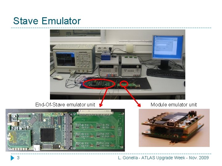
Stave Emulator End-Of-Stave emulator unit 3 Module emulator unit L. Gonella - ATLAS Upgrade Week - Nov. 2009

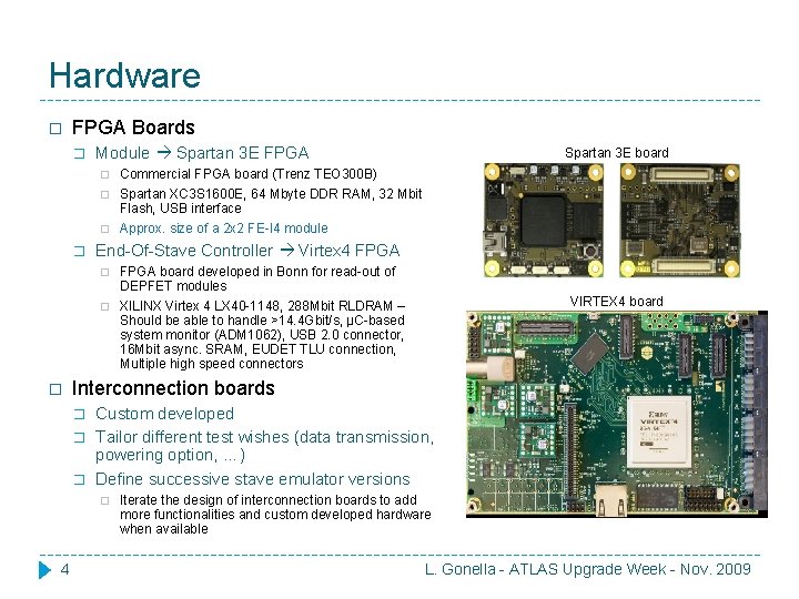
Hardware � FPGA Boards � Module Spartan 3 E FPGA Spartan 3 E board Commercial FPGA board (Trenz TEO 300 B) � Spartan XC 3 S 1600 E, 64 Mbyte DDR RAM, 32 Mbit Flash, USB interface � Approx. size of a 2 x 2 FE-I 4 module � � End-Of-Stave Controller Virtex 4 FPGA board developed in Bonn for read-out of DEPFET modules � XILINX Virtex 4 LX 40 -1148, 288 Mbit RLDRAM – Should be able to handle >14. 4 Gbit/s, µC-based system monitor (ADM 1062), USB 2. 0 connector, 16 Mbit async. SRAM, EUDET TLU connection, Multiple high speed connectors � � Interconnection boards � � � Custom developed Tailor different test wishes (data transmission, powering option, …) Define successive stave emulator versions � 4 VIRTEX 4 board Iterate the design of interconnection boards to add more functionalities and custom developed hardware when available L. Gonella - ATLAS Upgrade Week - Nov. 2009

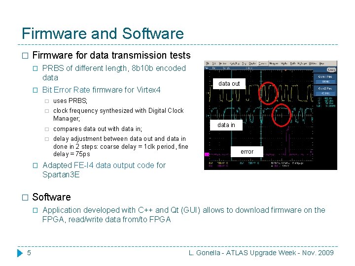
Firmware and Software � Firmware for data transmission tests � PRBS of different length, 8 b 10 b encoded data � Bit Error Rate firmware for Virtex 4 � � � uses PRBS; � clock frequency synthesized with Digital Clock Manager; � compares data out with data in; � delay adjustment between data out and data in done in 2 steps: coarse delay = 1 clk period, fine delay = 75 ps data in error Adapted FE-I 4 data output code for Spartan 3 E Software � 5 data out Application developed with C++ and Qt (GUI) allows to download firmware on the FPGA, read/write data from/to FPGA L. Gonella - ATLAS Upgrade Week - Nov. 2009

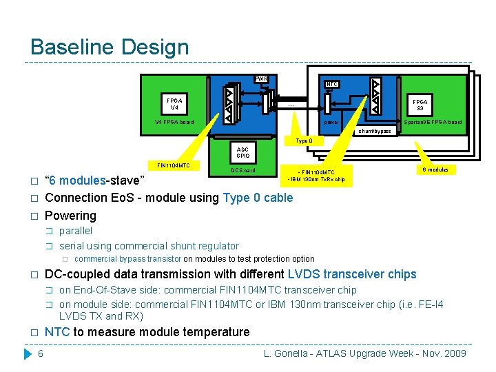
Baseline Design PWR … FPGA V 4 NTC FPGA S 3 … V 4 FPGA board Spartan 3 E FPGA board power shunt/bypass Type 0 ADC GPIO FIN 1104 MTC � � commercial bypass transistor on modules to test protection option DC-coupled data transmission with different LVDS transceiver chips � � 6 6 modules parallel serial using commercial shunt regulator � � • FIN 1104 MTC • IBM 130 nm Tx. Rx chip “ 6 modules-stave” Connection Eo. S - module using Type 0 cable Powering � � DCS card on End-Of-Stave side: commercial FIN 1104 MTC transceiver chip on module side: commercial FIN 1104 MTC or IBM 130 nm transceiver chip (i. e. FE-I 4 LVDS TX and RX) NTC to measure module temperature L. Gonella - ATLAS Upgrade Week - Nov. 2009

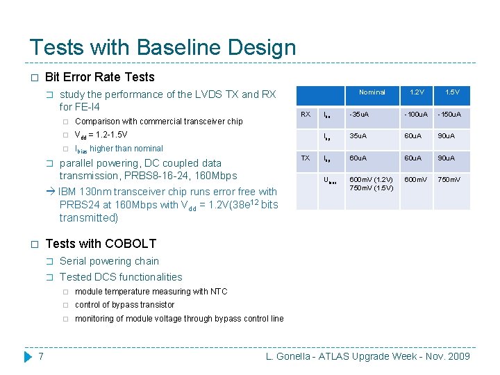
Tests with Baseline Design � Bit Error Rate Tests � � study the performance of the LVDS TX and RX for FE-I 4 � Comparison with commercial transceiver chip � Vdd = 1. 2 -1. 5 V � Ibias higher than nominal Nominal RX TX parallel powering, DC coupled data transmission, PRBS 8 -16 -24, 160 Mbps IBM 130 nm transceiver chip runs error free with PRBS 24 at 160 Mbps with Vdd = 1. 2 V(38 e 12 bits 1. 2 V 1. 5 V Ibn -35 u. A -100 u. A -150 u. A Ibp 35 u. A 60 u. A 90 u. A Ibp 60 u. A 90 u. A Ubias 600 m. V (1. 2 V) 750 m. V (1. 5 V) 600 m. V 750 m. V transmitted) � 7 Tests with COBOLT � Serial powering chain � Tested DCS functionalities � module temperature measuring with NTC � control of bypass transistor � monitoring of module voltage through bypass control line L. Gonella - ATLAS Upgrade Week - Nov. 2009

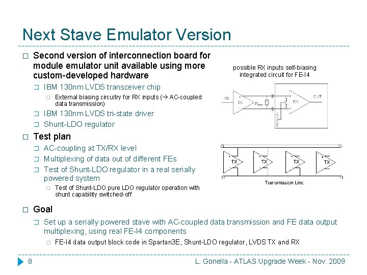
Next Stave Emulator Version � Second version of interconnection board for module emulator unit available using more custom-developed hardware � IBM 130 nm LVDS transceiver chip � � � IBM 130 nm LVDS tri-state driver Shunt-LDO regulator AC-coupling at TX/RX level Multiplexing of data out of different FEs Test of Shunt-LDO regulator in a real serially powered system � Test of Shunt-LDO pure LDO regulator operation with shunt capability switched-off Goal � Set up a serially powered stave with AC-coupled data transmission and FE data output multiplexing, using real FE-I 4 components � 8 External biasing circuitry for RX inputs ( AC-coupled data transmission) Test plan � � possible RX inputs self-biasing integrated circuit for FE-I 4 data output block code in Spartan 3 E, Shunt-LDO regulator, LVDS TX and RX L. Gonella - ATLAS Upgrade Week - Nov. 2009

Towards s. LHC Stave Prototyping � Before FE-I 4 � � Implement more FE-I 4 code in the Spartan 3 E � next step: command decoder � useful also for debugging/developing FE-I 4 test systems Start working on End-Of-Stave controller � � Keep qualifying custom developed hardware in a pixel stave environment � � Module Protection Chip for serial powering, cables/flex and connectors, … After FE-I 4 � 9 Try to implement GBT functionalities (? ) The End-Of-Stave emulator unit can be used as lab DAQ system for real FE-I 4 modules/stave L. Gonella - ATLAS Upgrade Week - Nov. 2009

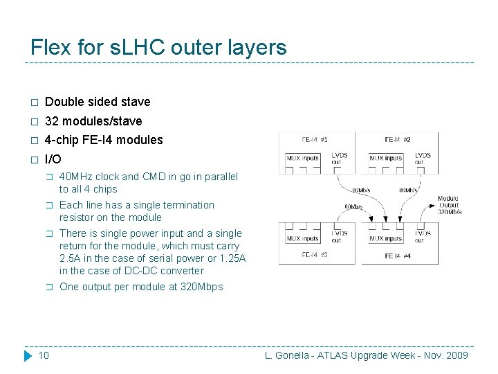
Flex for s. LHC outer layers � Double sided stave � 32 modules/stave � 4 -chip FE-I 4 modules � I/O � 40 MHz clock and CMD in go in parallel to all 4 chips � Each line has a single termination resistor on the module � There is single power input and a single return for the module, which must carry 2. 5 A in the case of serial power or 1. 25 A in the case of DC-DC converter � One output per module at 320 Mbps 10 L. Gonella - ATLAS Upgrade Week - Nov. 2009

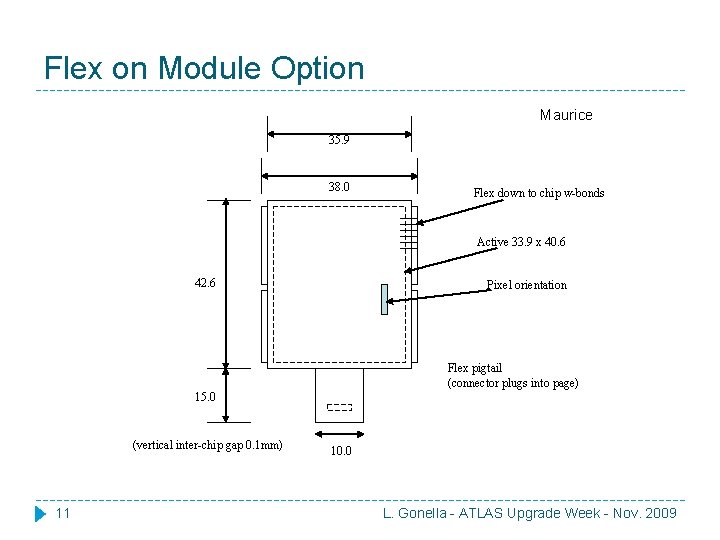
Flex on Module Option Maurice 35. 9 38. 0 Flex down to chip w-bonds Active 33. 9 x 40. 6 42. 6 Pixel orientation Flex pigtail (connector plugs into page) 15. 0 (vertical inter-chip gap 0. 1 mm) 11 10. 0 L. Gonella - ATLAS Upgrade Week - Nov. 2009

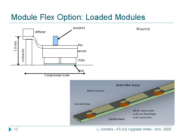
Module Flex Option: Loaded Modules passives Maurice flex connector 1. 0 mm stiffener sensor chips glue Compressed scale 12 L. Gonella - ATLAS Upgrade Week - Nov. 2009

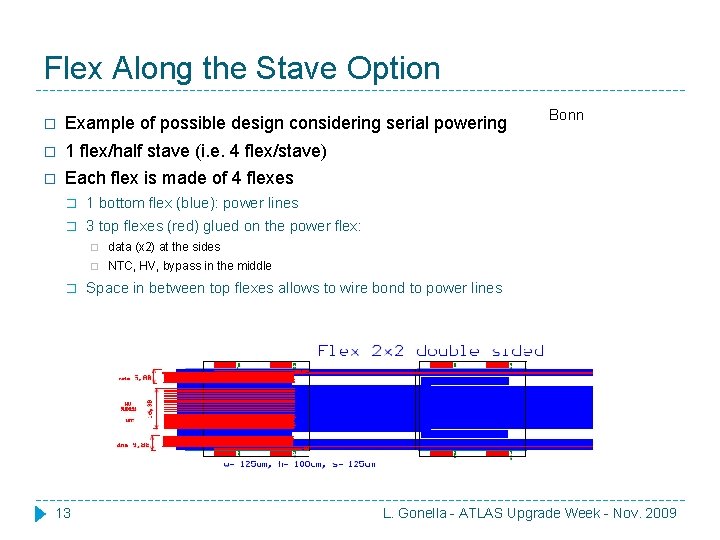
Flex Along the Stave Option � Example of possible design considering serial powering � 1 flex/half stave (i. e. 4 flex/stave) � Each flex is made of 4 flexes � 1 bottom flex (blue): power lines � 3 top flexes (red) glued on the power flex: � 13 � data (x 2) at the sides � NTC, HV, bypass in the middle Bonn Space in between top flexes allows to wire bond to power lines L. Gonella - ATLAS Upgrade Week - Nov. 2009

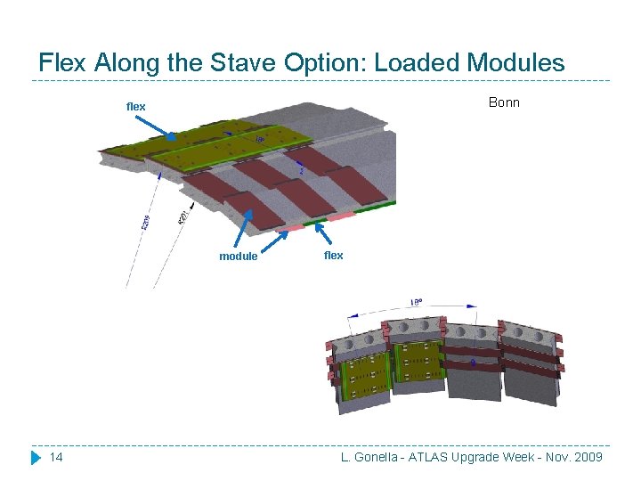
Flex Along the Stave Option: Loaded Modules Bonn flex module 14 flex L. Gonella - ATLAS Upgrade Week - Nov. 2009