Status report of the FATALIC project Laurent Royer
![FATALIC_4 includes: - the analog core ([current conveyor + 3 shapers] FATALIC_3) - 3 FATALIC_4 includes: - the analog core ([current conveyor + 3 shapers] FATALIC_3) - 3](https://slidetodoc.com/presentation_image_h/0ceb0a66f7c9fc921ede24594a8c78fb/image-4.jpg)
- Slides: 17

Status report of the FATALIC project Laurent Royer on behalf of the MICRHAU team 23/02/2021 Laurent. Royer@clermont. in 2 p 3. fr 1

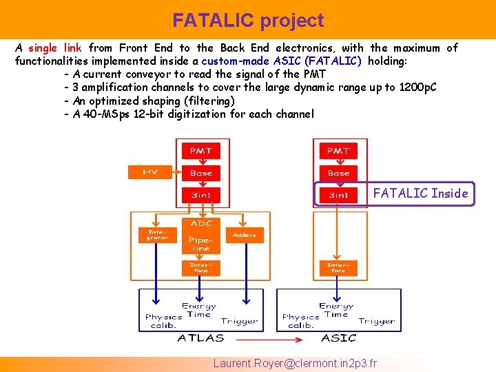
FATALIC project A single link from Front End to the Back End electronics, with the maximum of functionalities implemented inside a custom-made ASIC (FATALIC) holding: - A current conveyor to read the signal of the PMT - 3 amplification channels to cover the large dynamic range up to 1200 p. C - An optimized shaping (filtering) - A 40 -MSps 12 -bit digitization for each channel FATALIC Inside Laurent. Royer@clermont. in 2 p 3. fr

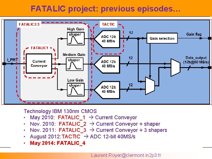
FATALIC project: previous episodes… FATALIC 2 -3 TACTIC FATALIC 1 Technology IBM 130 nm CMOS • May 2010: FATALIC_1 Current Conveyor • Nov. 2010: FATALIC_2 Current Conveyor + shaper • Nov. 2011: FATALIC_3 Current Conveyor + 3 shapers • August 2012: TACTIC ADC 12 -bit 40 MS/s • May 2014: FATALIC_4 Laurent. Royer@clermont. in 2 p 3. fr
![FATALIC4 includes the analog core current conveyor 3 shapers FATALIC3 3 FATALIC_4 includes: - the analog core ([current conveyor + 3 shapers] FATALIC_3) - 3](https://slidetodoc.com/presentation_image_h/0ceb0a66f7c9fc921ede24594a8c78fb/image-4.jpg)
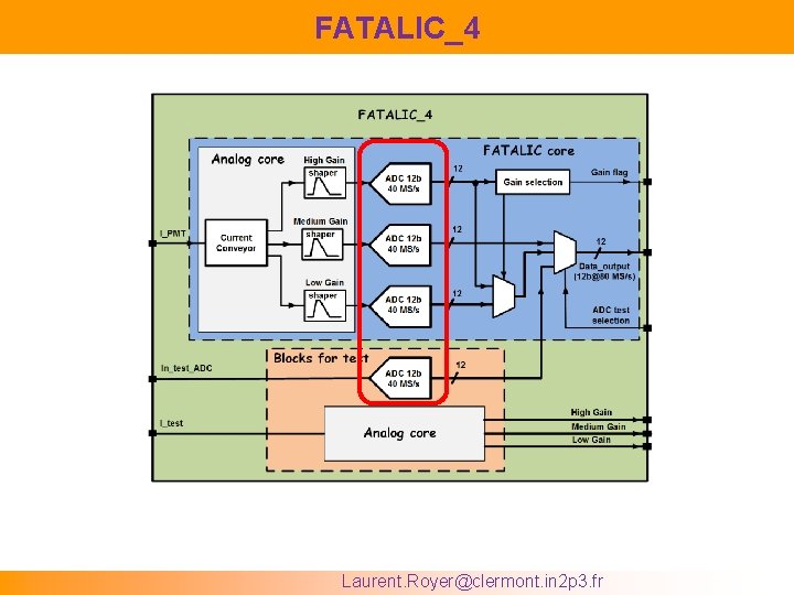
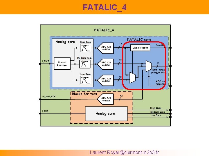
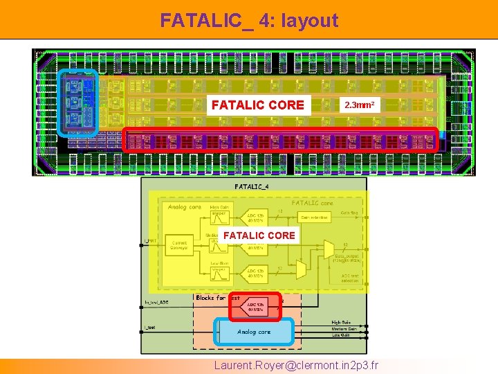
FATALIC_4 includes: - the analog core ([current conveyor + 3 shapers] FATALIC_3) - 3 ADCs (one per gain) TACTIC - A digital data processing - Two independent blocks (analog core and ADC) for test purpose Laurent. Royer@clermont. in 2 p 3. fr

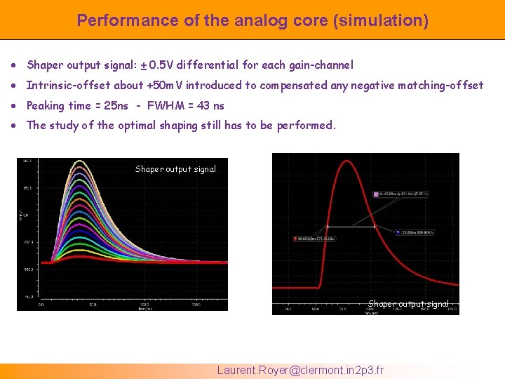
Performance of the analog core (simulation) Shaper output signal: ± 0. 5 V differential for each gain-channel Intrinsic-offset about +50 m. V introduced to compensated any negative matching-offset Peaking time = 25 ns - FWHM = 43 ns The study of the optimal shaping still has to be performed. Shaper output signal Laurent. Royer@clermont. in 2 p 3. fr

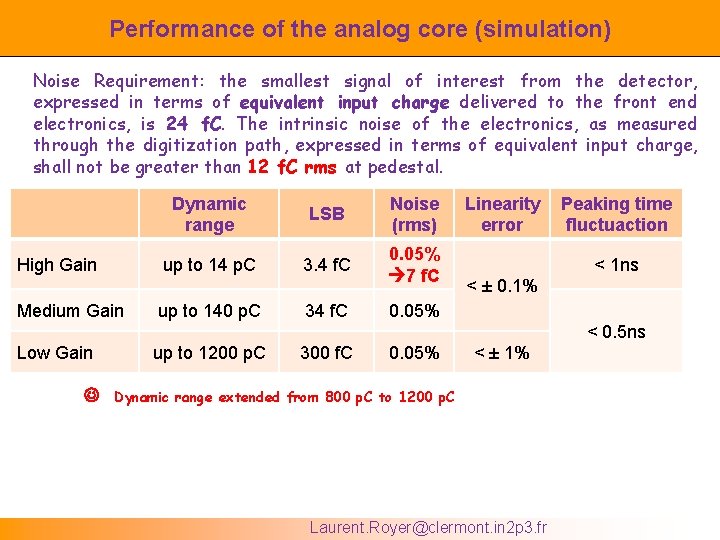
Performance of the analog core (simulation) Noise Requirement: the smallest signal of interest from the detector, expressed in terms of equivalent input charge delivered to the front end electronics, is 24 f. C. The intrinsic noise of the electronics, as measured through the digitization path, expressed in terms of equivalent input charge, shall not be greater than 12 f. C rms at pedestal. High Gain Medium Gain Dynamic range LSB Noise (rms) up to 14 p. C 3. 4 f. C 0. 05% 7 f. C up to 140 p. C 34 f. C Linearity error Peaking time fluctuaction < 1 ns < ± 0. 1% 0. 05% < 0. 5 ns Low Gain up to 1200 p. C 300 f. C 0. 05% < ± 1% Dynamic range extended from 800 p. C to 1200 p. C Shaper output signal Laurent. Royer@clermont. in 2 p 3. fr

FATALIC_4 Laurent. Royer@clermont. in 2 p 3. fr

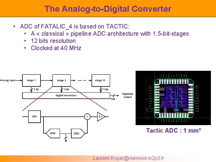
The Analog-to-Digital Converter • ADC of FATALIC_4 is based on TACTIC: • A « classical » pipeline ADC architecture with 1. 5 -bit-stages • 12 bits resolution • Clocked at 40 MHz Tactic ADC : 1 mm² Laurent. Royer@clermont. in 2 p 3. fr

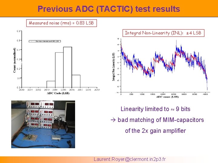
Previous ADC (TACTIC) test results Measured noise (rms) = 0. 83 LSB Integral Non-Linearity (INL): ± 4 LSB Test bench Linearity limited to 9 bits bad matching of MIM-capacitors of the 2 x gain amplifier Laurent. Royer@clermont. in 2 p 3. fr

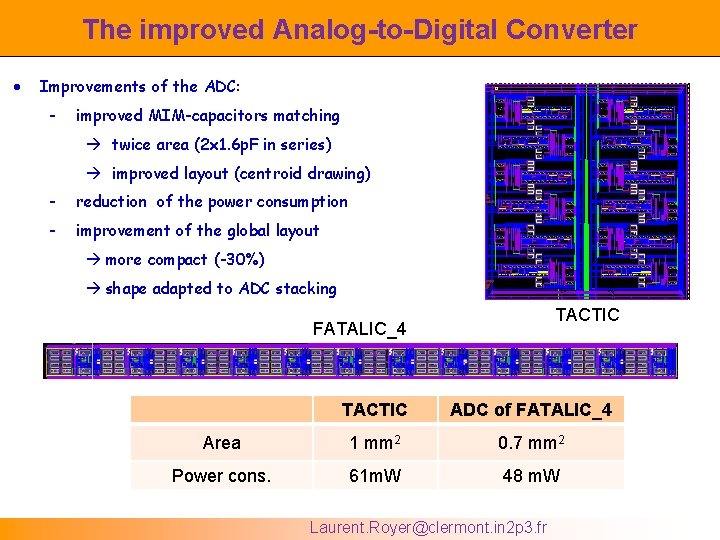
The improved Analog-to-Digital Converter Improvements of the ADC: - improved MIM-capacitors matching twice area (2 x 1. 6 p. F in series) improved layout (centroid drawing) - reduction of the power consumption - improvement of the global layout more compact (-30%) shape adapted to ADC stacking TACTIC FATALIC_4 TACTIC ADC of FATALIC_4 Area 1 mm 2 0. 7 mm 2 Power cons. 61 m. W 48 m. W Laurent. Royer@clermont. in 2 p 3. fr

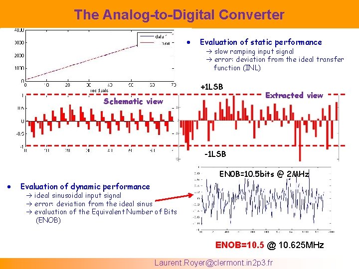
The Analog-to-Digital Converter Evaluation of static performance slow ramping input signal error: deviation from the ideal transfer function (INL) +1 LSB Schematic view Extracted view -1 LSB EN 0 B=10. 5 bits @ 2 MHz Evaluation of dynamic performance ideal sinusoidal input signal error: deviation from the ideal sinus evaluation of the Equivalent Number of Bits (ENOB) ENOB=10. 5 @ 10. 625 MHz Laurent. Royer@clermont. in 2 p 3. fr

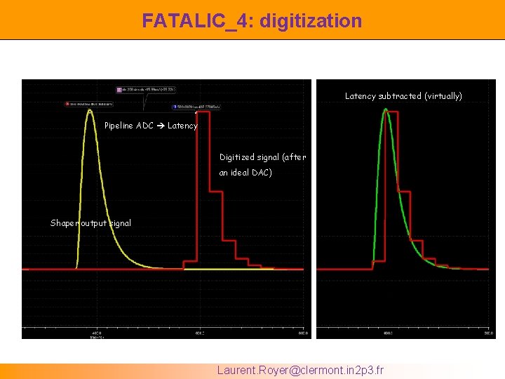
FATALIC_4: digitization Latency subtracted (virtually) Pipeline ADC Latency Digitized signal (after an ideal DAC) Shaper output signal Laurent. Royer@clermont. in 2 p 3. fr

FATALIC_4 Laurent. Royer@clermont. in 2 p 3. fr

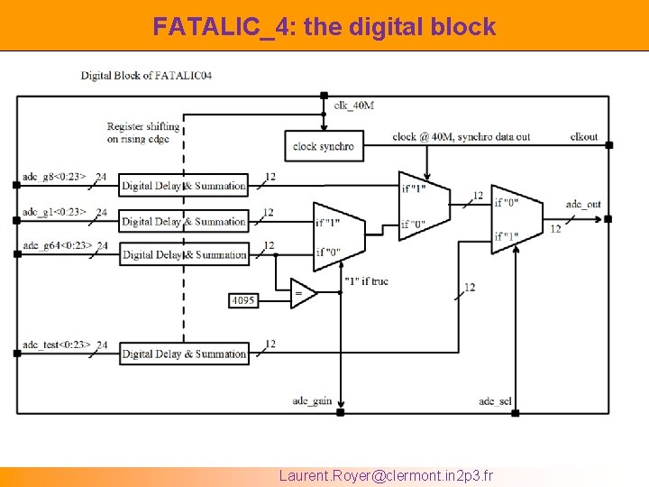
FATALIC_4: the digital block Laurent. Royer@clermont. in 2 p 3. fr

FATALIC_ 4: layout FATALIC CORE 2. 3 mm 2 FATALIC CORE Laurent. Royer@clermont. in 2 p 3. fr

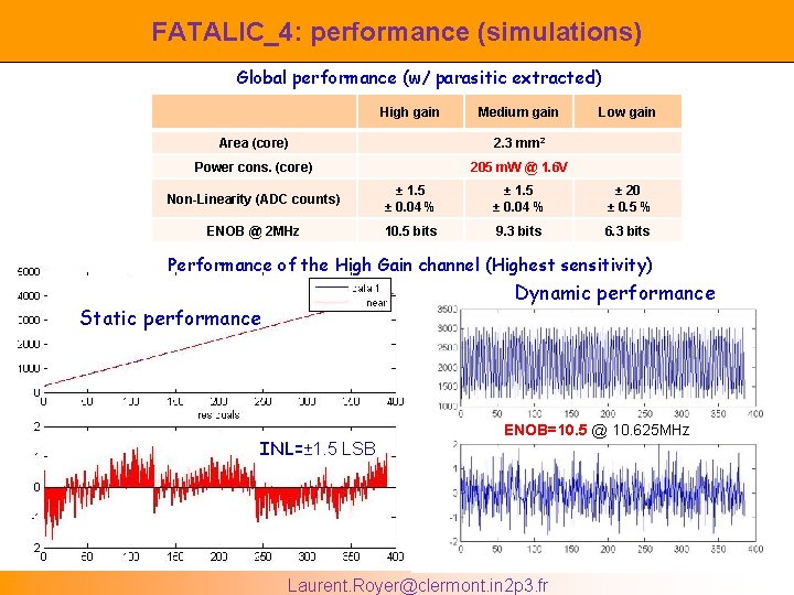
FATALIC_4: performance (simulations) Global performance (w/ parasitic extracted) High gain Medium gain Area (core) 2. 3 mm 2 Power cons. (core) 205 m. W @ 1. 6 V Low gain Non-Linearity (ADC counts) ± 1. 5 ± 0. 04 % ± 20 ± 0. 5 % ENOB @ 2 MHz 10. 5 bits 9. 3 bits 6. 3 bits Performance of the High Gain channel (Highest sensitivity) Dynamic performance Static performance INL=± 1. 5 LSB ENOB=10. 5 @ 10. 625 MHz Laurent. Royer@clermont. in 2 p 3. fr

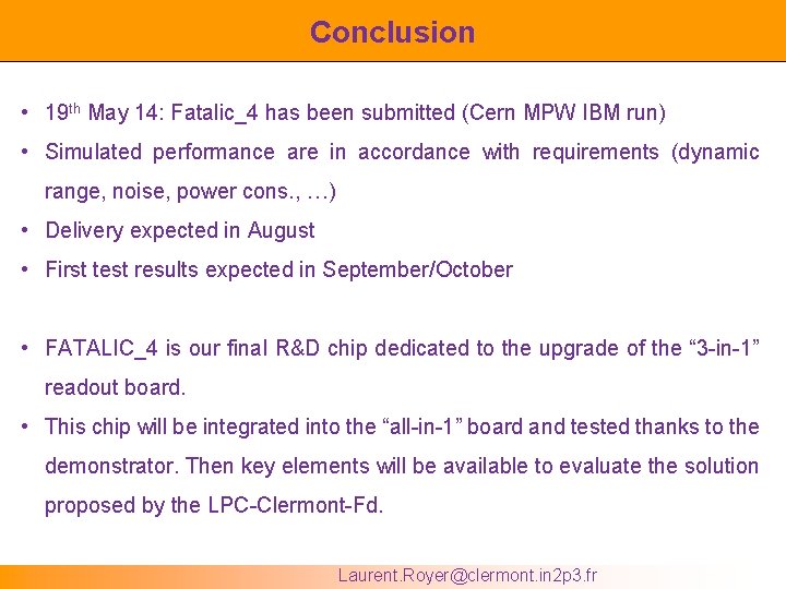
Conclusion • 19 th May 14: Fatalic_4 has been submitted (Cern MPW IBM run) • Simulated performance are in accordance with requirements (dynamic range, noise, power cons. , …) • Delivery expected in August • First test results expected in September/October • FATALIC_4 is our final R&D chip dedicated to the upgrade of the “ 3 -in-1” readout board. • This chip will be integrated into the “all-in-1” board and tested thanks to the demonstrator. Then key elements will be available to evaluate the solution proposed by the LPC-Clermont-Fd. Laurent. Royer@clermont. in 2 p 3. fr