Status of the PANDA MVD Project Intro Physics

- Slides: 32

Status of the PANDA MVD Project • Intro • Physics with the MVD • Design: (INFN-Torino) mechanics and electrics • R&D: soft and hard Kai-Thomas Brinkmann, 2 nd PANDA Russia Workshop, Apr 26, 2010

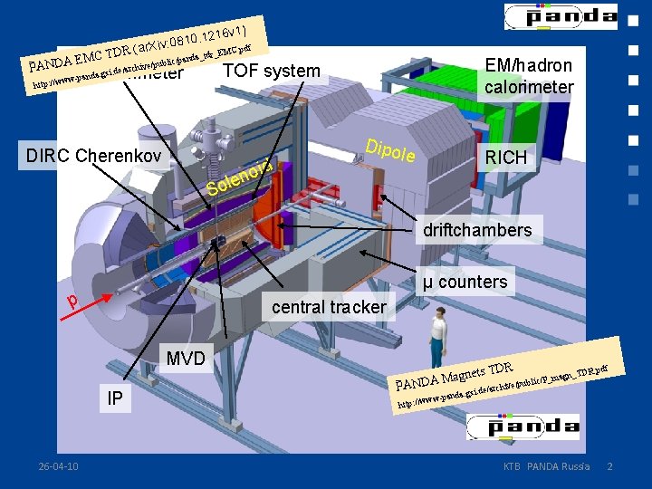
PANDA 216 v 1) 1. 0 1 8 v: 0. pdf R (ar. Xi D r_EMC T C anda_td M E ublic/p hive/p i. de/arc s. g a d n a /www-p http: / EM calorimeter EM/hadron calorimeter TOF system DIRC Cherenkov d noi Dipol e RICH e Sol driftchambers µ counters p central tracker MVD IP 26 -04 -10 R. pdf ets TDR n agn_TD g a m _ M /P c e/publi NDA PA /archiv a. gsi. de w-pand ttp: //ww h KTB PANDA Russia 2

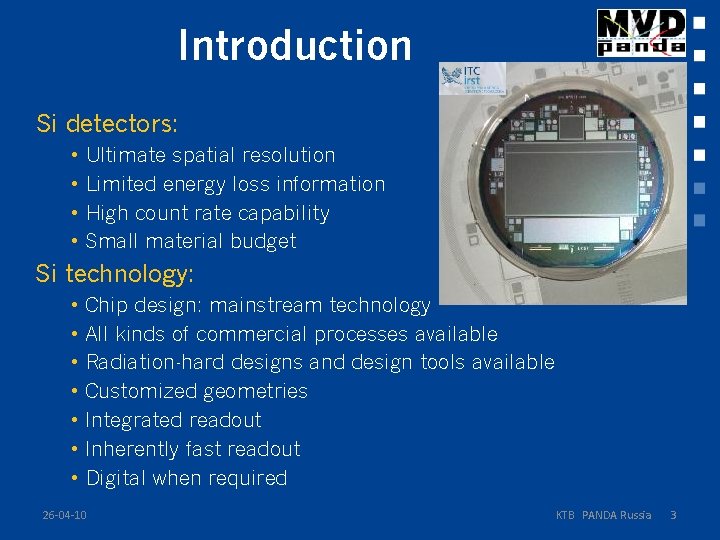
Introduction Si detectors: • • Ultimate spatial resolution Limited energy loss information High count rate capability Small material budget Si technology: • • Chip design: mainstream technology All kinds of commercial processes available Radiation-hard designs and design tools available Customized geometries Integrated readout Inherently fast readout Digital when required 26 -04 -10 KTB PANDA Russia 3

The PANDA Micro-Vertex Detector Design adopts state-of-the-art silicon sensor techniques Focus on PANDA specific issues: • • • High and asynchronous interaction rate Strongly asymmetric angular distributions Versatile experimental requirements D meson ID Minimum mass budget Solutions: • • • Heterogeneous design (pixel and strip sensors) Very compact design Limited number of space points / layers (default 4) Novel readout electronics (non-triggered readout) Tracklets real-time (fast on-line processing) 26 -04 -10 KTB PANDA Russia 4

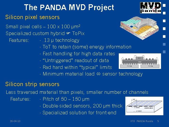
The PANDA MVD Project Silicon pixel sensors Small pixel cells – 100 x 100 µm 2 Specialized custom hybrid To. Pix Features: -. 13 µ technology - To. T to retain (some) energy information - Fast handling for high data rates - “Untriggered” readout of data - Rad hard within “typical” limits - Minimum material load sensor technology Silicon strip sensors Less traversed material than pixels, smaller number of channels Features: - Pitch of 50 – 150 µm - Double-sided sensors, 200 µm thick - Specialized solution for front-end 26 -04 -10 KTB PANDA Russia 5

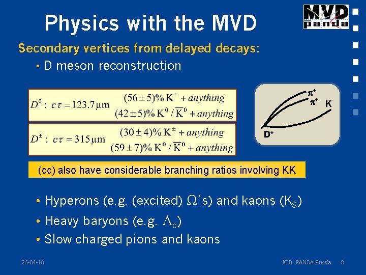
Physics with the MVD Secondary vertices from delayed decays: • D meson reconstruction + + KD+ (cc) also have considerable branching ratios involving KK • Hyperons (e. g. (excited) Ω´s) and kaons (KS) • Heavy baryons (e. g. Λc) • Slow charged pions and kaons 26 -04 -10 KTB PANDA Russia 8

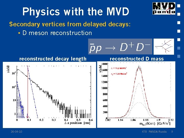
Physics with the MVD Secondary vertices from delayed decays: • D meson reconstruction reconstructed decay length 26 -04 -10 reconstructed D mass KTB PANDA Russia 9

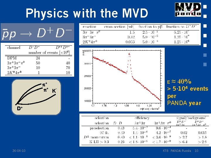
Physics with the MVD + + KD+ 26 -04 -10 ε ≈ 40% > 5∙ 10 4 events per PANDA year KTB PANDA Russia 10

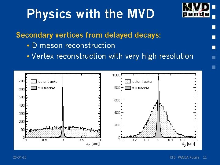
Physics with the MVD Secondary vertices from delayed decays: • D meson reconstruction • Vertex reconstruction with very high resolution 26 -04 -10 KTB PANDA Russia 11

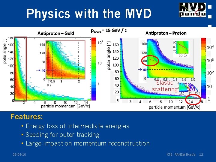
Physics with the MVD Secondary vertices from delayed decays: • D meson reconstruction • vertex reconstruction with very high resolution Elastic scattering Features: • Energy loss at intermediate energies • Seeding for outer tracking • Large impact on momentum reconstruction 26 -04 -10 KTB PANDA Russia 12

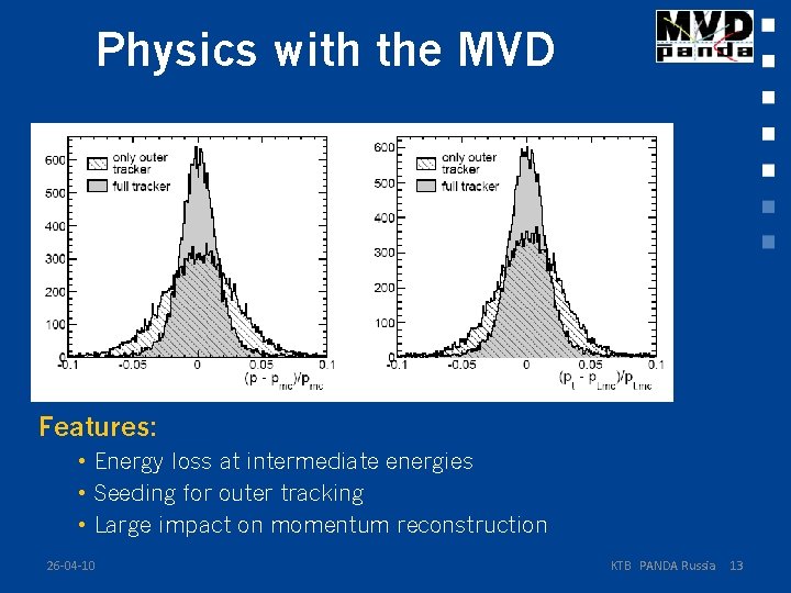
Physics with the MVD Secondary vertices from delayed decays: • D meson reconstruction • vertex reconstruction with very high resolution Features: • Energy loss at intermediate energies • Seeding for outer tracking • Large impact on momentum reconstruction 26 -04 -10 KTB PANDA Russia 13

Design 26 -04 -10 KTB PANDA Russia 14

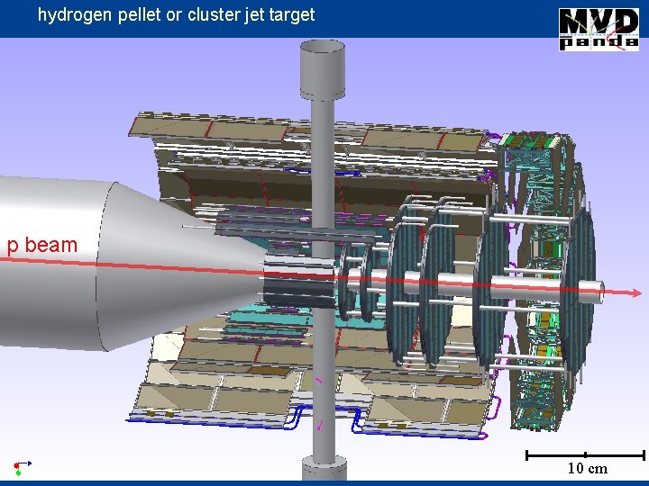
hydrogen pellet or cluster jet target p beam 06 -11 -09 KTB Uppsala 15 10 cm

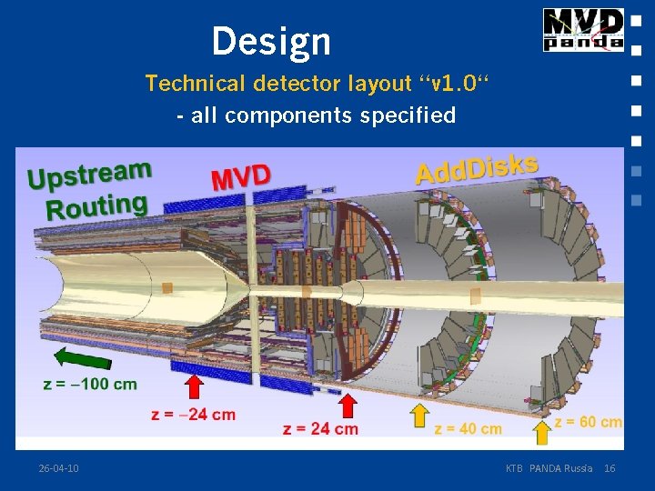
Design Technical detector layout “v 1. 0“ - all components specified 26 -04 -10 KTB PANDA Russia 16

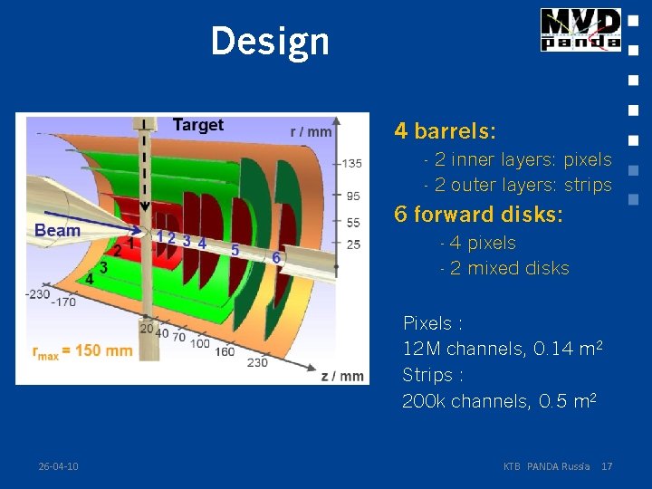
Design 4 barrels: - 2 inner layers: pixels - 2 outer layers: strips 6 forward disks: - 4 pixels - 2 mixed disks Pixels : 12 M channels, 0. 14 m 2 Strips : 200 k channels, 0. 5 m 2 26 -04 -10 KTB PANDA Russia 17

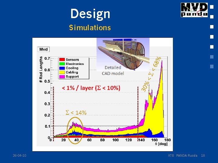
Design Simulations 26 -04 -10 KTB PANDA Russia 18

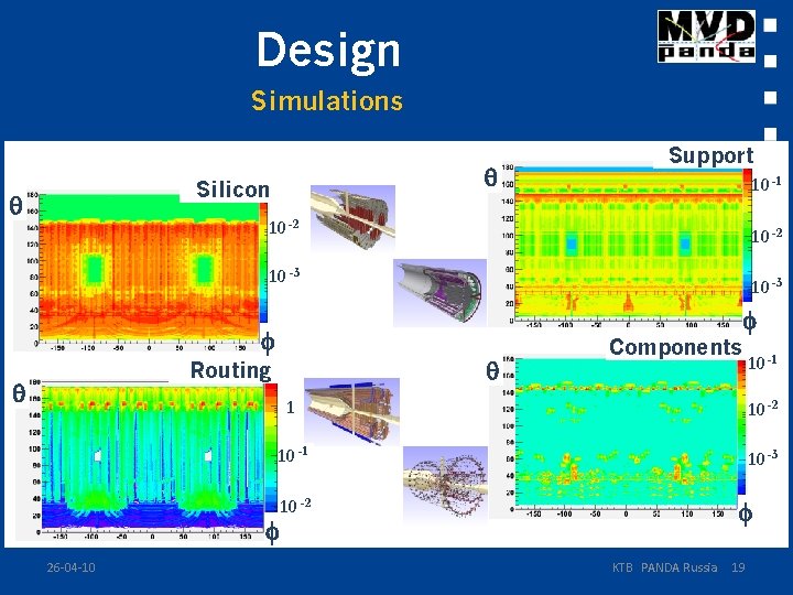
Design Simulations Silicon Support 10 -1 10 -2 10 -3 Routing Components 10 -1 1 10 -2 10 -1 10 -3 26 -04 -10 10 -3 10 -2 KTB PANDA Russia 19

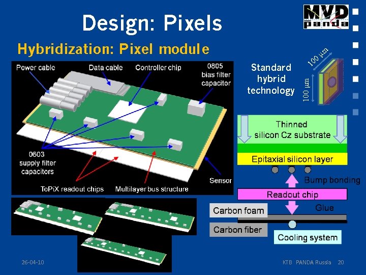
Design: Pixels Standard hybrid technology 26 -04 -10 μm 0 10 100 μm Hybridization: Pixel module KTB PANDA Russia 20

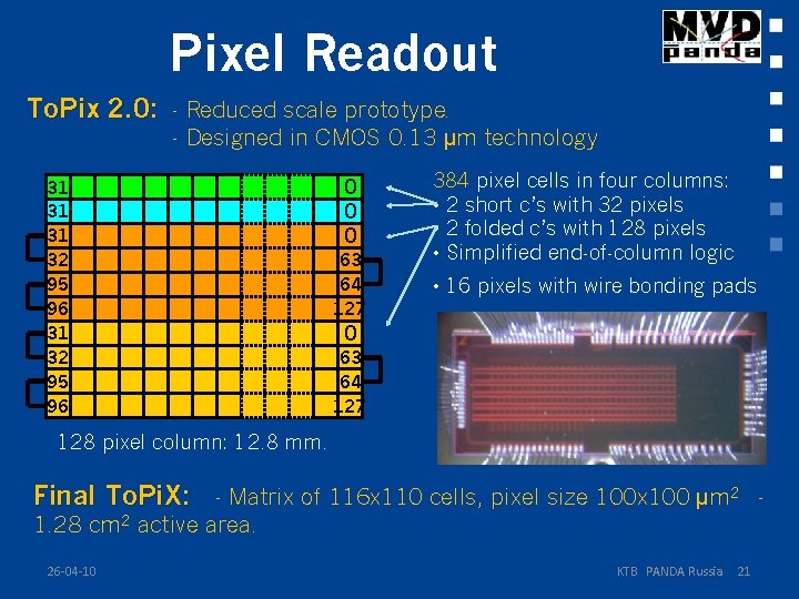
Pixel Readout To. Pix 2. 0: - Reduced scale prototype. - Designed in CMOS 0. 13 μm technology 31 31 31 32 95 96 0 0 0 63 64 127 384 pixel cells in four columns: • 2 short c’s with 32 pixels • 2 folded c’s with 128 pixels • Simplified end-of-column logic • 16 pixels with wire bonding pads 0 63 64 127 128 pixel column: 12. 8 mm. Final To. Pi. X: - Matrix of 116 x 110 cells, pixel size 100 x 100 μm 2 1. 28 cm 2 active area. 26 -04 -10 KTB PANDA Russia 21

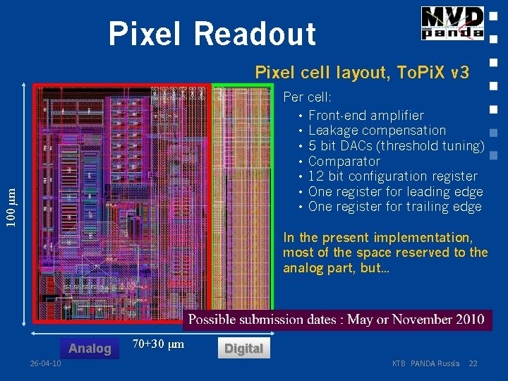
Pixel Readout Pixel cell layout, To. Pi. X v 3 100 µm Per • • cell: Front-end amplifier Leakage compensation 5 bit DACs (threshold tuning) Comparator 12 bit configuration register One register for leading edge One register for trailing edge In the present implementation, most of the space reserved to the analog part, but… Analog 26 -04 -10 70+30 μm Digital KTB PANDA Russia 22

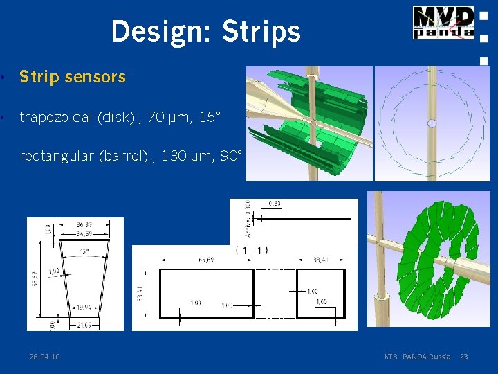
Design: Strips • Strip sensors • trapezoidal (disk) , 70 µm, 15° rectangular (barrel) , 130 µm, 90° 26 -04 -10 KTB PANDA Russia 23

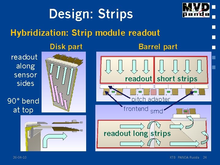
Design: Strips Hybridization: Strip module readout Disk part readout along sensor sides 90° bend at top Barrel part readout short strips pitch adapter frontend smd readout long strips 26 -04 -10 KTB PANDA Russia 24

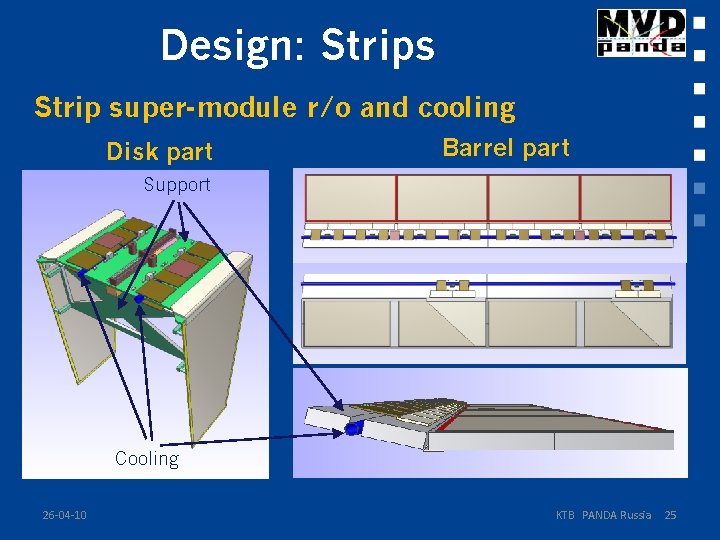
Design: Strips Strip super-module r/o and cooling Disk part Barrel part Support Cooling 26 -04 -10 KTB PANDA Russia 25

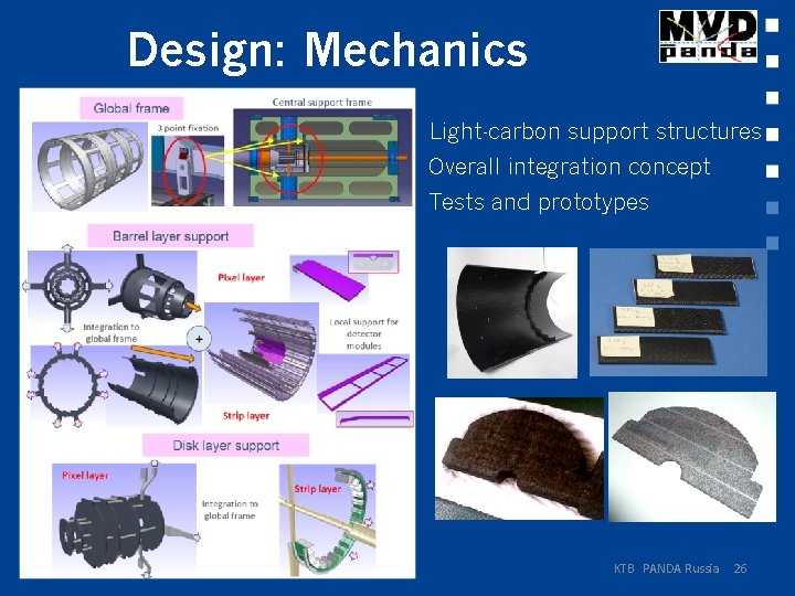
Design: Mechanics Light-carbon support structures Overall integration concept Tests and prototypes 26 -04 -10 KTB PANDA Russia 26

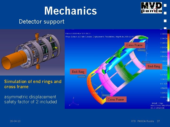
Mechanics Detector support Cross Frame End-Ring Simulation of end rings and cross frame asymmetric displacement safety factor of 2 included 26 -04 -10 Cross Frame KTB PANDA Russia 27

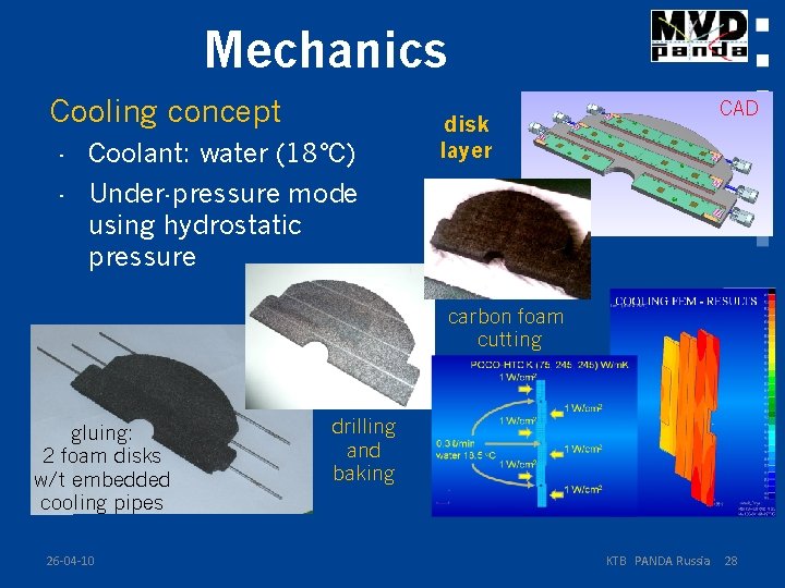
Mechanics Cooling concept - Coolant: water (18°C) CAD disk layer - Under-pressure mode using hydrostatic pressure carbon foam cutting gluing: 2 foam disks w/t embedded cooling pipes 26 -04 -10 drilling and baking KTB PANDA Russia 28

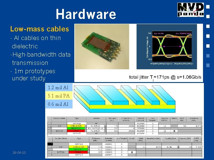
Hardware Low-mass cables - Al cables on thin dielectric -High-bandwidth data transmission - 1 m prototypes under study 1. 2 mil Al 5. 1 mil PA 0. 6 mil Al 26 -04 -10 KTB PANDA Russia 29

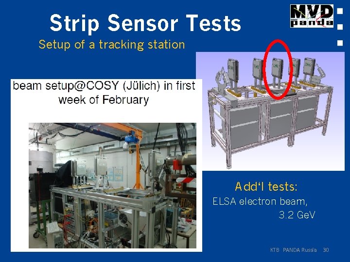
Strip Sensor Tests Setup of a tracking station Add‘l tests: ELSA electron beam, 3. 2 Ge. V 26 -04 -10 KTB PANDA Russia 30

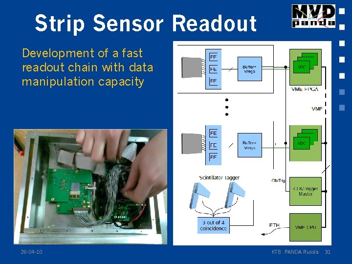
Strip Sensor Readout Development of a fast readout chain with data manipulation capacity 26 -04 -10 KTB PANDA Russia 31

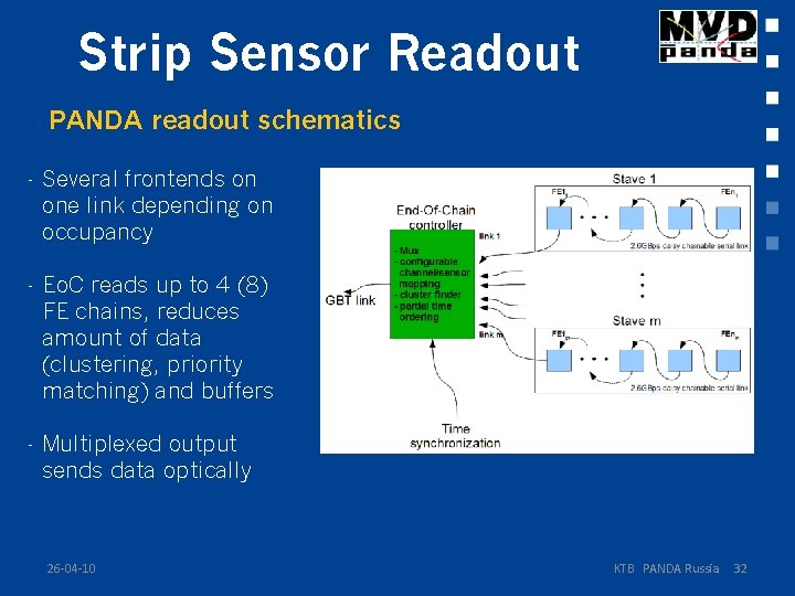
Strip Sensor Readout PANDA readout schematics - Several frontends on one link depending on occupancy - Eo. C reads up to 4 (8) FE chains, reduces amount of data (clustering, priority matching) and buffers - Multiplexed output sends data optically 26 -04 -10 KTB PANDA Russia 32

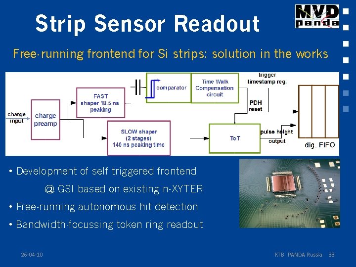
Strip Sensor Readout Free-running frontend for Si strips: solution in the works • Development of self triggered frontend @ GSI based on existing n-XYTER • Free-running autonomous hit detection • Bandwidth-focussing token ring readout 26 -04 -10 KTB PANDA Russia 33

Summary The MVD concept: • needs continued R&D. • has to undergo add‘l iterations with simulation. • has reached a technical level. • meets the design specifications. R&D as well as the realization of the microvertex detector needs expert manpower. 26 -04 -10 KTB PANDA Russia 34