Status of the GBTXLTB Link Test Board Tullio

Status of the GBTX-LTB (Link Test Board) Tullio Grassi 15 March 2013
Overall status The GBTX-LTB firmware is now in a much better situation (many thanks to Sophie and David). Still a lot of work needed for the integration with the tester and the sequence to be executed on the tester. Files related to this presentations on: https: //espace. cern. ch/GBT-Project/GBTX/design/Tests/ GBTX-LTB GBTX_LTB_v 3_6 2
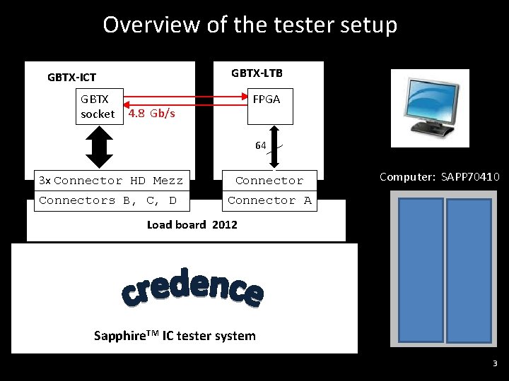
Overview of the tester setup GBTX-LTB GBTX-ICT GBTX socket FPGA 4. 8 Gb/s 64 3 x Connector HD Mezz Connectors B, C, D Connector A Computer: SAPP 70410 Load board 2012 Sapphire. TM IC tester system 3
To-do list from the previous meeting 1. Debug the GBT problem DONE, see next slides 2. Remove the Flip Flop for the Tester loopback DONE 3. Use the 31 st bit sent to the Tester as a logic-OR of all the Locked, Ready bits from PLLs and CDR DONE (DV used as a CDR_ready bit ) 4. Install Xilinx Chipscope on the Tester computer DONE (no more need for a separate computer) 5. Use the Tester Ubits to set the operating mode of the FPGA STILL MISTERIES (Cannot control them, ~5 V seen on LTB !? NB: LTB FPGA is not 5 V-tolerant) 6. Study if it is possible to obtain from the FPGA compiler a full model of the FPGA that could be simulated “stand-alone”. This would allow to build a full model for generating the test vectors. IN PROGRESS 7. Implement the idle-header / data-header functionality in the GBT-FPGA code 8. Make sure all the clocks have phases well defined (and known) phases. 4
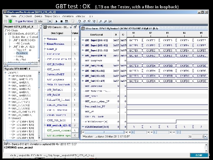
GBT test : OK (LTB on the Tester, with a fiber in loopback) 5
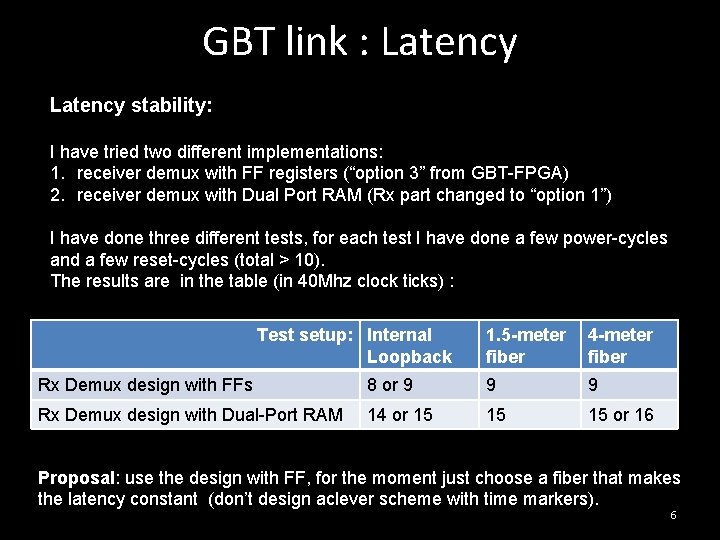
GBT link : Latency stability: I have tried two different implementations: 1. receiver demux with FF registers (“option 3” from GBT-FPGA) 2. receiver demux with Dual Port RAM (Rx part changed to “option 1”) I have done three different tests, for each test I have done a few power-cycles and a few reset-cycles (total > 10). The results are in the table (in 40 Mhz clock ticks) : Test setup: Internal Loopback 1. 5 -meter fiber 4 -meter fiber Rx Demux design with FFs 8 or 9 9 9 Rx Demux design with Dual-Port RAM 14 or 15 15 15 or 16 Proposal: use the design with FF, for the moment just choose a fiber that makes the latency constant (don’t design aclever scheme with time markers). 6
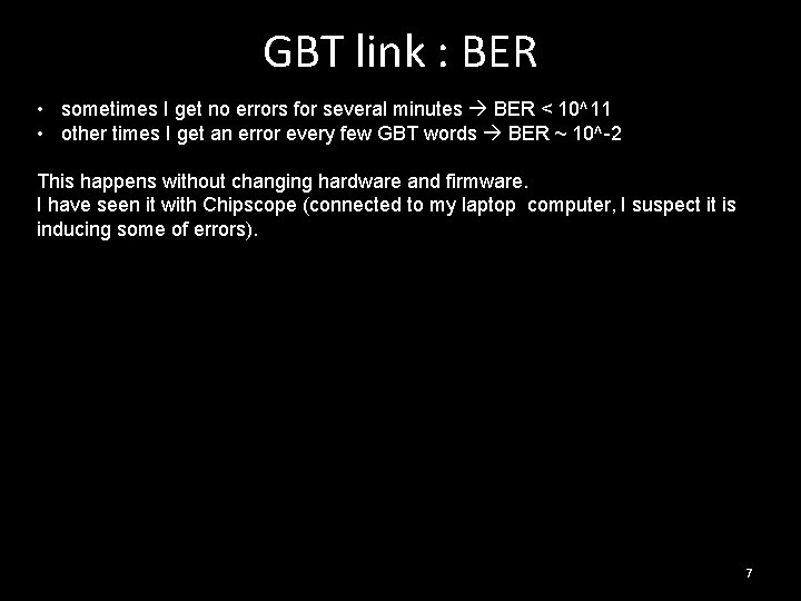
GBT link : BER • sometimes I get no errors for several minutes BER < 10^11 • other times I get an error every few GBT words BER ~ 10^-2 This happens without changing hardware and firmware. I have seen it with Chipscope (connected to my laptop computer, I suspect it is inducing some of errors). 7
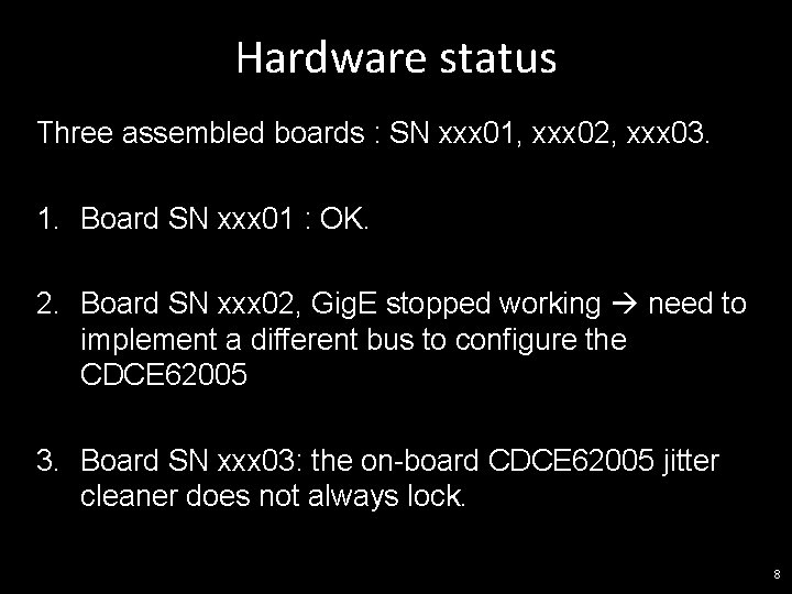
Hardware status Three assembled boards : SN xxx 01, xxx 02, xxx 03. 1. Board SN xxx 01 : OK. 2. Board SN xxx 02, Gig. E stopped working need to implement a different bus to configure the CDCE 62005 3. Board SN xxx 03: the on-board CDCE 62005 jitter cleaner does not always lock. 8
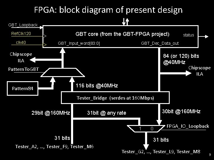
FPGA: block diagram of present design GBT_Loopback GBT core (from the GBT-FPGA project) Ref. Clk 120 clk 40 GBT_Input_word[83: 0] status GBT_Dec_Data_out Chipscope ILA 84 (or 120) bits @40 MHz Chipscope ILA Pattern. To. GBT 116 bits @40 MHz Pattern 84 Tester_Bridge (serdes at 160 Mbps) 29 bit @160 MHz 30 bit @160 MHz 31 bit @ any rate 1 31 bits Tester_A 2, …, Tester_F 9, Tester_M 6 0 FPGA_IO_Loopback 31 bits Tester_G 2, …, Tester_L 9, Tester_M 8 9
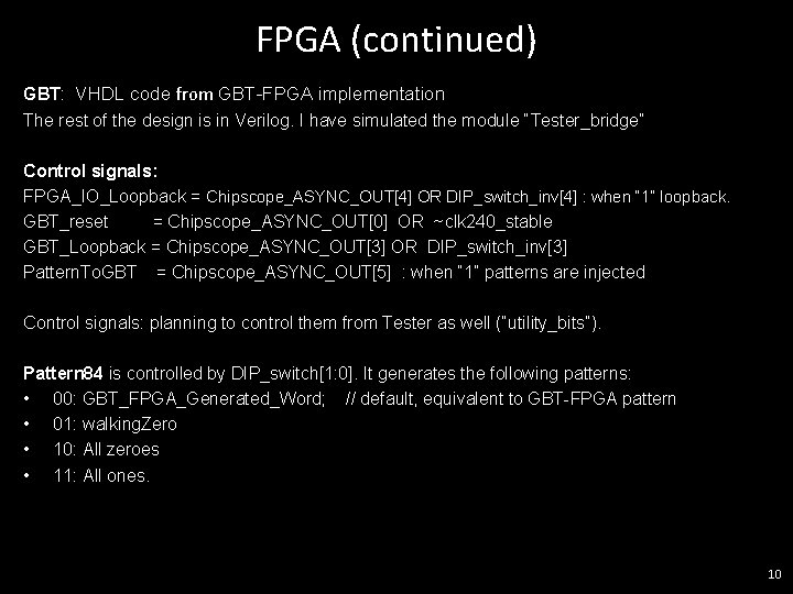
FPGA (continued) GBT: VHDL code from GBT-FPGA implementation The rest of the design is in Verilog. I have simulated the module “Tester_bridge” Control signals: FPGA_IO_Loopback = Chipscope_ASYNC_OUT[4] OR DIP_switch_inv[4] : when “ 1” loopback. GBT_reset = Chipscope_ASYNC_OUT[0] OR ~clk 240_stable GBT_Loopback = Chipscope_ASYNC_OUT[3] OR DIP_switch_inv[3] Pattern. To. GBT = Chipscope_ASYNC_OUT[5] : when “ 1” patterns are injected Control signals: planning to control them from Tester as well (“utility_bits”). Pattern 84 is controlled by DIP_switch[1: 0]. It generates the following patterns: • 00: GBT_FPGA_Generated_Word; // default, equivalent to GBT-FPGA pattern • 01: walking. Zero • 10: All zeroes • 11: All ones. 10
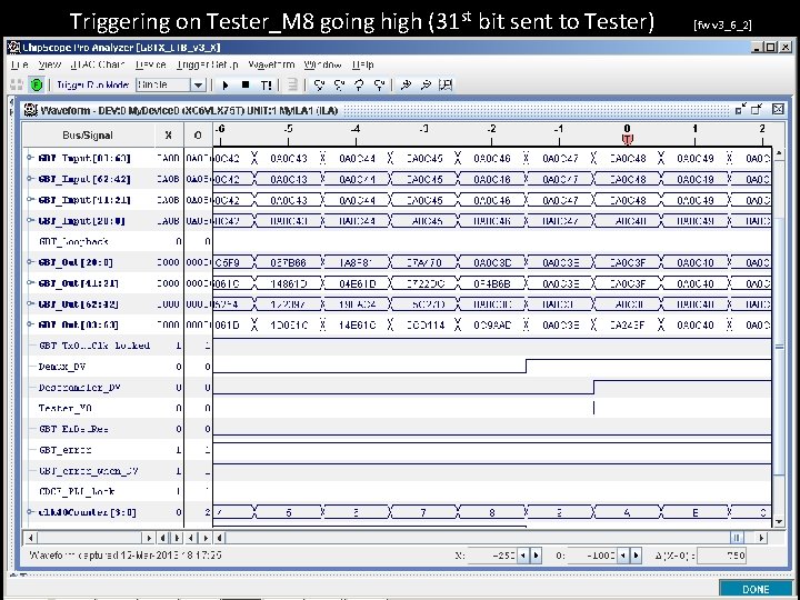
Triggering on Tester_M 8 going high (31 st bit sent to Tester) [fw v 3_6_2] 11
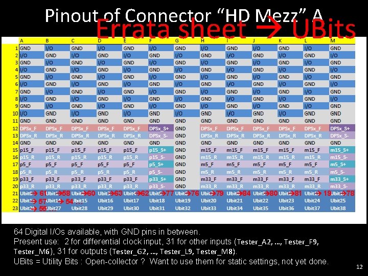
Pinout of Connector “HD Mezz” A Errata sheet UBits 61 58 60 57 54 … 55 … 63 62 77 76 79 84 80 81 19 64 Digital I/Os available, with GND pins in between. Present use: 2 for differential clock input, 31 for other inputs (Tester_A 2, …, Tester_F 9, Tester_M 6), 31 for outputs (Tester_G 2, …, Tester_L 9, Tester_M 8). UBits = Utility Bits : Open-collector ? Want to use them for static settings, not yet done. 78 12
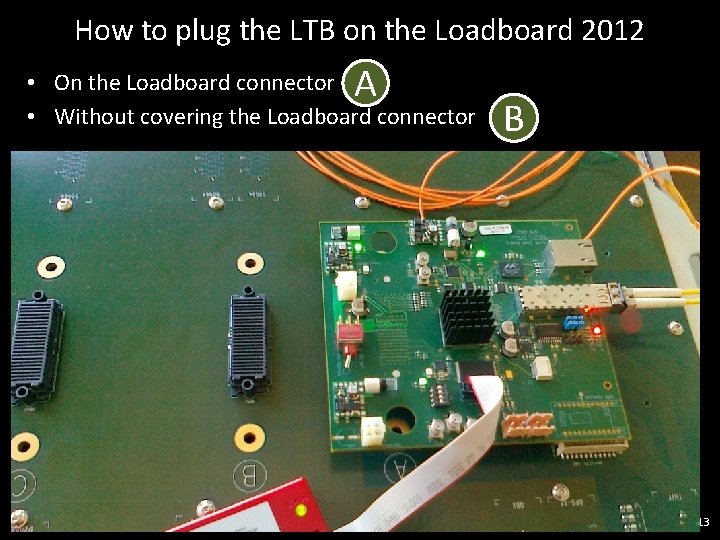
How to plug the LTB on the Loadboard 2012 A • On the Loadboard connector • Without covering the Loadboard connector B 13
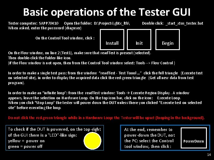
Basic operations of the Tester GUI Tester computer: SAPP 70410 Open the folder: D: Projectsgbtx_ltb When asked, enter the password (diaguser) On the Control Tool window, click : Install Double click: _start_xtos_tester. bat Init Begin On the Flow window, on line 2 (Test 1), make sure that read. Test is present (selected). Then double-click the folder-like icon. (if the Flow window is not open, then from the Control Tool window select: Tools --> Flow Control ) In order to make a single test pass: from the window “read. Test - Test Toool …” click the full triangle (Execute test on selected site), in order to display the acquired data click the red-green triangle (Get all new data from test program). In order to make an “infinite loop”: from the read. Test window: Tools → Execute Region Display. A window appears, leave the selection on Hardware Loop. On the top icon bar, click on the icon: Execute Loop. When you click “Stop Loop” the tester will power down the DUT unless there you clicked “Execute test on selected site” before executing the loop. Do not click the red-green triangle while in a Hardware Loop: the Tester will be upset (looping in the background). To check if the DUT is powered, on the top-right of the GUI there is a "LED"-like sign: yellow = power on green = power off At the end, remember to power-down the DUT, not the PC: select the Control tool window, then click : Power. Down 14
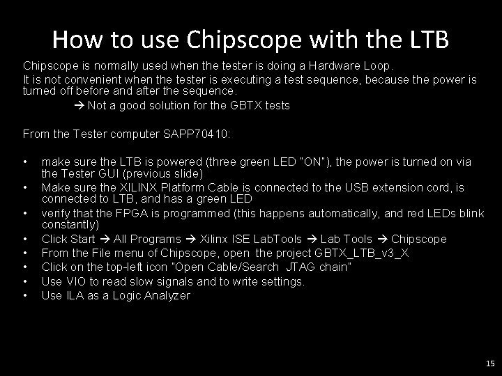
How to use Chipscope with the LTB Chipscope is normally used when the tester is doing a Hardware Loop. It is not convenient when the tester is executing a test sequence, because the power is turned off before and after the sequence. Not a good solution for the GBTX tests From the Tester computer SAPP 70410: • • make sure the LTB is powered (three green LED “ON”), the power is turned on via the Tester GUI (previous slide) Make sure the XILINX Platform Cable is connected to the USB extension cord, is connected to LTB, and has a green LED verify that the FPGA is programmed (this happens automatically, and red LEDs blink constantly) Click Start All Programs Xilinx ISE Lab. Tools Lab Tools Chipscope From the File menu of Chipscope, open the project GBTX_LTB_v 3_X Click on the top-left icon “Open Cable/Search JTAG chain” Use VIO to read slow signals and to write settings. Use ILA as a Logic Analyzer 15

Back-up slides 16
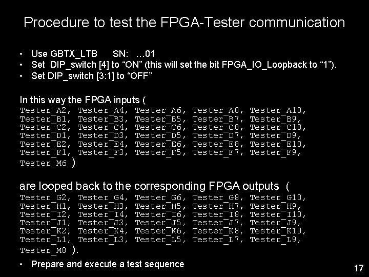
Procedure to test the FPGA-Tester communication • Use GBTX_LTB SN: … 01 • Set DIP_switch [4] to “ON” (this will set the bit FPGA_IO_Loopback to “ 1”). • Set DIP_switch [3: 1] to “OFF” In this way the FPGA inputs ( Tester_A 2, Tester_A 4, Tester_B 1, Tester_B 3, Tester_C 2, Tester_C 4, Tester_D 1, Tester_D 3, Tester_E 2, Tester_E 4, Tester_F 1, Tester_F 3, Tester_M 6 ) Tester_A 6, Tester_B 5, Tester_C 6, Tester_D 5, Tester_E 6, Tester_F 5, Tester_A 8, Tester_B 7, Tester_C 8, Tester_D 7, Tester_E 8, Tester_F 7, Tester_A 10, Tester_B 9, Tester_C 10, Tester_D 9, Tester_E 10, Tester_F 9, are looped back to the corresponding FPGA outputs ( Tester_G 2, Tester_G 4, Tester_H 1, Tester_H 3, Tester_I 2, Tester_I 4, Tester_J 1, Tester_J 3, Tester_K 2, Tester_K 4, Tester_L 1, Tester_L 3, Tester_M 8 ). Tester_G 6, Tester_H 5, Tester_I 6, Tester_J 5, Tester_K 6, Tester_L 5, • Prepare and execute a test sequence Tester_G 8, Tester_H 7, Tester_I 8, Tester_J 7, Tester_K 8, Tester_L 7, Tester_G 10, Tester_H 9, Tester_I 10, Tester_J 9, Tester_K 10, Tester_L 9, 17
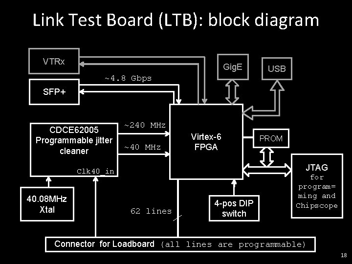
Link Test Board (LTB): block diagram VTRx Gig. E ~4. 8 Gbps USB SFP+ CDCE 62005 Programmable jitter cleaner ~240 MHz ~40 MHz Virtex-6 FPGA JTAG Clk 40_in 40. 08 MHz Xtal PROM 62 lines 4 -pos DIP switch for program= ming and Chipscope Connector for Loadboard (all lines are programmable) 18
CDCE 62005 jitter cleaner with PLL • ~0. 5 ps RMS (10 k. Hz to 20 MHz) Output Jitter Performance • Highly programmable, depending on RAM content • The RAM can be initialized by an integrated flash memory or via the SPI bus • The flash memory can be written via the SPI bus Presently on all boards, the CDCE 62005 chips: • programmed from the flash memory • ~40 MHz Clk_In (does not lock on other frequencies) • a clock output at the same frequency of Clk_In • another clock output at 6 x the frequency of Clk_In 19
Tester It needs a program (test sequence). It has a complex GUI, with many features. The present test sequence does only: • generate a 40 MHz clock • acquire and display FPGA outputs The tester could : • Execute once a finite test sequence with verification be careful with PLL locking time • Repeating the test sequence on a hardware loop no data acquisition • Repeating the test sequence on a software loop be careful with gaps in the clock; not sure about data acquisition. 20
- Slides: 20