
Stato Elettronica Mu Adriano Lai Schema della presentazione
- Slides: 16
Stato Elettronica Mu Adriano Lai Schema della presentazione • Descrizione del sistema nel suo insieme • Aspetti critici e soluzioni adottate • Componenti principali del sistema • Stato • Pianificazione CSN 1 - Lecce 24 Settembre 2003 Stato Elettronica Mu 1
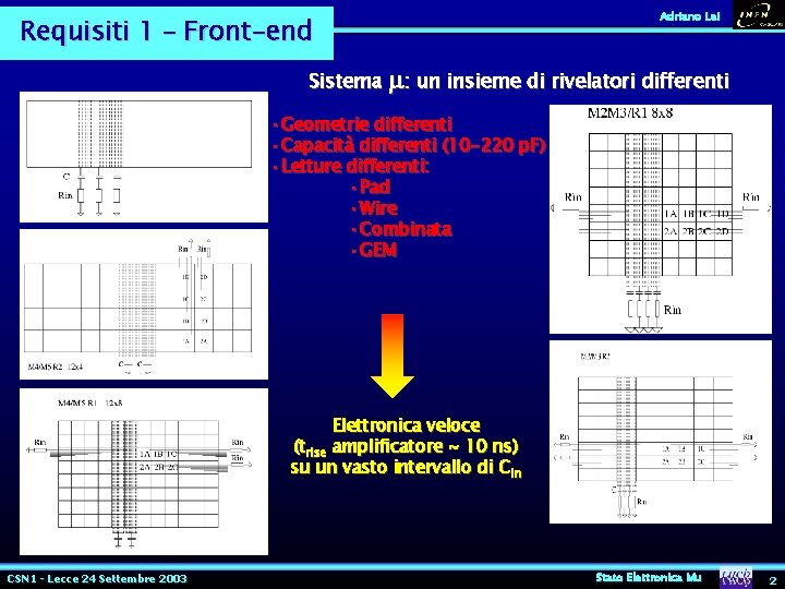
Requisiti 1 – Front-end Adriano Lai Sistema m: un insieme di rivelatori differenti • Geometrie differenti • Capacità differenti (10 -220 p. F) • Letture differenti: • Pad • Wire • Combinata • GEM Elettronica veloce (trise amplificatore ~ 10 ns) su un vasto intervallo di Cin CSN 1 - Lecce 24 Settembre 2003 Stato Elettronica Mu 2
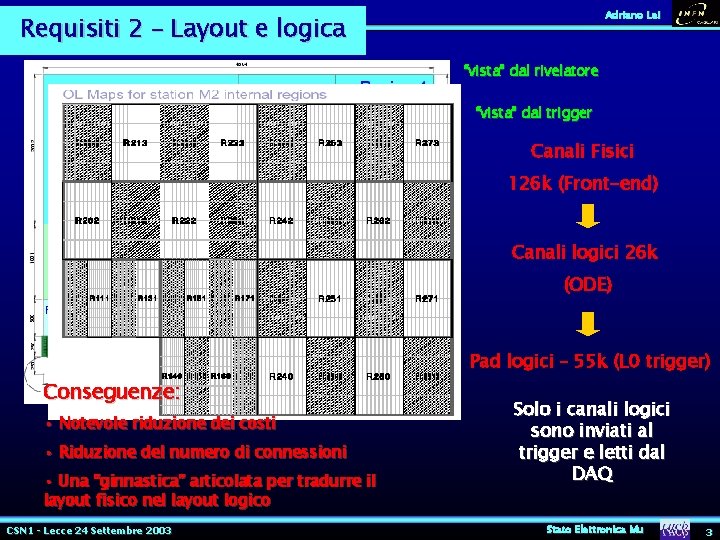
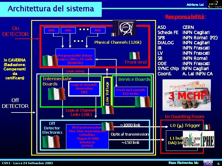
Adriano Lai Requisiti 2 – Layout e logica “vista” dal rivelatore “vista” dal trigger Canali Fisici 126 k (Front-end) Canali logici 26 k (ODE) Pad logici – 55 k (L 0 trigger) Conseguenze: • Notevole riduzione dei costi • Riduzione del numero di connessioni • Una “ginnastica” articolata per tradurre il layout fisico nel layout logico CSN 1 - Lecce 24 Settembre 2003 Solo i canali logici sono inviati al trigger e letti dal DAQ Stato Elettronica Mu 3
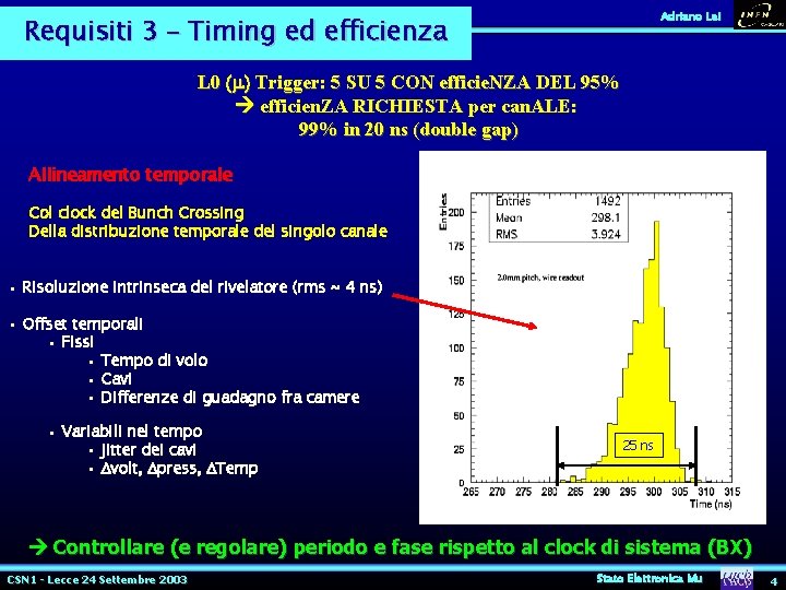
Adriano Lai Requisiti 3 – Timing ed efficienza L 0 (m) Trigger: 5 SU 5 CON efficie. NZA DEL 95% efficien. ZA RICHIESTA per can. ALE: 99% in 20 ns (double gap) Allineamento temporale Col clock del Bunch Crossing Della distribuzione temporale del singolo canale • Risoluzione intrinseca del rivelatore (rms ~ 4 ns) • Offset temporali • Fissi • Tempo di volo • Cavi • Differenze di guadagno fra camere • Variabili nel tempo • jitter dei cavi • Dvolt, Dpress, DTemp 25 ns Controllare (e regolare) periodo e fase rispetto al clock di sistema (BX) CSN 1 - Lecce 24 Settembre 2003 Stato Elettronica Mu 4
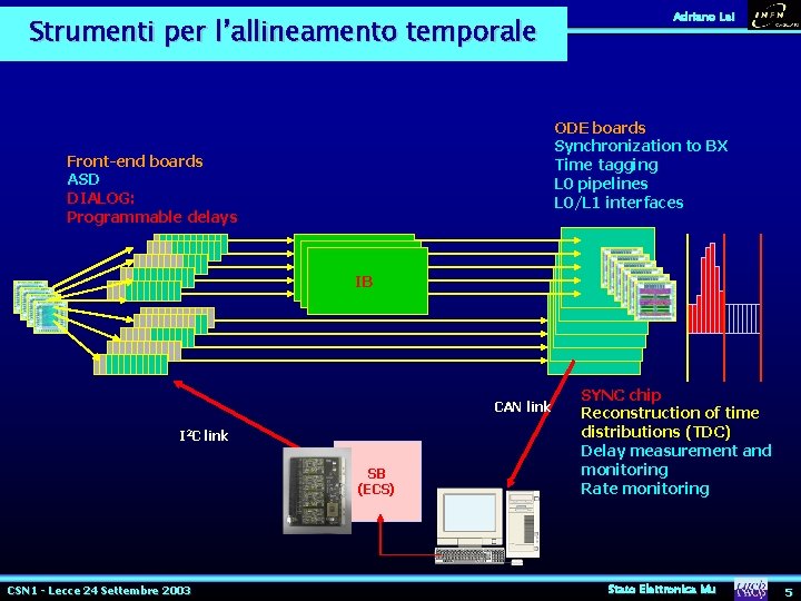
Strumenti per l’allineamento temporale Adriano Lai ODE boards Synchronization to BX Time tagging L 0 pipelines L 0/L 1 interfaces Front-end boards ASD DIALOG: Programmable delays IB CAN link I 2 C link SB (ECS) CSN 1 - Lecce 24 Settembre 2003 SYNC chip Reconstruction of time distributions (TDC) Delay measurement and monitoring Rate monitoring Stato Elettronica Mu 5
Adriano Lai Architettura del sistema On DETECTOR ASD Responsabilità: ASD Physical Channels (126 k) Front-end (42 k LVDS) Intermediate Boards Logical channels Generation (IB) Off DETECTOR Low Voltage In CAVERNA (Radiazione: Componenti da certificare) Programmable Delays Logics, DACs, I 2 C node (DIALOG) Service Boards Front-end controls ECS nodes Logical Channels Links (26 k) Off Detector Electronics CSN 1 - Lecce 24 Settembre 2003 BX Synchronization Fine Time measurement L 0 buffers Trigger & DAQ interfaces (SYNC) ASD Schede FE SPB DIALOG IB LV SB ODE SYNC chip Coord. CERN INFN Cagliari INFN Roma 1 (PZ) INFN Cagliari INFN Frascati INFN Roma 1 INFN Frascati INFN Cagliari A. Lai INFN CA 3 MCHF In Counting Room ~1000 link Optical transmission ~150 link L 0 (m) Trigger L 1 buffers & DAQ Interface Stato Elettronica Mu 6
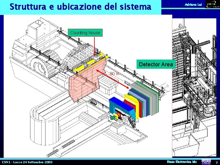
Struttura e ubicazione del sistema Adriano Lai Muon filters Crates Counting house Detector Area M 2 -M 5 80 m Camere CSN 1 - Lecce 24 Settembre 2003 Stato Elettronica Mu 7
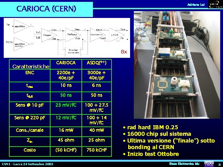
Adriano Lai CARIOCA (CERN) 8 x CARIOCA ASDQ(++) ENC 2200 e + 40 e/p. F 3000 e + 40 e/p. F trise 10 ns 6 ns tfall 50 ns Sens @ 10 p. F 23 m. V/f. C 100 + 27. 5 m. V/f. C Sens @ 220 p. F 12 m. V/f. C 100 + 14 m. V/f. C Cons. /canale 16 m. W 40 m. W Zin 45 ohm 25 ohm Costo (50 k. CHF) 750 k. CHF Caratteristiche CSN 1 - Lecce 24 Settembre 2003 • rad hard IBM 0. 25 • 16000 chip sul sistema • Ultima versione (“finale”) sotto bonding al CERN • Inizio test Ottobre Stato Elettronica Mu 8
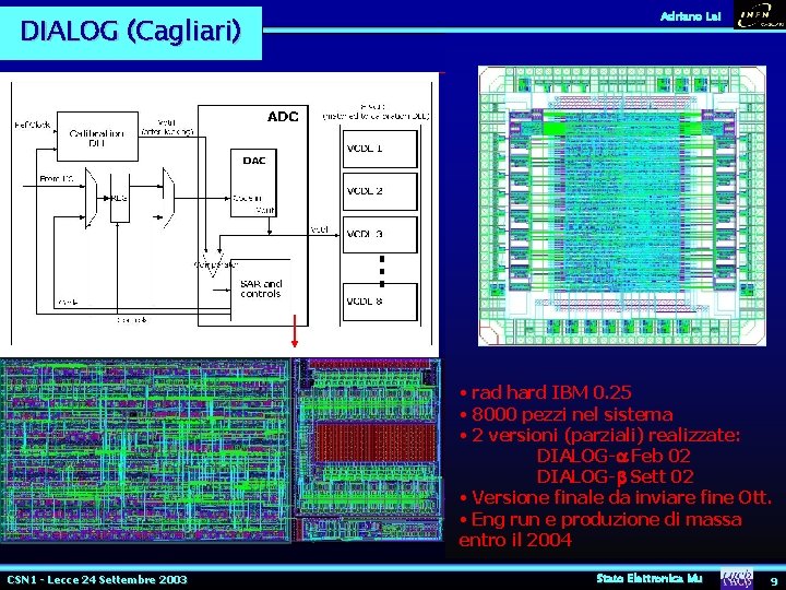
Adriano Lai DIALOG (Cagliari) ü 16 LVDS input Prog. Delayer Prog. Dig. Shaper M A S K Logical Channel Generation 8 LVDS output CAlib. DLL & DLL ADC ü ü Calibration CLK 16 bits Rate counter SCL I 2 C Interface Start/Stop DIALOG Configuration registers SDA Address Pls 0 ASD pulse generation & Delay Pulse Pls 1 Threshold 1 -16 Thr DAC 1 -16 CSN 1 - Lecce 24 Settembre 2003 ü ü Tst Signal Programmable time adjustment (32 steps of ~1. 5 ns each @40 MHz) with external calibration by DLL (settable period ~ 40 -15 ns) Programmable output signal width adjustment (8 steps of ~3 ns each) Mask on every input channel 16 DACs for ASD threshold settings: LSB ~ 0. 1 f. C @ 10 p. F, ~ 0. 2 f. C @ 220 p. F 2 I C Interface Triple-voted and auto-corrected registers for better SEU immunity (both configuration and state machines) Logical Channel generation: Ø OR 2 ; OR 4 ; OR 8 Ø AND 2 ; OR 2 (2 AND 2) ; OR 4 (4 AND 2) • rad hard IBM 0. 25 ü ASD pulse generation • ü 8000 pezzi nel sistema 16 bits rate counter (1 channel at a time) • ü 2 Internal versioni (parziali) realizzate: Pattern generation DIALOG-a Feb 02 DIALOG-b Sett 02 • Versione finale da inviare fine Ott. • Eng run e produzione di massa entro il 2004 Stato Elettronica Mu 9
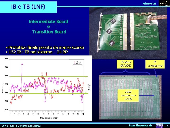
Adriano Lai IB e TB (LNF) Intermediate Board e Transition Board • Prototipo finale pronto da marzo scorso • 152 IB+TB nel sistema – 24 BP 16 16 slots (IB/ODE) OR 4 A OR 4 B OR 24 A OR 24 B PS connectors 15 2 ns window Time [nsec] 15. 5 14 CAN connectors (ODE) 13. 5 13 10 20 30 40 50 60 70 80 90 Input channel number CSN 1 - Lecce 24 Settembre 2003 Stato Elettronica Mu 10
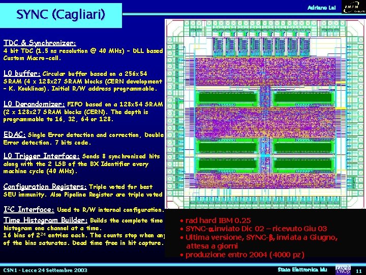
Adriano Lai SYNC (Cagliari) From DIALOG/IB 8 LVDS in TDC & Synchronizer: 4 bit TDC (1. 5 ns resolution @ 40 MHz) – DLL based To GOL Custom Macro-cell. L 0 buffer: Circular buffer based on a 256 x 54 SRAM (4 x 128 x 27 SRAM blocks (CERN development – K. Kouklinas). Initial R/W address programmable. L 0 Derandomizer: FIFO based on a 128 x 54 SRAM 4 bits x 8 Phase 4 bits x 8 Prog GOL buffer BX sync BX + hits 4+8 Phase 4 bits x 8 Error detection. 7 bits code. L 0 Trigger Interface: Sends 8 synchronized hits along with the 2 LSB of the BX Identifier every machine cycle (40 MHz). 24 bits x 16 BX count BX 4 bit from/to SB Hamming code generator (2 x 128 x 27 SRAM blocks (CERN). The depth is programmable to 16, 32, 64 or 128. EDAC: Single Error detection and correction, Double Fine Time Histogram FT L 0 buffer DPRAM 256 x 54 EDAC I 2 C interface SCL SDA SYNC Configuration registers EV count ERR flags EV 4 bit Hamming code generator Configuration Registers: Triple voted for best SEU immunity. Also Pipeline Register are triple voted I 2 C Interface: Used to R/W internal configuration. Time Histogram Builder: Builds the complete time histogram one channel at a time. 16 bins of 224 entries each. The counts stop when any of the bins saturates. Dead time free in hit capture. CSN 1 - Lecce 24 Settembre 2003 L 0 derandomizer DPRAM 128 x 54 ERR flags • rad hard IBM 0. 25 EDAC • SYNC-a inviato Dic 02 – ricevuto Giu 03 Out. Mux 32 xa 2 Giugno, • Ultima versione, SYNC-b, inviata attesa a giorni To L 1 • produzione entro 2004 (4000 pz) Stato Elettronica Mu 11
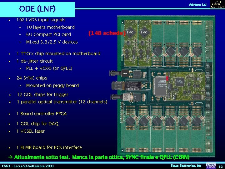
Adriano Lai ODE (LNF) • 192 LVDS input signals – 10 layers motherboard – 6 U Compact PCI card – Mixed 3. 3/2. 5 V devices (148 schede) • 1 TTCrx chip mounted on motherboard • 1 de-jitter circuit – PLL + VCXO (or QPLL) VCsel • 24 SYNC chips – Mounted on piggy board • 12 GOL chips for trigger • 1 parallel optical transmitter (12 channels) • 1 Board controller FPGA • 1 GOL chip for DAQ • 1 VCSEL laser • 1 ELMB board for ECS interface Attualmente sotto test. Manca la parte ottica, SYNC finale e QPLL (CERN) CSN 1 - Lecce 24 Settembre 2003 Stato Elettronica Mu 12
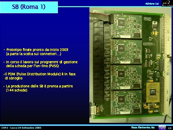
Adriano Lai SB (Roma 1) SCL SDA_IN SDA_OUT Test/Pulse RESET CANBUS ELMB • Prototipo finale pronto da inizio 2003 (a parte la scelta sui connettori…) • In corso il lavoro sui programmi di gestione della scheda per l’on-line (PVSS) • Il PDM (Pulse Distribution Module) è in fase di sbroglio • La produzione delle SB è pronta a partire (144 schede)CLK 40 test BC Pulse pulse logic Test/pulse 2 3 1 ELMB Test/pulse 2 3 3 x LVDS I 2 c each ELMB 1 ELMB Test/pulse CSN 1 - Lecce 24 Settembre 2003 1 2 ttl/lvds converter 3 Stato Elettronica Mu 13
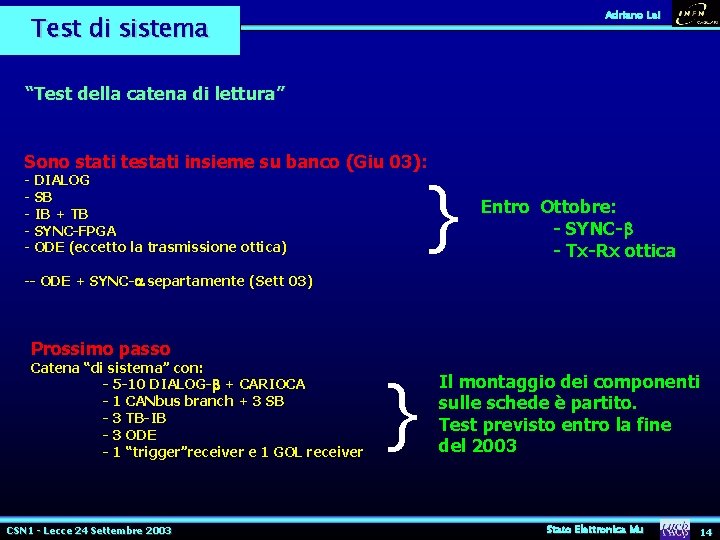
Adriano Lai Test di sistema “Test della catena di lettura” Sono stati testati insieme su banco (Giu 03): } - DIALOG - SB - IB + TB - SYNC-FPGA - ODE (eccetto la trasmissione ottica) Entro Ottobre: - SYNC-b - Tx-Rx ottica -- ODE + SYNC-a separtamente (Sett 03) Prossimo passo Catena “di sistema” con: - 5 -10 DIALOG-b + CARIOCA - 1 CANbus branch + 3 SB - 3 TB-IB - 3 ODE - 1 “trigger”receiver e 1 GOL receiver CSN 1 - Lecce 24 Settembre 2003 } Il montaggio dei componenti sulle schede è partito. Test previsto entro la fine del 2003 Stato Elettronica Mu 14
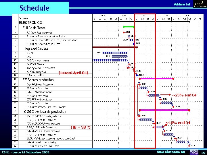
Adriano Lai Schedule (moved April 04) ~25% end 04 ~10% end 04 (IB + SB ? ) CSN 1 - Lecce 24 Settembre 2003 Stato Elettronica Mu 15
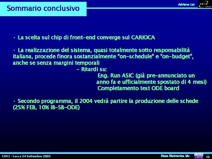
Sommario conclusivo Adriano Lai • La scelta sul chip di front-end converge sul CARIOCA • La realizzazione del sistema, quasi totalmente sotto responsabilità italiana, procede finora sostanzialmente “on-schedule” e “on-budget”, anche se senza margini temporali - Ritardi su: Eng. Run ASIC (già pre-annunciato un anno fa e ufficialmente spostato di 4 mesi) Completamento test ODE board • Secondo programma, il 2004 vedrà partire la produzione delle schede (25% FEB, 10% IB-SB-ODE) CSN 1 - Lecce 24 Settembre 2003 Stato Elettronica Mu 16