State of the Art in Microelectronics Miniaturization and


![Advances in ADCs 1 E+07 1 E+06 P/fsnyq [p. J] Courtesy of Prof. Advances in ADCs 1 E+07 1 E+06 P/fsnyq [p. J] Courtesy of Prof.](https://slidetodoc.com/presentation_image_h/1e854c8b81ffd7e1cdf65c684a35ad38/image-28.jpg)



- Slides: 47

State of the Art in Microelectronics Miniaturization and Integration Microelectronics for Particle Detectors A. Marchioro CERN, Div. PH 1211 Geneva 23, Switzerland

Overview u Motivations: i. e. the talk’s message: – Experiments require systems, not chips u Brief intro on technology perspectives – History – Technologies for So. C – Advanced Devices for Billion transistor chips u Opportunities: – So. Cs for gas detectors – So. Cs for trackers u Conclusions A. Marchioro - MPGD 2013 2

MOTIVATIONS - History of m. Electronics for HEP vs Commercial Areas with potential for growth A. Marchioro - MPGD 2013 3

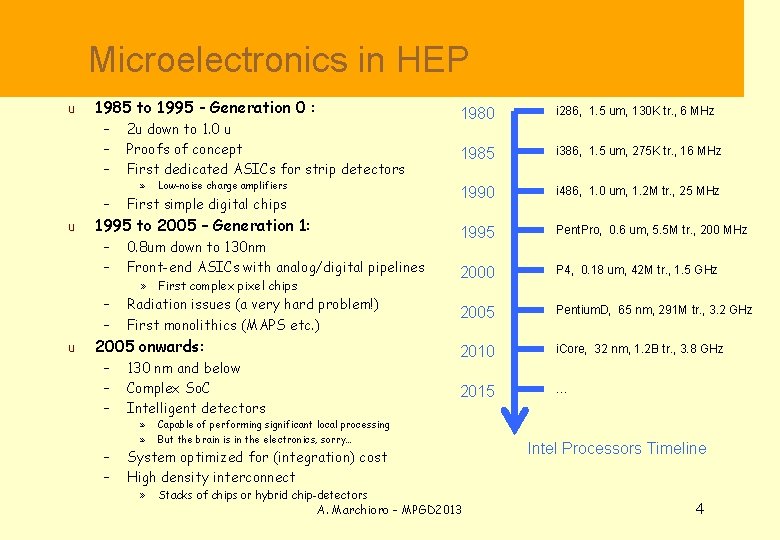
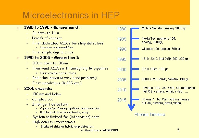
Microelectronics in HEP u 1985 to 1995 - Generation 0 : – – u u 2 u down to 1. 0 u Proofs of concept First dedicated ASICs for strip detectors » Low-noise charge amplifiers First simple digital chips 1995 to 2005 – Generation 1: – – 0. 8 um down to 130 nm Front-end ASICs with analog/digital pipelines – – Radiation issues (a very hard problem!) First monolithics (MAPS etc. ) » First complex pixel chips 2005 onwards: – – – 130 nm and below Complex So. C Intelligent detectors » » 1980 i 286, 1. 5 um, 130 K tr. , 6 MHz 1985 i 386, 1. 5 um, 275 K tr. , 16 MHz 1990 i 486, 1. 0 um, 1. 2 M tr. , 25 MHz 1995 Pent. Pro, 0. 6 um, 5. 5 M tr. , 200 MHz 2000 P 4, 0. 18 um, 42 M tr. , 1. 5 GHz 2005 Pentium. D, 65 nm, 291 M tr. , 3. 2 GHz 2010 i. Core, 32 nm, 1. 2 B tr. , 3. 8 GHz 2015 … Capable of performing significant local processing But the brain is in the electronics, sorry… System optimized for (integration) cost High density interconnect » Stacks of chips or hybrid chip-detectors A. Marchioro - MPGD 2013 Intel Processors Timeline 4

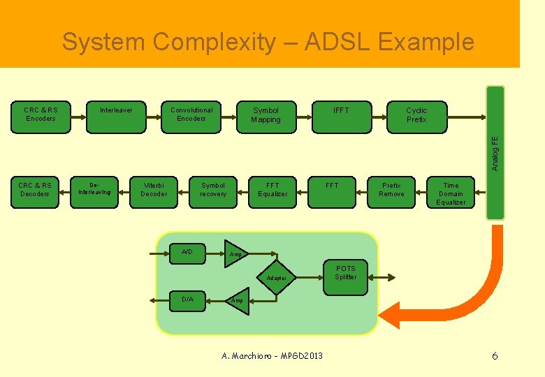
Microelectronics in HEP u 1985 to 1995 - Generation 0 : – – u u 2 u down to 1. 0 u Proofs of concept First dedicated ASICs for strip detectors » Low-noise charge amplifiers First simple digital chips 1995 to 2005 – Generation 1: – – 0. 8 um down to 130 nm Front-end ASICs with analog/digital pipelines – – Radiation issues (a very hard problem!) First monolithics (MAPS etc. ) » First complex pixel chips 2005 onwards: – – – 130 nm and below Complex So. C Intelligent detectors » » 1980 Mobira Senator, analog, 9800 gr 1985 Nokia Technophone 105, analog, 5500 gr, 1990 Cityman 100, analog, 500 gr 1995 1610, 2210, first GSM 900, 230 gr, 2000 3310, GSM, 130 gr 2005 8800, GMS, WAP, camera, 130 gr 2010 2015 Capable of performing significant local processing But the brain is in the electronics, sorry… System optimized for (integration) cost High density interconnect » Stacks of chips or hybrid chip-detectors A. Marchioro - MPGD 2013 i. Phone 3 GS , 3 G, Wi. Fi, GB memories, full OS, camera, email, video, … i. Phone 7 , 4 G, Wi. Fi, GB memories, full OS, camera, email, video, … Phones Timeline 5

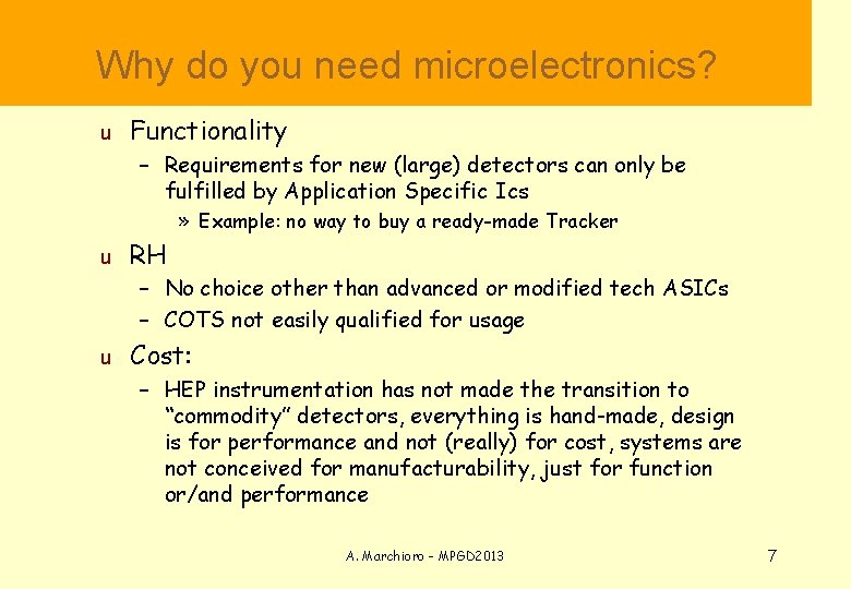
System Complexity – ADSL Example Interleaver Convolutional Encoders Symbol Mapping IFFT Cyclic Prefix Analog FE CRC & RS Encoders CRC & RS Decoders Deinterleaving Viterbi Decoder Symbol recovery A/D FFT Equalizer Prefix Remove Time Domain Equalizer Amp Adapter D/A FFT POTS Splitter Amp A. Marchioro - MPGD 2013 6

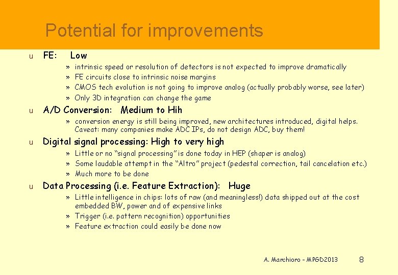
Why do you need microelectronics? u Functionality – Requirements for new (large) detectors can only be fulfilled by Application Specific Ics » Example: no way to buy a ready-made Tracker u RH – No choice other than advanced or modified tech ASICs – COTS not easily qualified for usage u Cost: – HEP instrumentation has not made the transition to “commodity” detectors, everything is hand-made, design is for performance and not (really) for cost, systems are not conceived for manufacturability, just for function or/and performance A. Marchioro - MPGD 2013 7

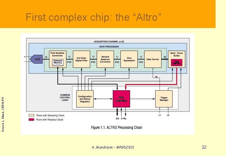
Potential for improvements u u FE: » » Low intrinsic speed or resolution of detectors is not expected to improve dramatically FE circuits close to intrinsic noise margins CMOS tech evolution is not going to improve analog (actually probably worse, see later) Only 3 D integration can change the game A/D Conversion: Medium to Hih » conversion energy is still being improved, new architectures introduced, digital helps. Caveat: many companies make ADC IPs, do not design ADC, buy them! u Digital signal processing: High to very high » Little or no “signal processing” is done today in HEP (shaper is analog) » Some laudable attempt in the “Altro” project (pedestal correction, tail cancelation etc. ) » Much more to be done u Data Processing (i. e. Feature Extraction): Huge » Little intelligence in chips: lots of raw (and meaningless!) data shipped out at the cost embedded BW, power and of expensive links » Trigger (i. e. pattern recognition) opportunities » Feature extraction could easily be done now A. Marchioro - MPGD 2013 8

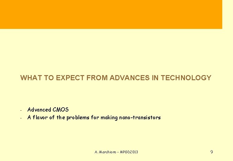
WHAT TO EXPECT FROM ADVANCES IN TECHNOLOGY - Advanced CMOS A flavor of the problems for making nano-transistors A. Marchioro - MPGD 2013 9

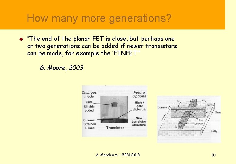
How many more generations? u “The end of the planar FET is close, but perhaps one or two generations can be added if newer transistors can be made, for example the ‘FINFET’” G. Moore, 2003 A. Marchioro - MPGD 2013 10

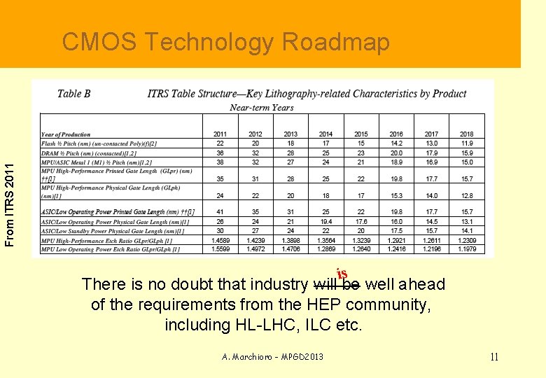
CMOS Technology Roadmap From ITRS 2011 is There is no doubt that industry will be well ahead of the requirements from the HEP community, including HL-LHC, ILC etc. A. Marchioro - MPGD 2013 11

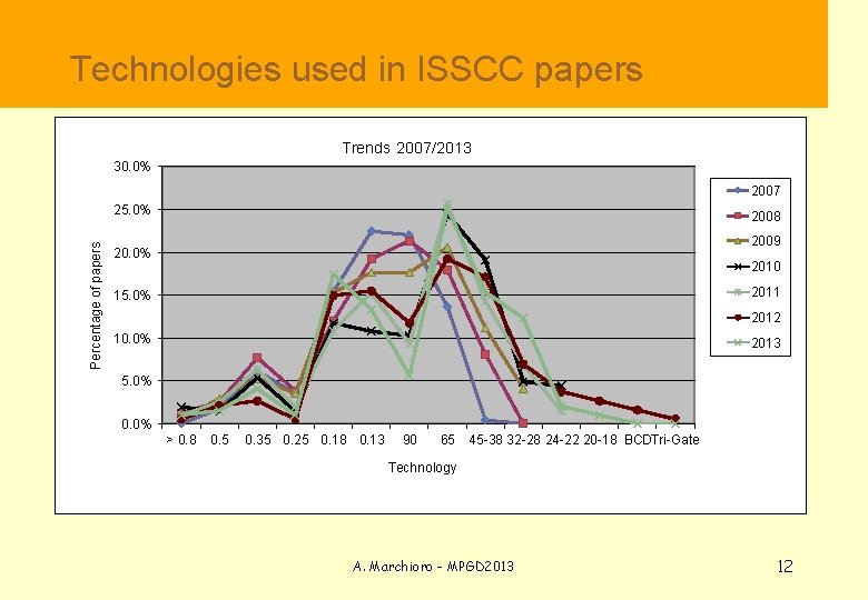
Technologies used in ISSCC papers Trends 2007/2013 30. 0% 2007 Percentage of papers 25. 0% 2008 2009 20. 0% 2010 2011 15. 0% 2012 10. 0% 2013 5. 0% 0. 0% > 0. 8 0. 5 0. 35 0. 25 0. 18 0. 13 90 65 45 -38 32 -28 24 -22 20 -18 BCDTri-Gate Technology A. Marchioro - MPGD 2013 12

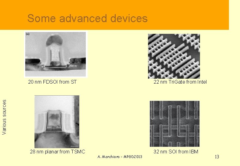
Some advanced devices 22 nm Tri. Gate from Intel Various sources 20 nm FDSOI from ST 28 nm planar from TSMC A. Marchioro - MPGD 2013 32 nm SOI from IBM 13

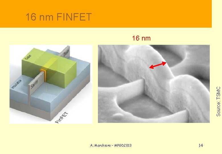
16 nm FINFET Source: TSMC 16 nm A. Marchioro - MPGD 2013 14

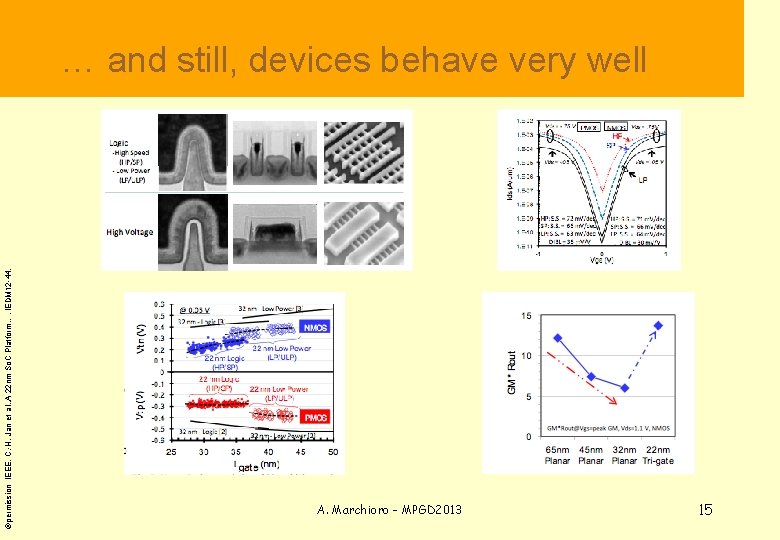
… and still, devices behave very well ©permission IEEE, C. -H. Jan et al. , A 22 nm So. C Platform…, IEDM 12 -44, A. Marchioro - MPGD 2013 15

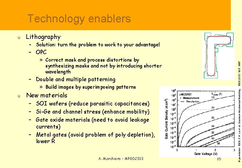
Technology enablers u Lithography – Solution: turn the problem to work to your advantage! » Correct mask and process distortions by synthesizing masks and not by introducing shorter wavelength – Double and multiple patterning » Build images by superimposing patterns u New materials – SOI wafers (reduce parasitic capacitances) – Si-Ge and channel stress (enhance mobility) – Gate oxide materials (need to avoid leakage currents) – Metal gates (avoid problem of poly depletion), lower R A. Marchioro - MPGD 2013 16 © permission IEEE, S. H. Lo et al. , Quantum-Mechanical Modeling… IEEE JSSC 18, 5, 1997 – OPC

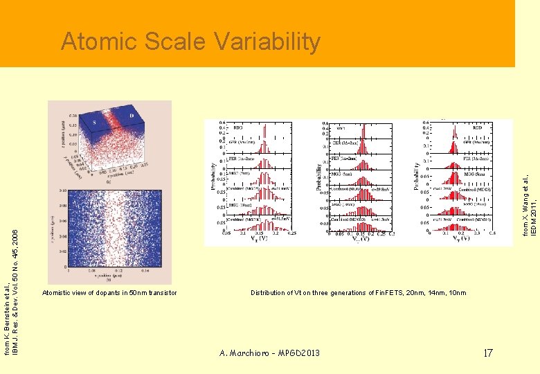
Atomic Scale Variability from X. Wang et al. , IEDM 2011, from K. Bernstein et al. , IBM J. Res. & Dev. Vol. 50 No. 4/5, 2006 Atomistic view of dopants in 50 nm transistor Distribution of Vt on three generations of Fin. FETS, 20 nm, 14 nm, 10 nm A. Marchioro - MPGD 2013 17

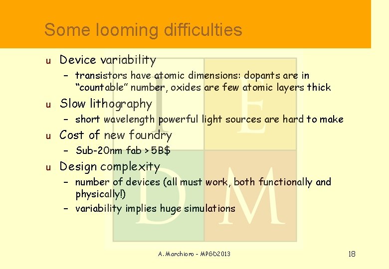
Some looming difficulties u Device variability – transistors have atomic dimensions: dopants are in “countable” number, oxides are few atomic layers thick u Slow lithography – short wavelength powerful light sources are hard to make u Cost of new foundry – Sub-20 nm fab > 5 B$ u Design complexity – number of devices (all must work, both functionally and physically!) – variability implies huge simulations A. Marchioro - MPGD 2013 18

IMPORTANT BENEFITS FROM NEW TECHNOLOGIES 130 and 65 nm and Radiation hardness A. Marchioro - MPGD 2013 19

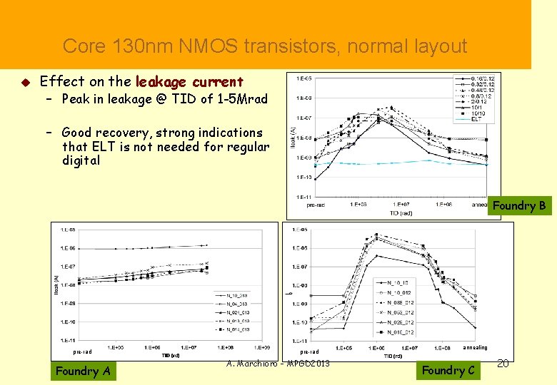
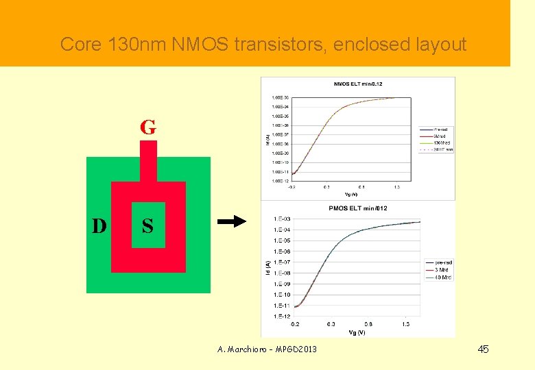
Core 130 nm NMOS transistors, normal layout u Effect on the leakage current – Peak in leakage @ TID of 1 -5 Mrad – Good recovery, strong indications that ELT is not needed for regular digital Foundry B pre-rad Foundry A pre-rad A. Marchioro - MPGD 2013 annealing Foundry C 20

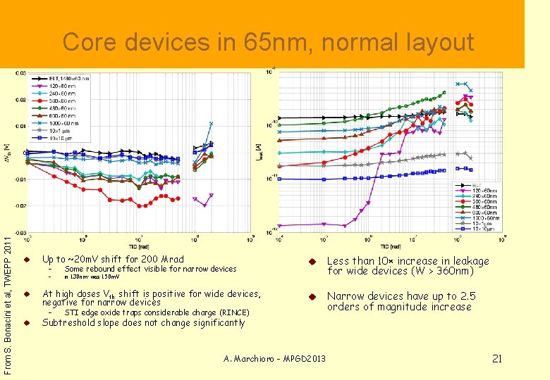
Core devices in 65 nm, normal layout From S. Bonacini et al, TWEPP 2011 u Up to ~20 m. V shift for 200 Mrad – – u u Less than 10× increase in leakage for wide devices (W > 360 nm) u Narrow devices have up to 2. 5 orders of magnitude increase in 130 nm: was 150 m. V At high doses Vth shift is positive for wide devices, negative for narrow devices – u Some rebound effect visible for narrow devices STI edge oxide traps considerable charge (RINCE) Subtreshold slope does not change significantly A. Marchioro - MPGD 2013 21

OTHER BENEFITS FROM NEW TECHNOLOGIES Size, functionality and features A. Marchioro - MPGD 2013 22

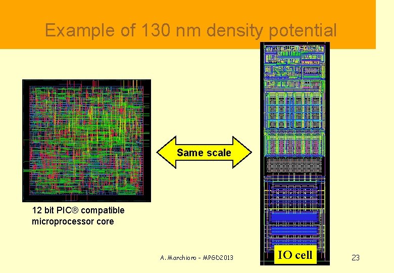
Example of 130 nm density potential Same scale 12 bit PIC® compatible microprocessor core A. Marchioro - MPGD 2013 IO cell 23

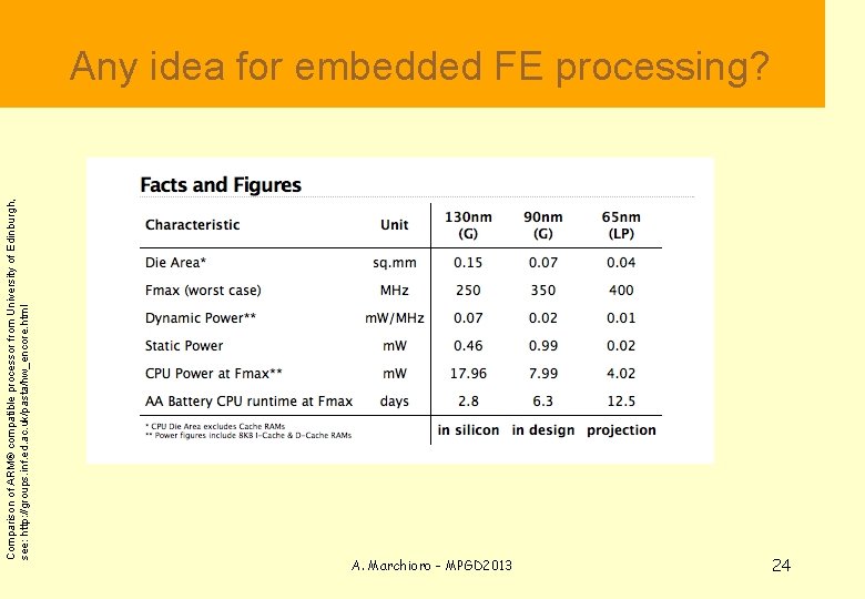
Comparison of ARM® compatible processor from University of Edinburgh, see: http: //groups. inf. ed. ac. uk/pasta/hw_encore. html Any idea for embedded FE processing? A. Marchioro - MPGD 2013 24

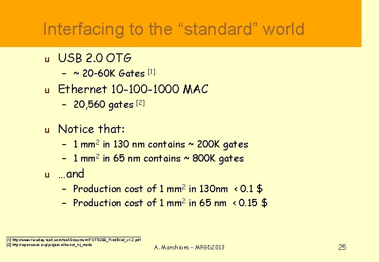
Interfacing to the “standard” world u USB 2. 0 OTG – ~ 20 -60 K Gates [1] u Ethernet 10 -1000 MAC – 20, 560 gates [2] u Notice that: – 1 mm 2 in 130 nm contains ~ 200 K gates – 1 mm 2 in 65 nm contains ~ 800 K gates u …and – Production cost of 1 mm 2 in 130 nm < 0. 1 $ – Production cost of 1 mm 2 in 65 nm < 0. 15 $ _______________________________ [1] http: //www. faraday-tech. com/tech. Document/FOTG 200_Prod. Brief_v 1. 2. pdf [2] http: //opencores. org/project, ethernet_tri_mode A. Marchioro - MPGD 2013 25

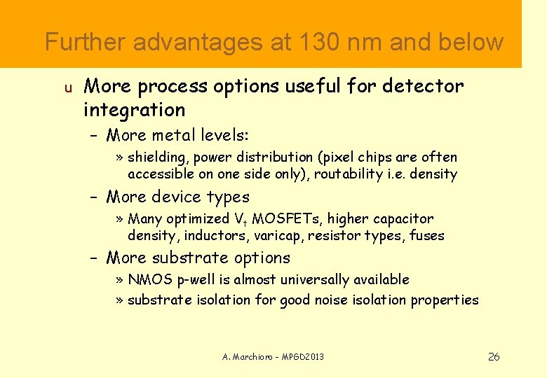
Further advantages at 130 nm and below u More process options useful for detector integration – More metal levels: » shielding, power distribution (pixel chips are often accessible on one side only), routability i. e. density – More device types » Many optimized Vt MOSFETs, higher capacitor density, inductors, varicap, resistor types, fuses – More substrate options » NMOS p-well is almost universally available » substrate isolation for good noise isolation properties A. Marchioro - MPGD 2013 26

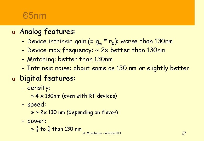
65 nm u Analog features: – – u Device intrinsic gain (= gm * r 0): worse than 130 nm Device max frequency: ~ 2 x better than 130 nm Matching: better than 130 nm Intrinsic noise: about same as 130 nm or slightly better Digital features: – density: » 4 x 130 nm (even with RT devices) – speed: » ~ 2 x 130 nm (depending on flavor) – power: » ½ to ¼ than 130 nm A. Marchioro - MPGD 2013 27
![Advances in ADCs 1 E07 1 E06 Pfsnyq p J Courtesy of Prof Advances in ADCs 1 E+07 1 E+06 P/fsnyq [p. J] Courtesy of Prof.](https://slidetodoc.com/presentation_image_h/1e854c8b81ffd7e1cdf65c684a35ad38/image-28.jpg)
Advances in ADCs 1 E+07 1 E+06 P/fsnyq [p. J] Courtesy of Prof. B. Murmann, Stanford University 1 E+05 1 E+04 1 E+03 1 E+02 ISSCC 2013 VLSI 2012 ISSCC 1997 -2012 VLSI 1997 -2011 FOMW=10 f. J/conv-step FOMS=170 d. B 1 E+01 1 E+00 1 E-01 10 20 30 40 50 60 70 80 90 100 110 120 SNDR @ Nyquist [d. B] A. Marchioro - MPGD 2013 28

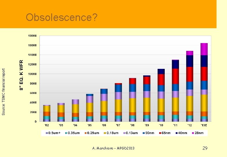
Obsolescence? Source: TSMC financial report A. Marchioro - MPGD 2013 29

OPPORTUNITIES: - Chips for gas detectors - Chips for trackers A. Marchioro - MPGD 2013 30

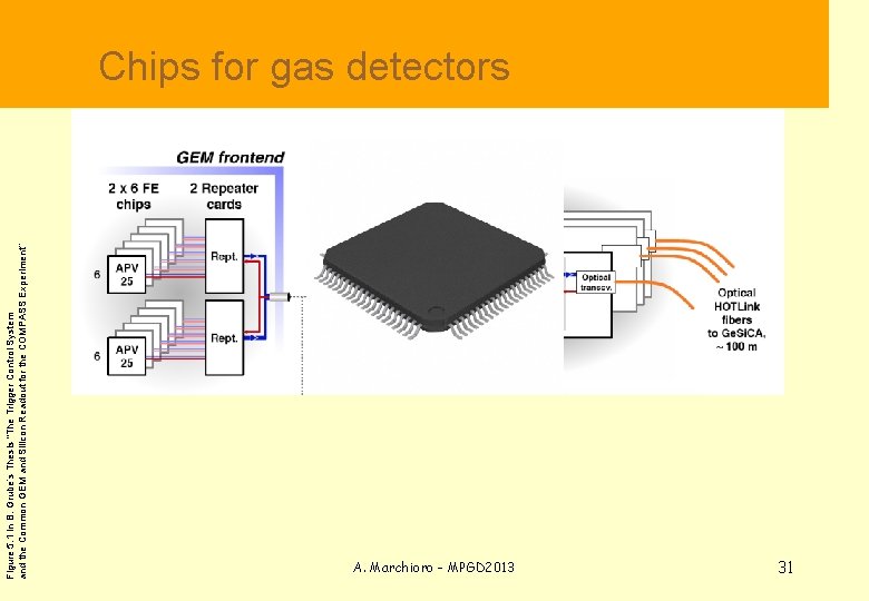
Figure 5. 1 in B. Grube’s Thesis “The Trigger Control System and the Common GEM and Silicon Readout for the COMPASS Experiment” Chips for gas detectors A. Marchioro - MPGD 2013 31

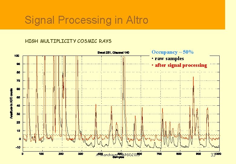
First complex chip: the “Altro” Source L. Musa, CERN-PH A. Marchioro - MPGD 2013 32

Signal Processing in Altro HIGH MULTIPLICITY COSMIC RAYS Occupancy ~ 50% • raw samples • after signal processing A. Marchioro - MPGD 2013 33

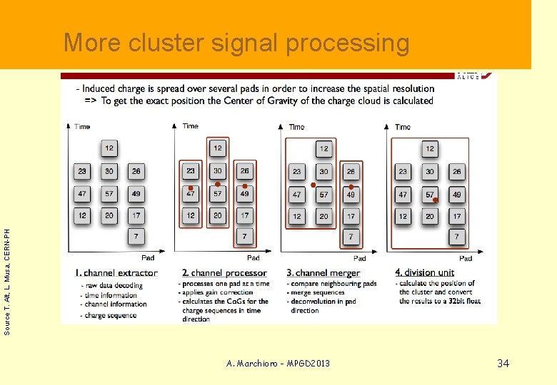
More cluster signal processing Source T. Alt, L. Musa, CERN-PH A. Marchioro - MPGD 2013 34

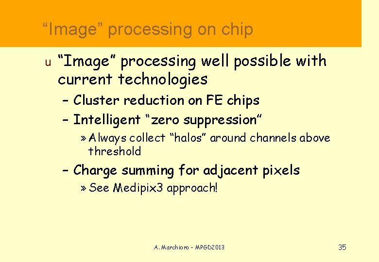
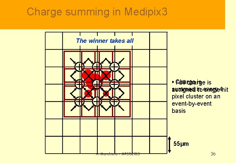
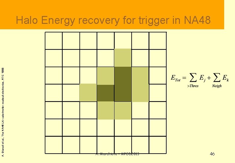
“Image” processing on chip u “Image” processing well possible with current technologies – Cluster reduction on FE chips – Intelligent “zero suppression” » Always collect “halos” around channels above threshold – Charge summing for adjacent pixels » See Medipix 3 approach! A. Marchioro - MPGD 2013 35

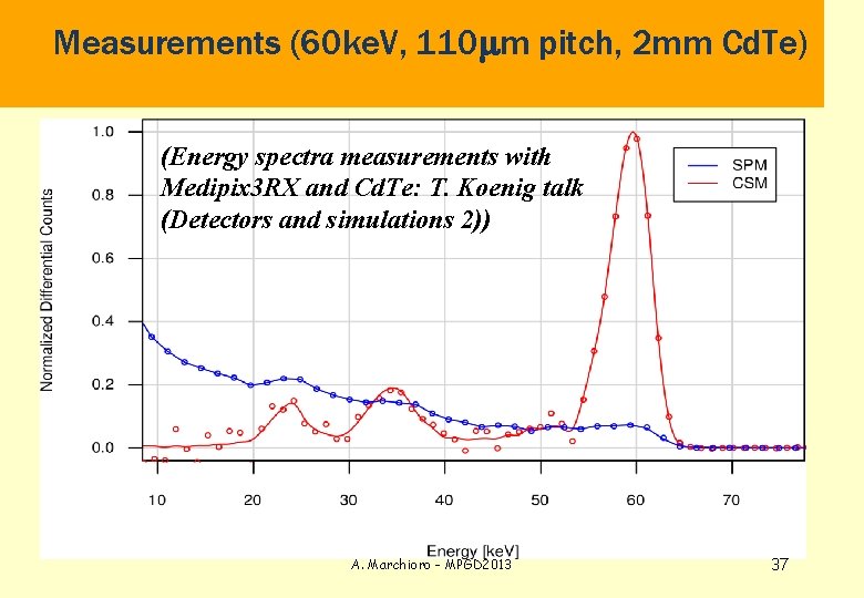
Charge summing in Medipix 3 The winner takes all Charge is is • Full charge summed in assigned to every single 4 hit pixel cluster on an event-by-event basis 55µm A. Marchioro - MPGD 2013 36

Measurements (60 ke. V, 110 mm pitch, 2 mm Cd. Te) (Energy spectra measurements with Medipix 3 RX and Cd. Te: T. Koenig talk (Detectors and simulations 2)) A. Marchioro - MPGD 2013 37

Chips for Trackers A. Marchioro - MPGD 2013 38

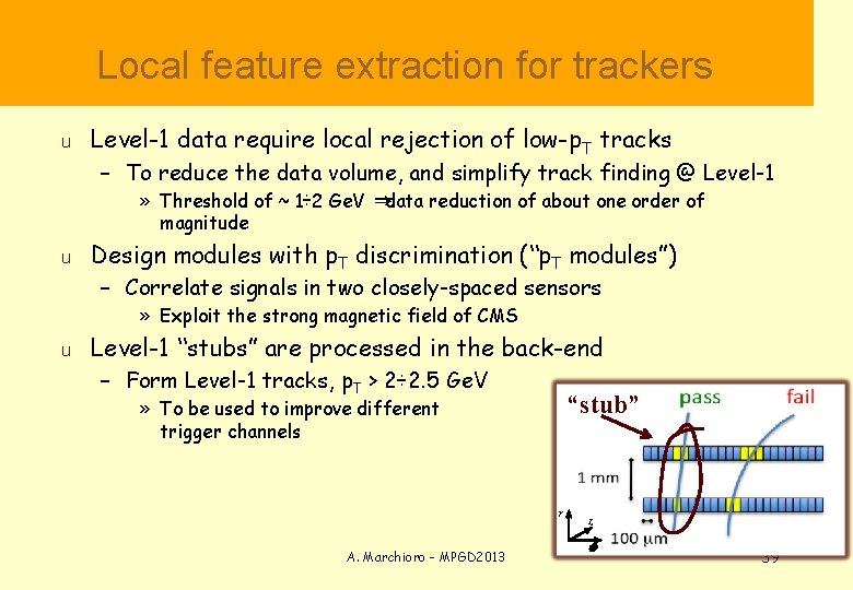
Local feature extraction for trackers u Level-1 data require local rejection of low-p. T tracks – To reduce the data volume, and simplify track finding @ Level-1 » Threshold of ~ 1÷ 2 Ge. V ⇒data reduction of about one order of magnitude u Design modules with p. T discrimination (“p. T modules”) – Correlate signals in two closely-spaced sensors » Exploit the strong magnetic field of CMS u Level-1 “stubs” are processed in the back-end – Form Level-1 tracks, p. T > 2÷ 2. 5 Ge. V “stub” » To be used to improve different trigger channels r A. Marchioro - MPGD 2013 z F 39

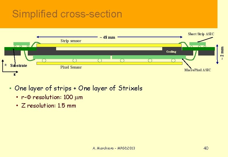
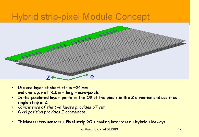
Simplified cross-section ~ 2 mm Strip sensor Short Strip ASIC ~ 48 mm Cooling R Substrate Pixel Sensor Macro. Pixel ASIC Z • One layer of strips + One layer of Strixels • r-F resolution: 100 mm • Z resolution: 1. 5 mm A. Marchioro - MPGD 2013 40

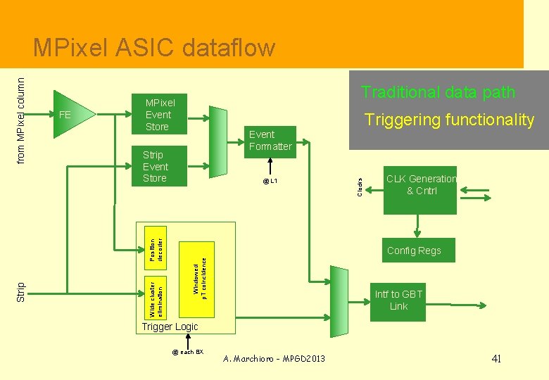
Triggering functionality @ L 1 Clocks Event Formatter Strip Event Store Wide cluster elimination Strip Traditional data path MPixel Event Store Position decoder from MPixel column FE ASIC dataflow CLK Generation & Cntrl Config Regs Windowed p. T coincidence MPixel Intf to GBT Link Trigger Logic @ each BX A. Marchioro - MPGD 2013 41

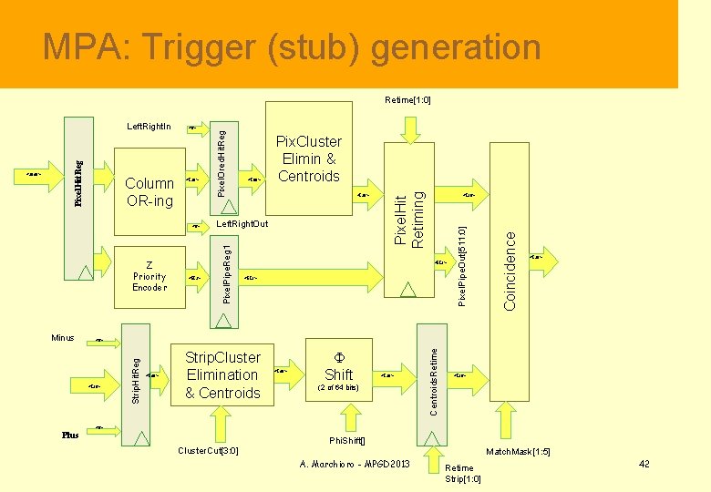
MPA: Trigger (stub) generation Z Priority Encoder Left. Right. Out <128> <512> <128> <140> Strip. Cluster Elimination & Centroids <140> F Shift <128> (2 of 64 bits) Centroids. Retime Minus <512> <128> Coincidence <8> <136> Pixel. Pipe. Out[511: 0] <128> Pix. Cluster Elimin & Centroids Pixel. Hit Retiming <8> Pixel. Pipe. Reg 1 Column OR-ing Strip. Hit. Reg <2048> Pixel. Hit. Reg Left. Right. In Pixel. Ored. Hit. Reg Retime[1: 0] <128> <8> Plus Phi. Shift[] Cluster. Cut[3: 0] Match. Mask[1: 5] A. Marchioro - MPGD 2013 Retime Strip[1: 0] 42

Conclusions u Development is limited by (lack of) ideas, not by technology – … and not even by the “cost” of adv tech u u The HEP community has much to learn, (and to profit from) adopting standards, IP sharing, and avoiding NIH attitudes Detectors and microelectronics should be developed in parallel – much to be expected from jointly conceived So. C for detectors A. Marchioro - MPGD 2013 43

Spares A. Marchioro - MPGD 2013 44

Core 130 nm NMOS transistors, enclosed layout G D S A. Marchioro - MPGD 2013 45

A. Gianoli et al. , The NA 48 LKr calorimeter readout electronics, RTC 1999 Halo Energy recovery for trigger in NA 48 A. Marchioro - MPGD 2013 46

Hybrid strip-pixel Module Concept Z f • • Use one layer of short strip: ~24 mm and one layer of ~1. 5 mm long macro-pixels In the pixelated layer, perform the OR of the pixels in the Z direction and use it as single strip in Z Coincidence of the two layers provides p. T cut Pixel position provides Z coordinate • Thickness: two sensors + Pixel strip RO + cooling interposer + hybrid sideways • • A. Marchioro - MPGD 2013 47