STABILITY ANALYSIS OF CMOS BASED SUBTHRESHOLD SRAM CIRCUITS

STABILITY ANALYSIS OF CMOS BASED SUBTHRESHOLD SRAM CIRCUITS NARAYAN AIYER VENKATESAN ELECTRICAL ENGINEERING
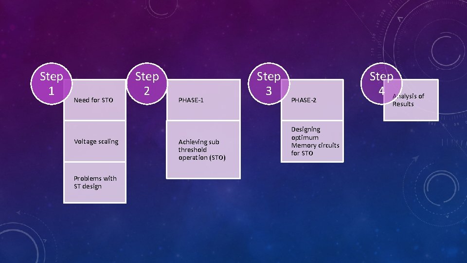
Step 1 Need for STO Voltage scaling Problems with ST design Step 2 PHASE-1 Achieving sub threshold operation (STO) Step 3 PHASE-2 Designing optimum Memory circuits for STO Step 4 Analysis of Results
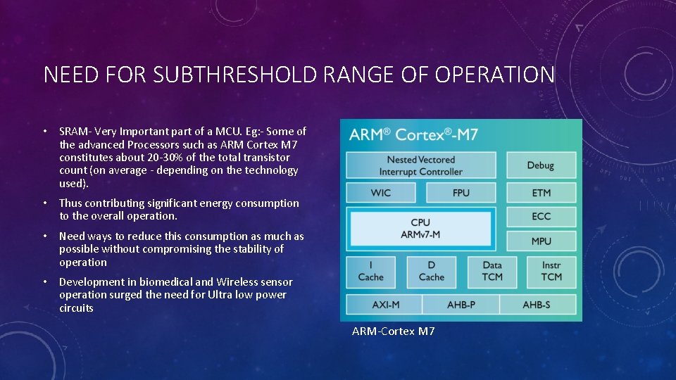
NEED FOR SUBTHRESHOLD RANGE OF OPERATION • SRAM- Very Important part of a MCU. Eg: - Some of the advanced Processors such as ARM Cortex M 7 constitutes about 20 -30% of the total transistor count (on average - depending on the technology used). • Thus contributing significant energy consumption to the overall operation. • Need ways to reduce this consumption as much as possible without compromising the stability of operation • Development in biomedical and Wireless sensor operation surged the need for Ultra low power circuits ARM-Cortex M 7
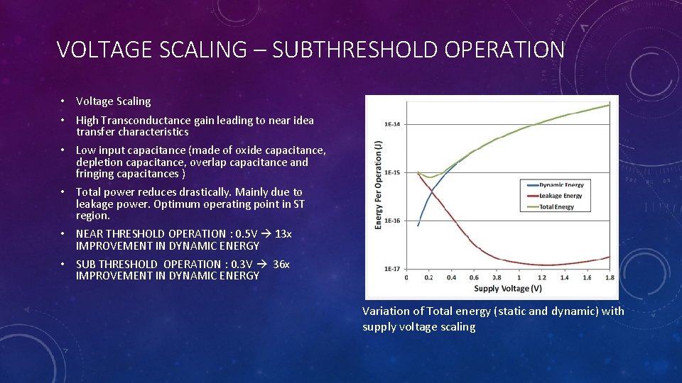
VOLTAGE SCALING – SUBTHRESHOLD OPERATION • Voltage Scaling • High Transconductance gain leading to near idea transfer characteristics • Low input capacitance (made of oxide capacitance, depletion capacitance, overlap capacitance and fringing capacitances ) • Total power reduces drastically. Mainly due to leakage power. Optimum operating point in ST region. • NEAR THRESHOLD OPERATION : 0. 5 V 13 x IMPROVEMENT IN DYNAMIC ENERGY • SUB THRESHOLD OPERATION : 0. 3 V 36 x IMPROVEMENT IN DYNAMIC ENERGY Variation of Total energy (static and dynamic) with supply voltage scaling
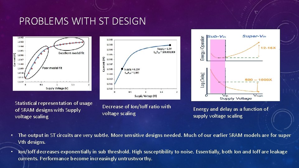
PROBLEMS WITH ST DESIGN Statistical representation of usage of SRAM designs with Supply voltage scaling Decrease of Ion/Ioff ratio with voltage scaling Energy and delay as a function of supply voltage scaling • The output in ST circuits are very subtle. More sensitive designs needed. Much of our earlier SRAM models are for super Vth designs. • Ion/Ioff decreases exponentially in sub threshold. High susceptibility to noise. Essentially, both Ion and Ioff are leakage currents. Performance become increasingly untrustworthy.

PHASE 1 : ACHIEVING STO MAIN COMPONENTS • • Ring oscillator 3 bit counter D flip flops for shifting 8: 1 MUX using transmission gates Varying reference _clock time period decides the sampling. This decides the value till which the counter can reach Sampling simultaneously achieves shifting the outputs to MUX
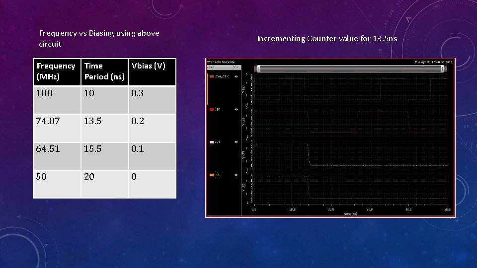
Frequency vs Biasing using above circuit Frequency Time Vbias (V) (MHz) Period (ns) 100 10 0. 3 74. 07 13. 5 0. 2 64. 51 15. 5 0. 1 50 20 0 Incrementing Counter value for 13. 5 ns

Operating Frequency Vs Bias voltage 0. 35 For 15. 5 ns 0. 3 Bias voltage (V) 0. 25 For 20 ns 0. 2 0. 15 0. 1 0. 05 0 0 20 40 60 Frequency (MHz) 80 100 120
PHASE 2: ANALYSIS OF ST-SRAM CIRCUITS • Compare the existing SRAM models with an Virtual Ground based PPN design. • The proposed design overcomes most of the design faults of the previous generation • Analysis is mainly based on N stability curves • Future works based on Monte. Carlo Simulations for all the discussed models • Analysis of how Leakage power varies for these models
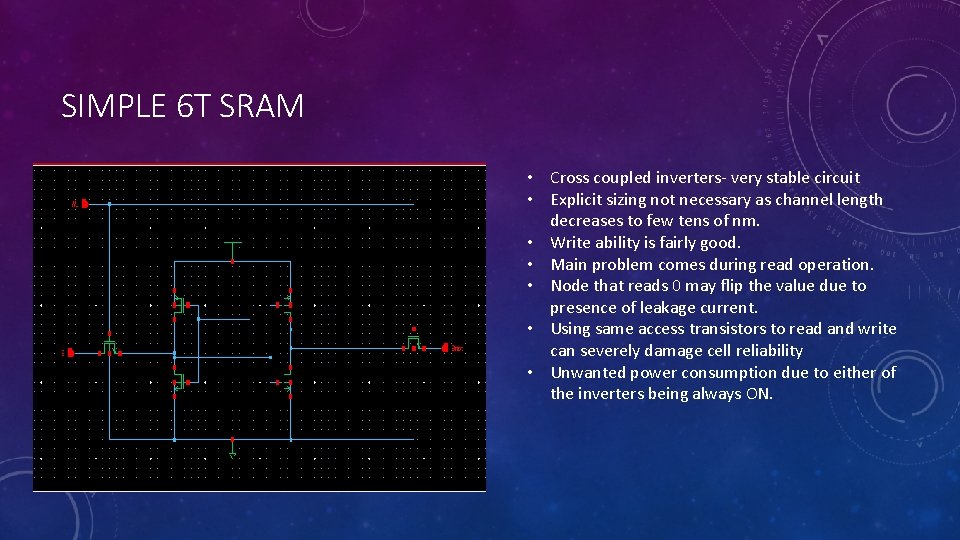
SIMPLE 6 T SRAM • Cross coupled inverters- very stable circuit • Explicit sizing not necessary as channel length decreases to few tens of nm. • Write ability is fairly good. • Main problem comes during read operation. • Node that reads 0 may flip the value due to presence of leakage current. • Using same access transistors to read and write can severely damage cell reliability • Unwanted power consumption due to either of the inverters being always ON.
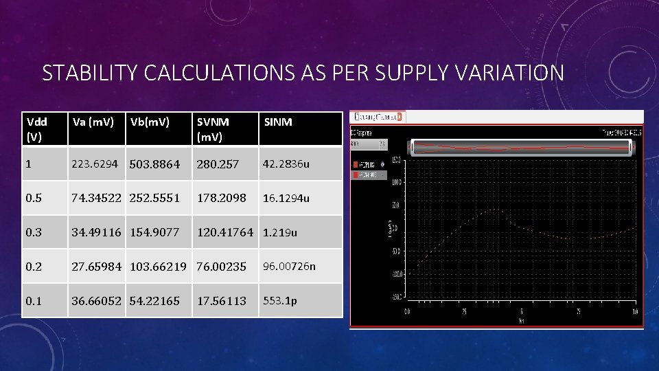
STABILITY CALCULATIONS AS PER SUPPLY VARIATION Vdd (V) Va (m. V) 1 Vb(m. V) SVNM (m. V) SINM 223. 6294 503. 8864 280. 257 42. 2836 u 0. 5 74. 34522 252. 5551 178. 2098 16. 1294 u 0. 3 34. 49116 154. 9077 120. 41764 1. 219 u 0. 2 27. 65984 103. 66219 76. 00235 96. 00726 n 0. 1 36. 66052 54. 22165 553. 1 p 17. 56113
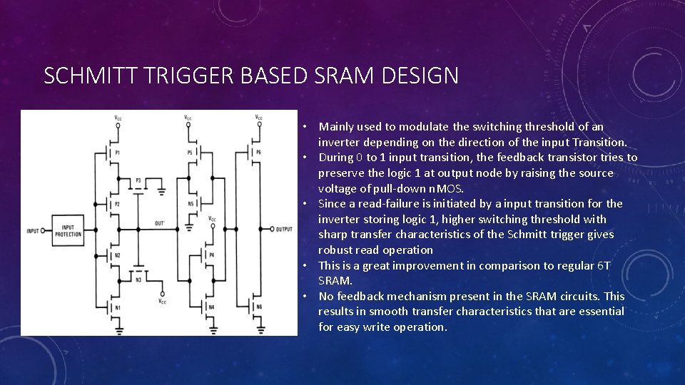
SCHMITT TRIGGER BASED SRAM DESIGN • Mainly used to modulate the switching threshold of an inverter depending on the direction of the input Transition. • During 0 to 1 input transition, the feedback transistor tries to preserve the logic 1 at output node by raising the source voltage of pull-down n. MOS. • Since a read-failure is initiated by a input transition for the inverter storing logic 1, higher switching threshold with sharp transfer characteristics of the Schmitt trigger gives robust read operation • This is a great improvement in comparison to regular 6 T SRAM. • No feedback mechanism present in the SRAM circuits. This results in smooth transfer characteristics that are essential for easy write operation.

SCHMITT TRIGGER BASED SRAM DESIGN Working essentially same as Schmitt trigger discussed above. • No upper feedback path to have a smooth write operation • During read operation, (if Vl stores 0 and Vr stores 1), if WL becomes 1, the node Vl has to be raised till the switching threshold to cause switching • Meanwhile, Vr is near Vdd because of AXR. This raises the switching needed to flip NR 1. Thus a strongly latched Vr does not allow Vl to raise because of this method. •
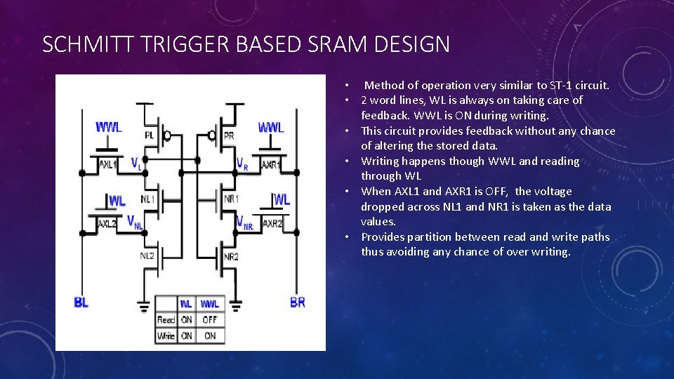
SCHMITT TRIGGER BASED SRAM DESIGN • Method of operation very similar to ST-1 circuit. • 2 word lines, WL is always on taking care of feedback. WWL is ON during writing. • This circuit provides feedback without any chance of altering the stored data. • Writing happens though WWL and reading through WL • When AXL 1 and AXR 1 is OFF, the voltage dropped across NL 1 and NR 1 is taken as the data values. • Provides partition between read and write paths thus avoiding any chance of over writing.

SCHMITT TRIGGER BASED SRAM DESIGN
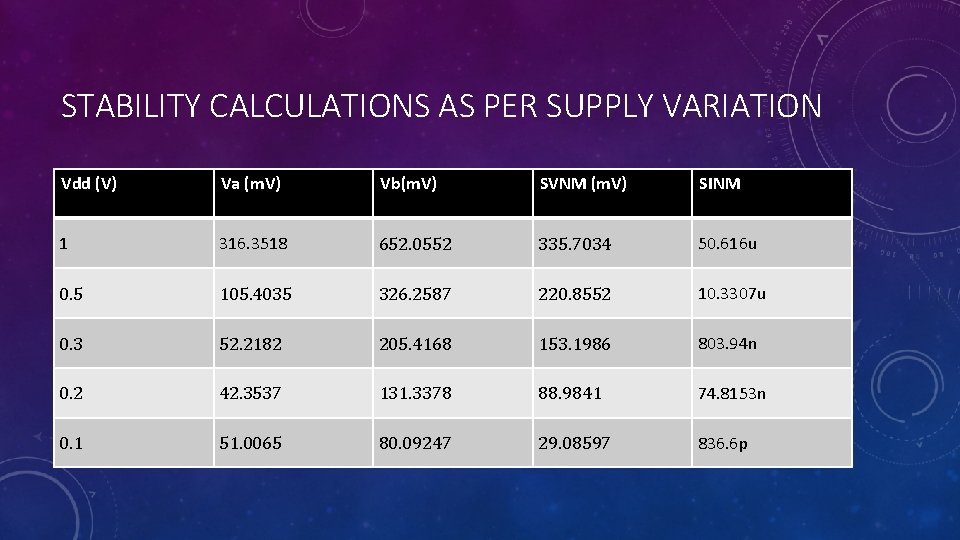
STABILITY CALCULATIONS AS PER SUPPLY VARIATION Vdd (V) Va (m. V) Vb(m. V) SVNM (m. V) SINM 1 316. 3518 652. 0552 335. 7034 50. 616 u 0. 5 105. 4035 326. 2587 220. 8552 10. 3307 u 0. 3 52. 2182 205. 4168 153. 1986 803. 94 n 0. 2 42. 3537 131. 3378 88. 9841 74. 8153 n 0. 1 51. 0065 80. 09247 29. 08597 836. 6 p
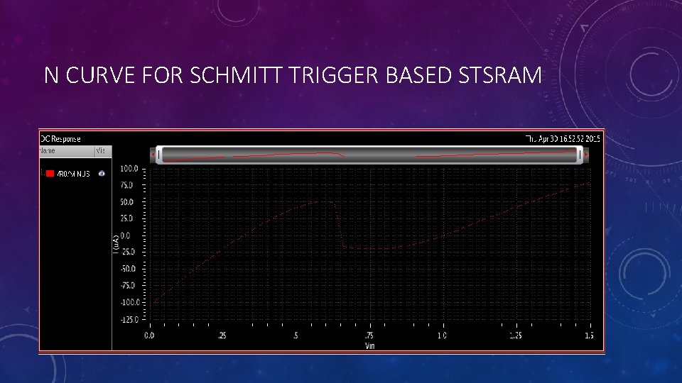
N CURVE FOR SCHMITT TRIGGER BASED STSRAM

VIRTUAL GROUND BASED PPN ST-SRAM DESIGN • Schmitt trigger based designs solve most of the read stability issues encountered in normal 6 T SRAM. • One inherent problem with the feedback mechanism is “transient voltage glitch”. • Occasional but costly in terms of stability • That is the node storing 0 when being read can at times flip to 1 if any transistors in the feedback path do not switch ON. • This design handles the above issue. • 2 PPN inverters. PQ and PQb are pseudo storage nodes whereas data is actually stored in Q and Qb • Separate discharge path for Pq and PQb with an access transistor and a NMOS. • VGND is connected to GND only during read. • Any transient glitch in the storage node is reflected in the pseudo storage nodes that discharge. • This reflects in the storage nodes as well.

VIRTUAL GROUND BASED PPN ST-SRAM DESIGN
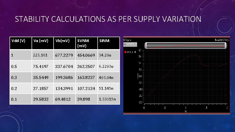
STABILITY CALCULATIONS AS PER SUPPLY VARIATION Vdd (V) Va (m. V) Vb(m. V) SVNM (m. V) 1 223. 161 677. 2279 454. 0669 34. 29 u 0. 5 75. 4197 337. 6704 262. 2507 6. 2293 u 0. 3 35. 5449 199. 3686 163. 8237 493. 94 n 0. 2 27. 1857 134. 3991 107. 2134 51. 145 n 0. 1 29. 5832 69. 4812 39. 898 SINM 1. 33015 n
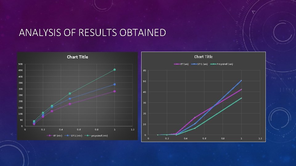
ANALYSIS OF RESULTS OBTAINED Chart Title 500 6 T (u. A) 450 ST-1 (u. A) Proposed (u. A) 60 400 50 300 40 250 200 30 150 20 100 50 0 10 0 0. 2 0. 4 6 T (m. V) 0. 6 ST-1 (m. V) 0. 8 proposed (m. V) 1 1. 2 0 0 0. 2 0. 4 0. 6 0. 8 1 1. 2
FUTURE WORK • Monte Carlo Simulations for all the ST SRAM types to understand how the Ion/Ioff ratio varies in each design • Performing Leakage calculations for all STSRAM designs and finding the optimum design based on leakage power THANK YOU

REFERENCES • Benton H. Calhoun, “Low energy Digital circuit Design Using Sub-threshold Operation”, Massachusetts Institute of Technology, 2005 • Jabulani Nyathi, Brent Bero and Ryan Mc. Kinlay, "A Tunable Body • Biasing Scheme for Ultra-Low Power and High Speed CMOS Designs" • in International Symposium on Low Power Electronics and Design - • 2006. October 4 -6, 2006 • Ashok Srivatsava and Chuang Zhang, "An Adaptive Body-Bias Generator for Low Voltage CMOS VLSI Circuits", International Journal of Distributed Sensor Networks, 4: 213– 222, 2008 • Neeta Pande, Rishi Pandel, Tanvi Mitta, Kirti Gupta, "Rajeshwari Pandey, Ring and Coupled Ring Oscillator in Subthreshold Region", Signal Propagation and Computer Technology (ICSPCT), 2014 International Conference, July 2014 • Roy, K. , Kulkarni, J. P. , Circuit Res. Lab. , Intel Corp. , Hillsboro, OR, USA, "Ultralow-Voltage Process-Variation-Tolerant Schmitt-Trigger-Based SRAM Design" Very Large Scale Integration (VLSI) Systems, IEEE Transactions on (Volume: 20 , Issue: 2 ), 2012 • J. P. Kulkarni, K. Kim and K. Roy, “A 160 m. V Robust • Schmitt Trigger based Subthreshold SRAM” IEEE Journal • of Solid State Circuits, vol. 42, no. 10, pp. 2303 -2313, October 2007 • J. P. Kulkarni, K. Kim and K. Roy, “Process Variation Tolerant SRAM Array for Ultra Low Voltage Applications” Design Automation Conference, 2008. DAC 2008. 45 th ACM/IEEE, October 2008 • Cheng-Hung Lo, Shi-Yu Huang "P-P-N Based 10 T SRAM Cell for Low-Leakage and Resilient Subthreshold Operation", IEEE JOURNAL OF SOLID-STATE CIRCUITS, VOL. 46, NO. 3, MARCH 2011 • Evelyn Grossar, Michele Stucchi, Karen Maex, Wim Dehaene, "Read Stability and Write-Ability Analysis of SRAM Cells for Nanometer Technologies"IEEE JOURNAL OF SOLID-STATE CIRCUITS, VOL. 41, NO. 11, NOVEMBER 2006
- Slides: 23