Stability 1 TI Precision Labs Op Amps Developed

Stability – 1 TI Precision Labs – Op Amps Developed by Collin Wells, Art Kay, and Ian Williams 1
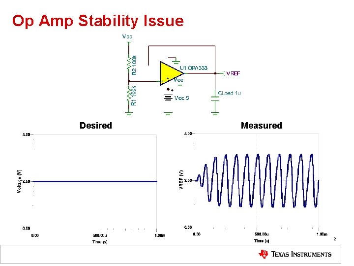
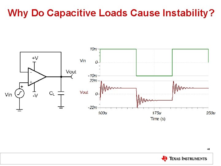
Op Amp Stability Issue Desired Measured 2
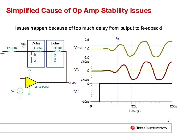
Simplified Cause of Op Amp Stability Issues 30 p Issues happen because of too much delay from output to feedback! 3
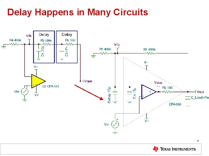
30 p Delay Happens in Many Circuits 4
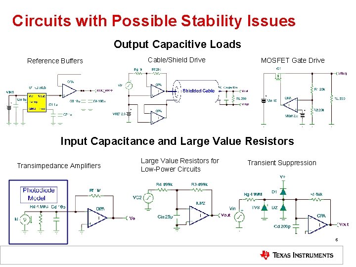
Circuits with Possible Stability Issues Output Capacitive Loads Reference Buffers Cable/Shield Drive MOSFET Gate Drive Input Capacitance and Large Value Resistors Transimpedance Amplifiers Large Value Resistors for Low-Power Circuits Transient Suppression 5
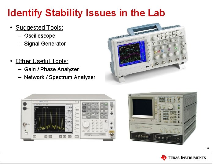
Identify Stability Issues in the Lab • Suggested Tools: – Oscilloscope – Signal Generator • Other Useful Tools: – Gain / Phase Analyzer – Network / Spectrum Analyzer 6
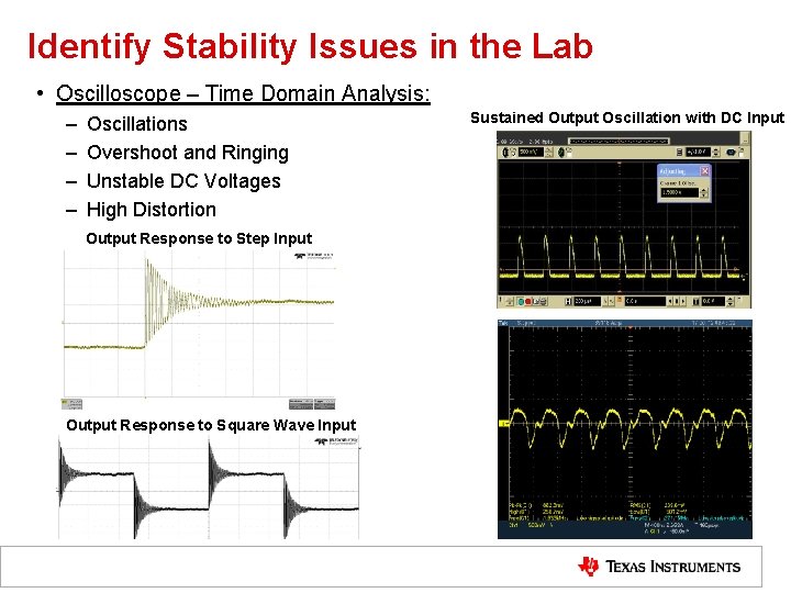
Identify Stability Issues in the Lab • Oscilloscope – Time Domain Analysis: – – Oscillations Overshoot and Ringing Unstable DC Voltages High Distortion Sustained Output Oscillation with DC Input Output Response to Step Input Output Response to Square Wave Input 7
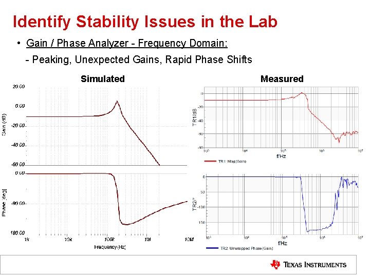
Identify Stability Issues in the Lab • Gain / Phase Analyzer - Frequency Domain: - Peaking, Unexpected Gains, Rapid Phase Shifts Simulated Measured 8
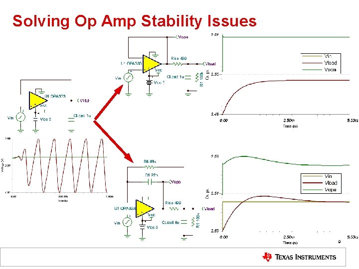
Solving Op Amp Stability Issues Riso 499 9
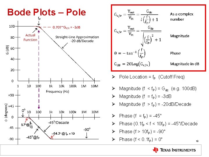
Bode Plots – Pole Ø Pole Location = f. P (Cutoff Freq) Ø Magnitude (f < f. P) = Gdc (e. g. 100 d. B) Ø Magnitude (f = f. P) = -3 d. B Ø Magnitude (f > f. P) = -20 d. B/Decade Ø Phase (f = f. P) = -45° Ø Phase (0. 1 f. P < f < 10 f. P) = -45°/Decade Ø Phase (f > 10 f. P) = -90° Ø Phase (f < 0. 1 f. P) = 0° 10
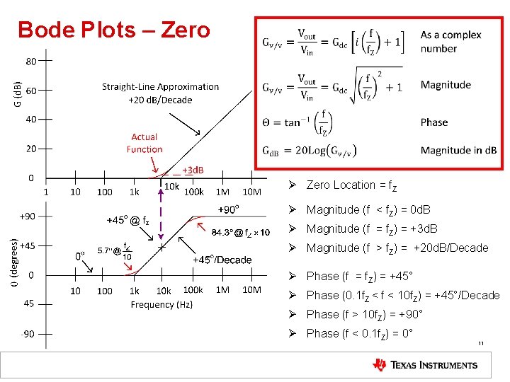
Bode Plots – Zero Ø Zero Location = f. Z Ø Magnitude (f < f. Z) = 0 d. B Ø Magnitude (f = f. Z) = +3 d. B Ø Magnitude (f > f. Z) = +20 d. B/Decade Ø Phase (f = f. Z) = +45° Ø Phase (0. 1 f. Z < f < 10 f. Z) = +45°/Decade Ø Phase (f > 10 f. Z) = +90° Ø Phase (f < 0. 1 f. Z) = 0° 11
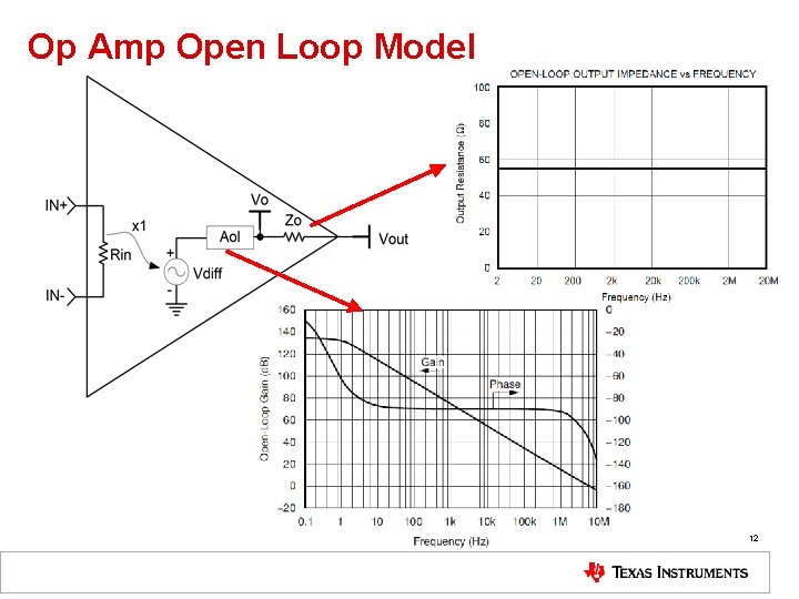
Op Amp Open Loop Model 12
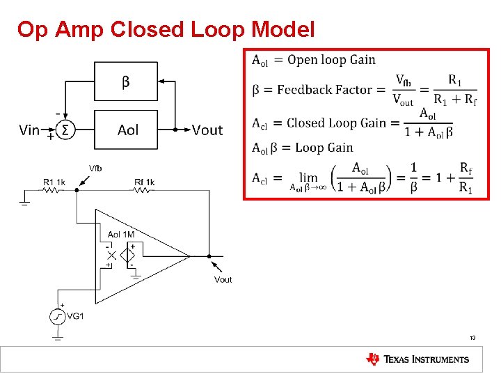
Op Amp Closed Loop Model 13
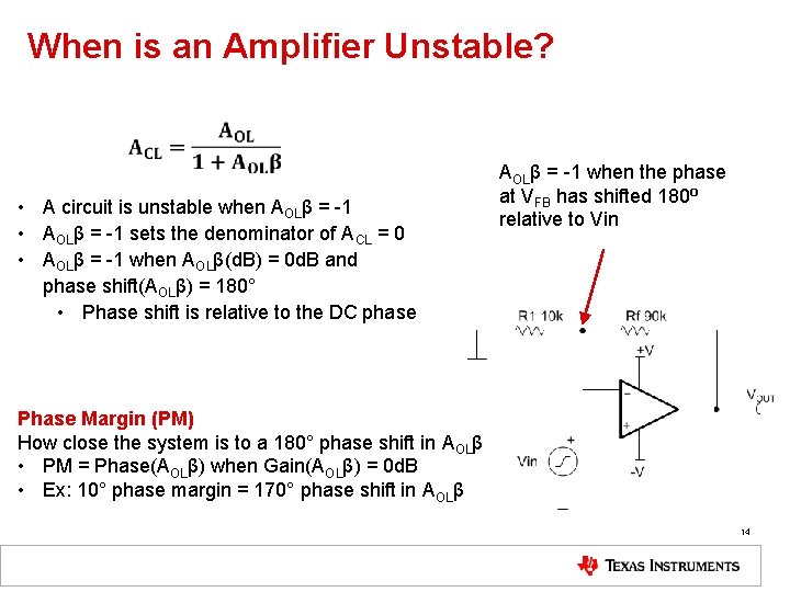
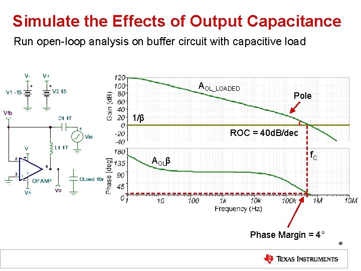
When is an Amplifier Unstable? • A circuit is unstable when AOLβ = -1 • AOLβ = -1 sets the denominator of ACL = 0 • AOLβ = -1 when AOLβ(d. B) = 0 d. B and phase shift(AOLβ) = 180° • Phase shift is relative to the DC phase AOLβ = -1 when the phase at VFB has shifted 180⁰ relative to Vin Phase Margin (PM) How close the system is to a 180° phase shift in AOLβ • PM = Phase(AOLβ) when Gain(AOLβ) = 0 d. B • Ex: 10° phase margin = 170° phase shift in AOLβ 14
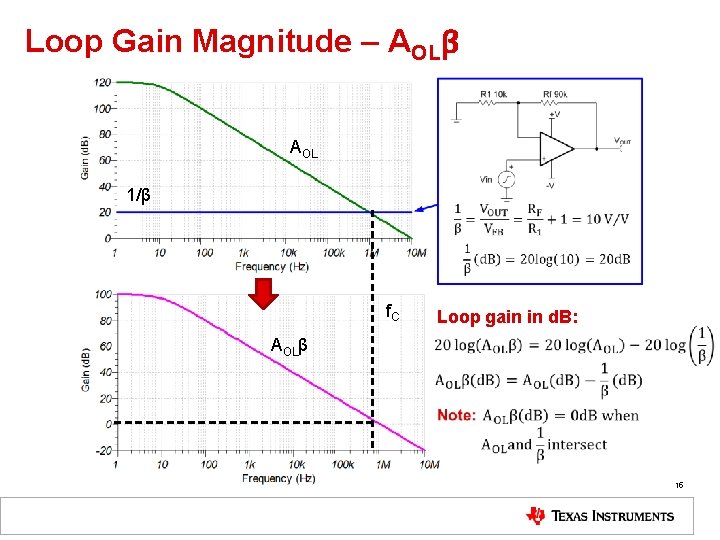
Loop Gain Magnitude – AOLβ AOL 1/β f. C AOLβ Loop gain in d. B: 15
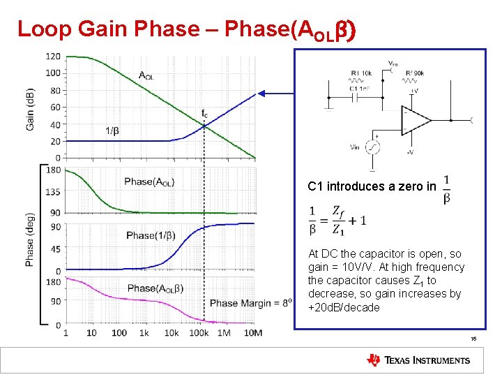
Loop Gain Phase – Phase(AOLβ) C 1 introduces a zero in At DC the capacitor is open, so gain = 10 V/V. At high frequency the capacitor causes Z 1 to decrease, so gain increases by +20 d. B/decade 16
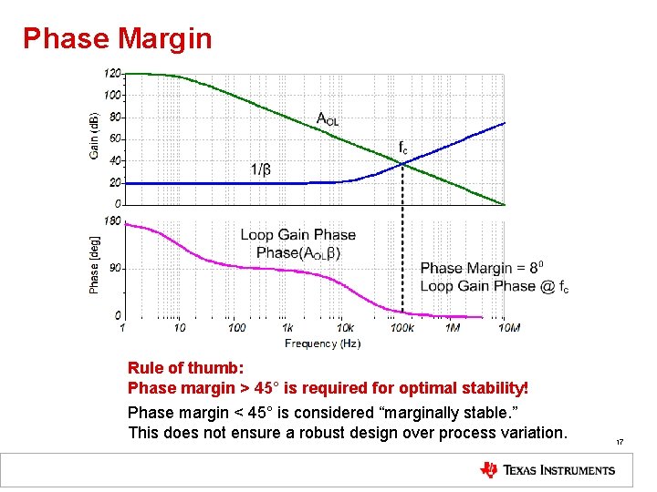
Phase Margin Rule of thumb: Phase margin > 45° is required for optimal stability! Phase margin < 45° is considered “marginally stable. ” This does not ensure a robust design over process variation. 17
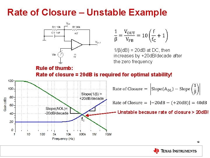
Rate of Closure – Unstable Example 1/β(d. B) = 20 d. B at DC, then increases by +20 d. B/decade after the zero frequency Rule of thumb: Rate of closure = 20 d. B is required for optimal stability! Unstable because rate of closure > 20 d. B! 18
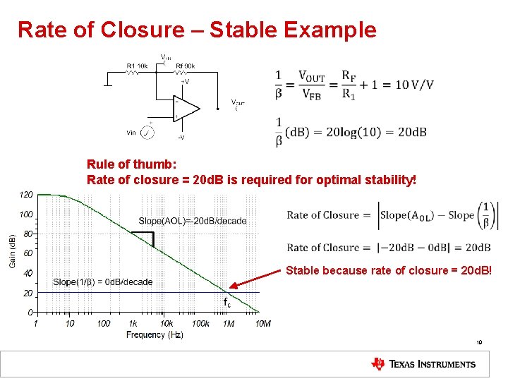
Rate of Closure – Stable Example Rule of thumb: Rate of closure = 20 d. B is required for optimal stability! Stable because rate of closure = 20 d. B! 19
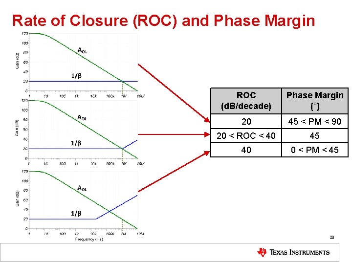
Rate of Closure (ROC) and Phase Margin ROC (d. B/decade) Phase Margin (°) 20 45 < PM < 90 20 < ROC < 40 45 40 0 < PM < 45 20
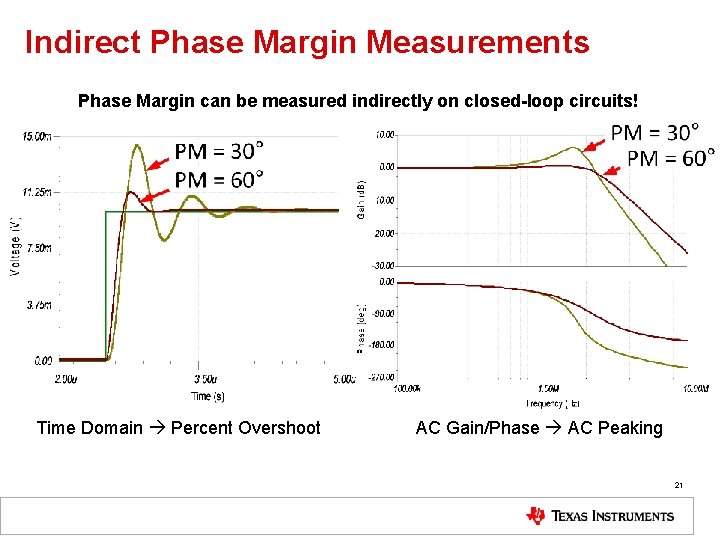
Indirect Phase Margin Measurements Phase Margin can be measured indirectly on closed-loop circuits! Time Domain Percent Overshoot AC Gain/Phase AC Peaking 21
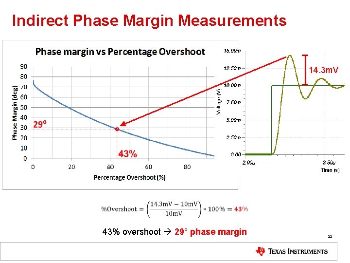
Indirect Phase Margin Measurements 14. 3 m. V 43% overshoot 29° phase margin 22
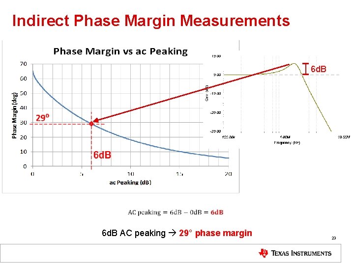
Indirect Phase Margin Measurements 6 d. B AC peaking 29° phase margin 23
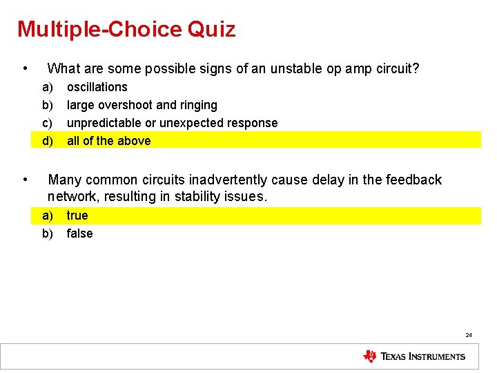
Multiple-Choice Quiz • What are some possible signs of an unstable op amp circuit? a) b) c) d) • oscillations large overshoot and ringing unpredictable or unexpected response all of the above Many common circuits inadvertently cause delay in the feedback network, resulting in stability issues. a) b) true false 24
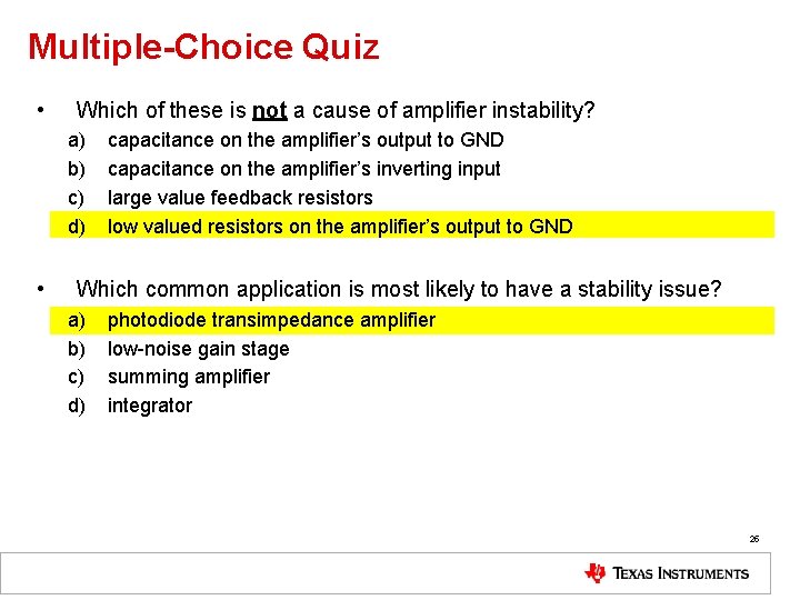
Multiple-Choice Quiz • Which of these is not a cause of amplifier instability? a) b) c) d) • capacitance on the amplifier’s output to GND capacitance on the amplifier’s inverting input large value feedback resistors low valued resistors on the amplifier’s output to GND Which common application is most likely to have a stability issue? a) b) c) d) photodiode transimpedance amplifier low-noise gain stage summing amplifier integrator 25
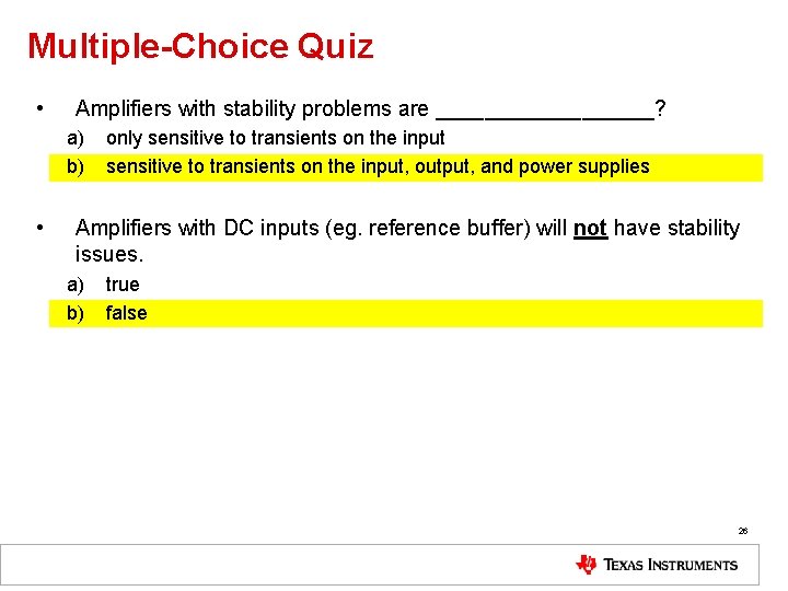
Multiple-Choice Quiz • Amplifiers with stability problems are _________? a) b) • only sensitive to transients on the input, output, and power supplies Amplifiers with DC inputs (eg. reference buffer) will not have stability issues. a) b) true false 26
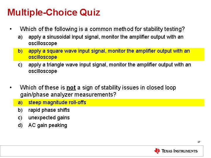
Multiple-Choice Quiz • Which of the following is a common method for stability testing? a) b) c) • apply a sinusoidal input signal, monitor the amplifier output with an oscilloscope apply a square wave input signal, monitor the amplifier output with an oscilloscope apply a triangle wave input signal, monitor the amplifier output with an oscilloscope Which of these is not a sign of stability issues in closed loop gain/phase analyzer measurements? a) b) c) d) steep magnitude roll-offs rapid phase shifts unexpected gains AC gain peaking 27
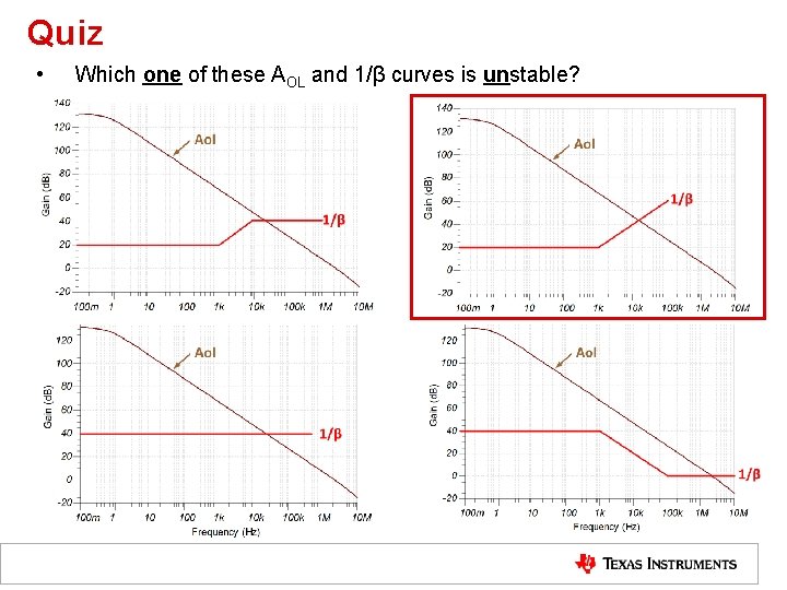
Quiz • Which one of these AOL and 1/β curves is unstable?
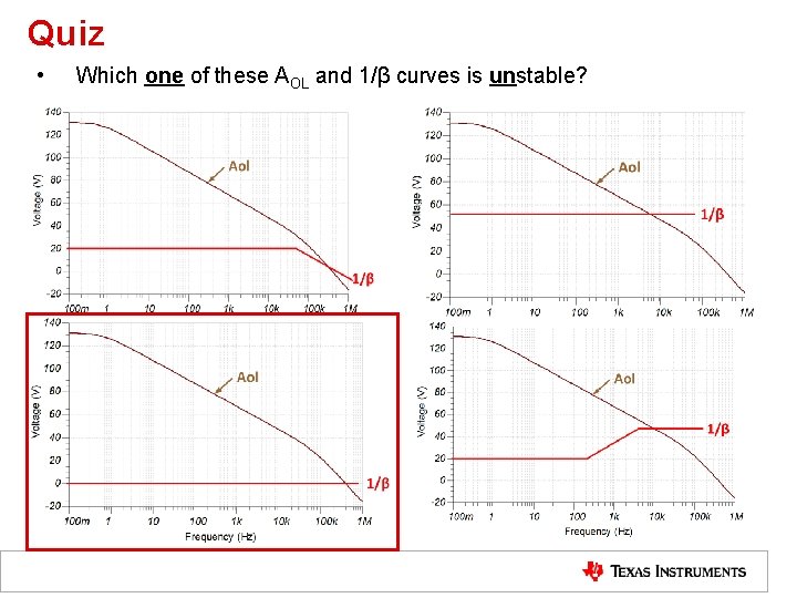
Quiz • Which one of these AOL and 1/β curves is unstable?
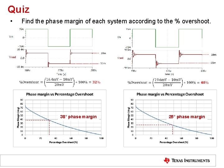
Quiz • Find the phase margin of each system according to the % overshoot. 38° phase margin 25° phase margin
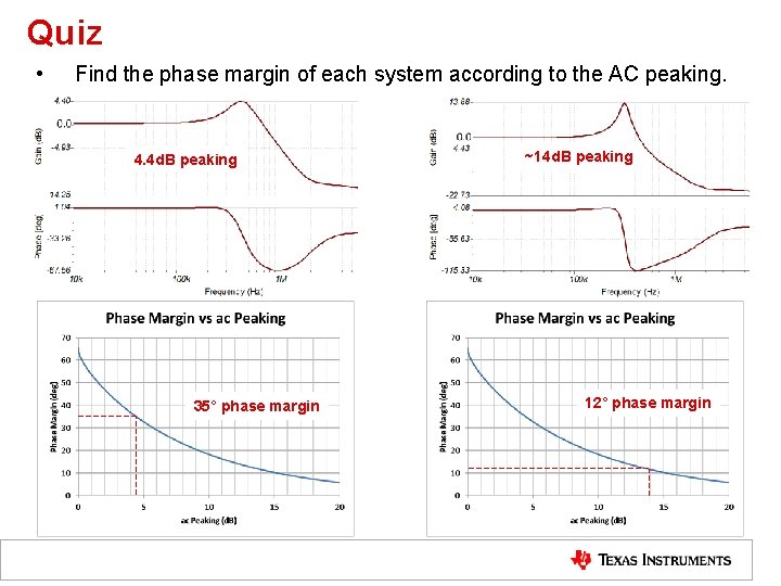
Quiz • Find the phase margin of each system according to the AC peaking. 4. 4 d. B peaking 35° phase margin ~14 d. B peaking 12° phase margin 31
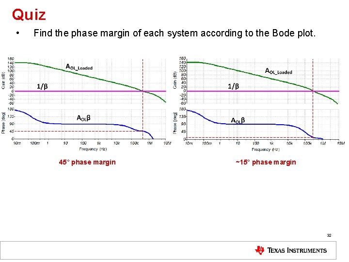
Quiz • Find the phase margin of each system according to the Bode plot. 45° phase margin ~15° phase margin 32

Stability – 2 TI Precision Labs – Op Amps Developed by Collin Wells, Art Kay, and Ian Williams 33
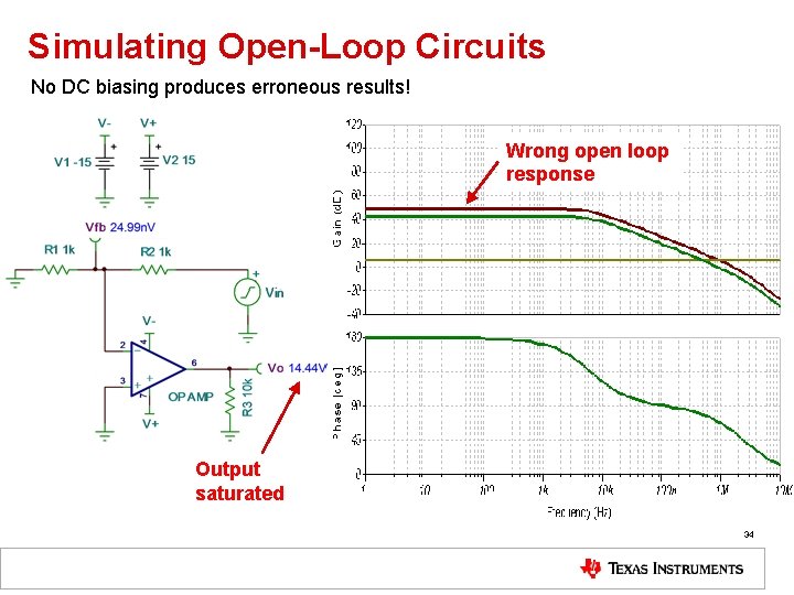
Simulating Open-Loop Circuits No DC biasing produces erroneous results! Wrong open loop response Output saturated 34
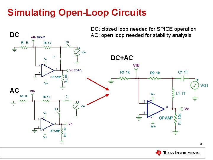
Simulating Open-Loop Circuits DC: closed loop needed for SPICE operation AC: open loop needed for stability analysis DC RL DC+AC RL RL AC 35
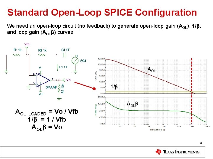
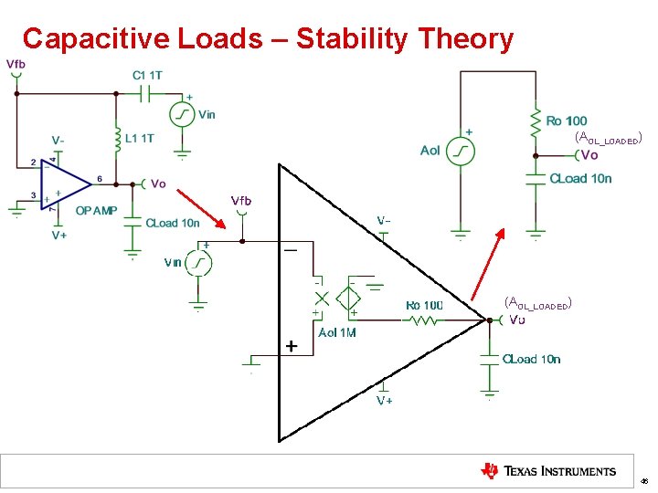
Standard Open-Loop SPICE Configuration We need an open-loop circuit (no feedback) to generate open-loop gain (AOL), 1/β, and loop gain (AOLβ) curves AOL 1/β AOL_LOADED = Vo / Vfb 1/β = 1 / Vfb AOLβ = Vo 36
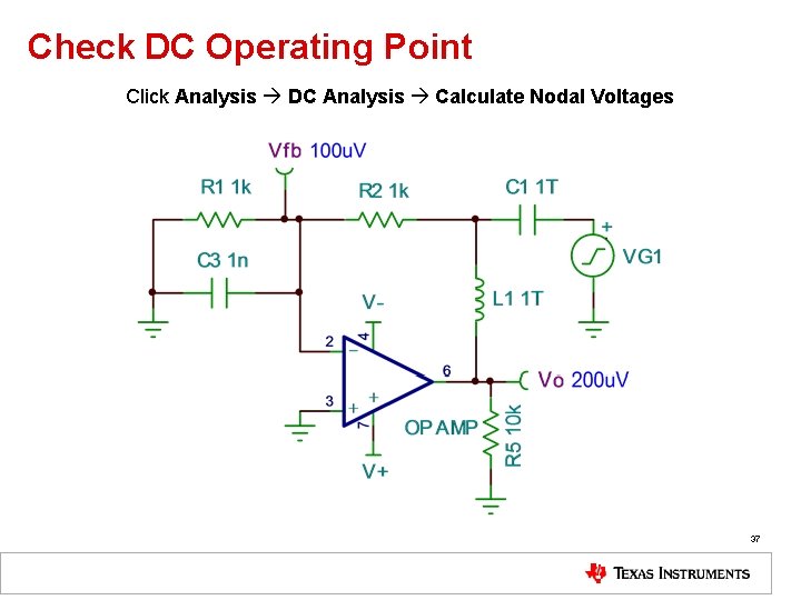
Check DC Operating Point Click Analysis DC Analysis Calculate Nodal Voltages 37
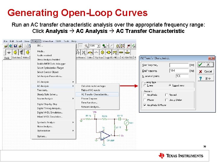
Generating Open-Loop Curves Run an AC transfer characteristic analysis over the appropriate frequency range: Click Analysis AC Transfer Characteristic 38
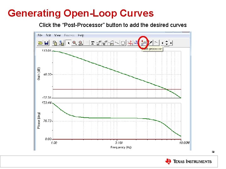
Generating Open-Loop Curves Click the “Post-Processor” button to add the desired curves 39

Generating Open-Loop Curves Perform math on the existing curves to create the new curves: AOL = Vo / Vfb 1/β = 1/Vfb AOLβ = Vo 40
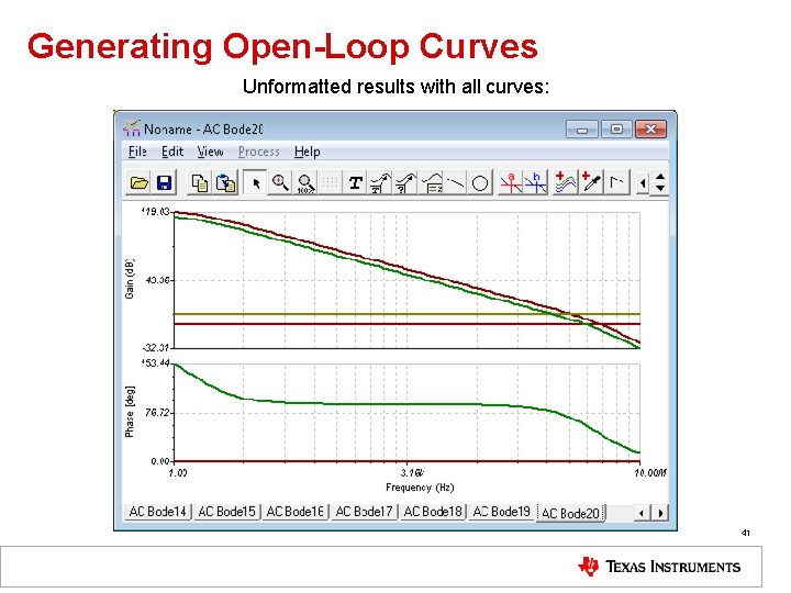
Generating Open-Loop Curves Unformatted results with all curves: 41
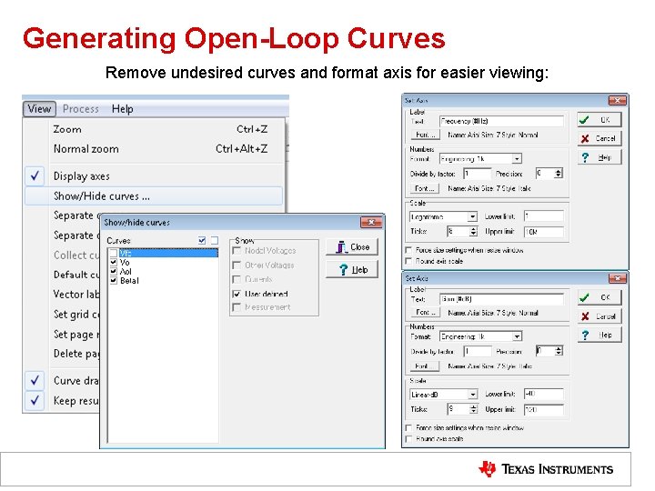
Generating Open-Loop Curves Remove undesired curves and format axis for easier viewing: 42
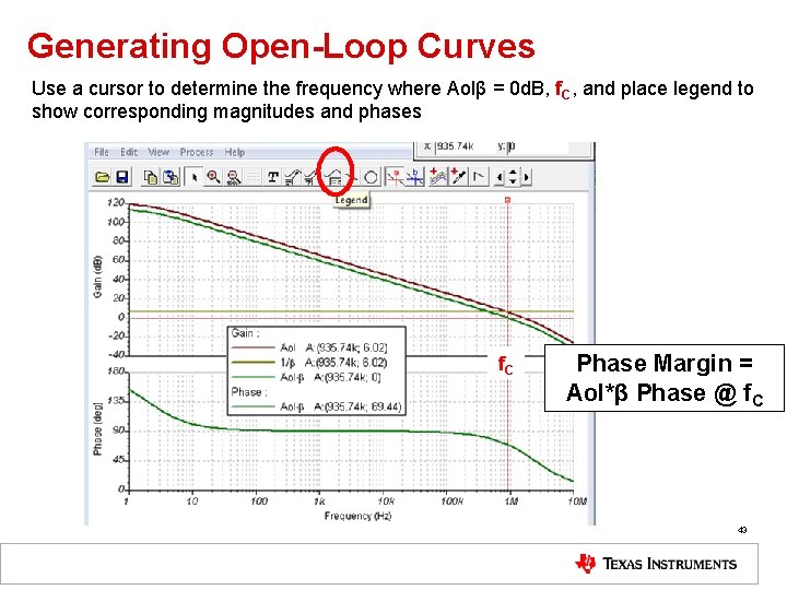
Generating Open-Loop Curves Use a cursor to determine the frequency where Aolβ = 0 d. B, f. C, and place legend to show corresponding magnitudes and phases f. C Phase Margin = Aol*β Phase @ f. C 43
Why Do Capacitive Loads Cause Instability? 44
Simulate the Effects of Output Capacitance Run open-loop analysis on buffer circuit with capacitive load AOL_LOADED Pole 1/β ROC = 40 d. B/dec AOLβ f. C Phase Margin = 4° 45
Capacitive Loads – Stability Theory (AOL_LOADED) 46
Capacitive Loads – Stability Theory Transfer Function: Pole Equation: 47
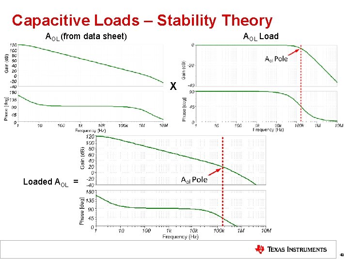
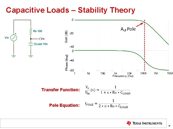
Capacitive Loads – Stability Theory AOL (from data sheet) AOL Load X Loaded AOL = 48
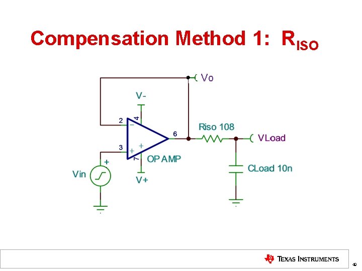
Compensation Method 1: RISO Vo 49
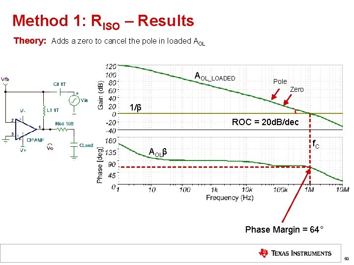
Method 1: RISO – Results Theory: Adds a zero to cancel the pole in loaded AOL_LOADED Pole Zero 1/β ROC = 20 d. B/dec AOLβ f. C Phase Margin = 64° 50
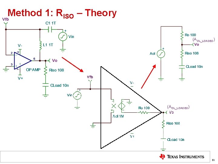
Method 1: RISO – Theory (AOL_LOADED) 51
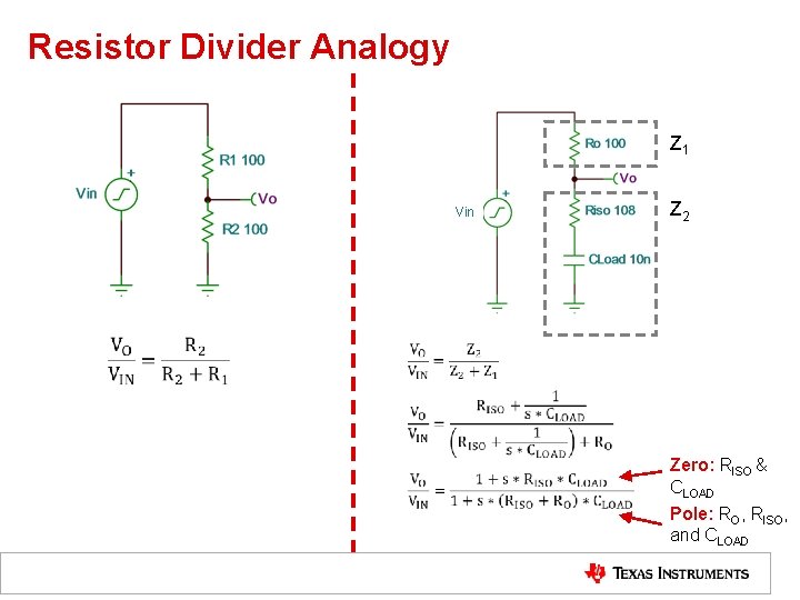
Resistor Divider Analogy Z 1 Vin Z 2 Zero: RISO & CLOAD Pole: RO, RISO, and CLOAD 52
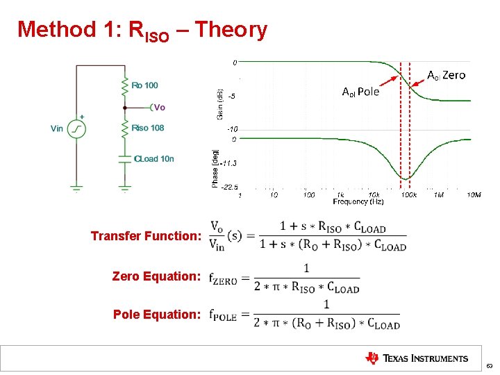
Method 1: RISO – Theory Transfer Function: Zero Equation: Pole Equation: 53
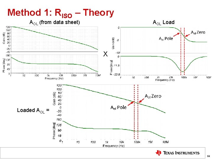
Method 1: RISO – Theory AOL (from data sheet) AOL Load X Loaded AOL = 54
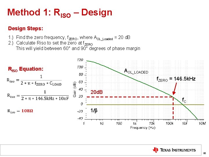
Method 1: RISO – Design Steps: 1. ) Find the zero frequency, f. ZERO, where AOL_Loaded = 20 d. B 2. ) Calculate Riso to set the zero at f. ZERO This will yield between 60° and 90° degrees of phase margin RISO Equation: AOL_LOADED f. ZERO = 146. 5 k. Hz 20 d. B f. C 1/β 55
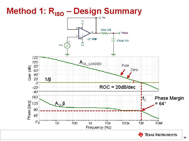
Method 1: RISO – Design Summary AOL_LOADED Pole Zero 1/β ROC = 20 d. B/dec AOLβ f. C Phase Margin = 64° 56
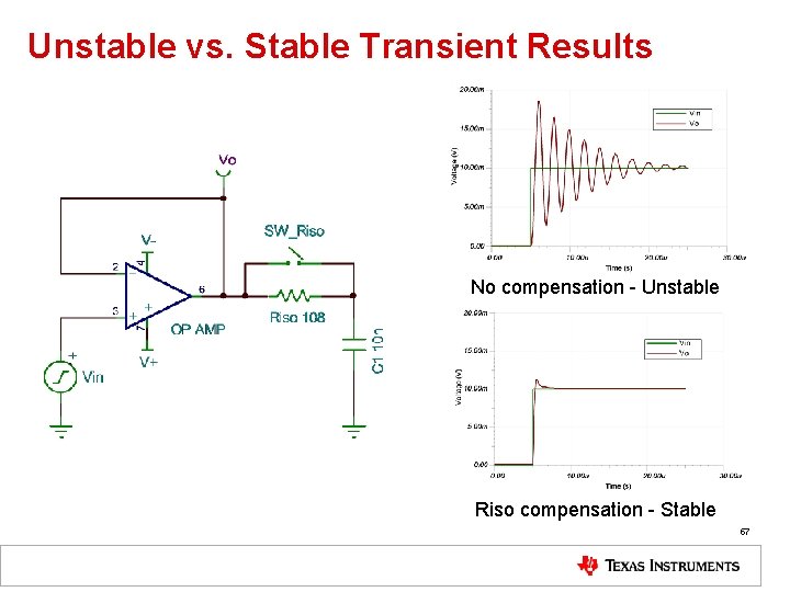
Unstable vs. Stable Transient Results No compensation - Unstable Riso compensation - Stable 57
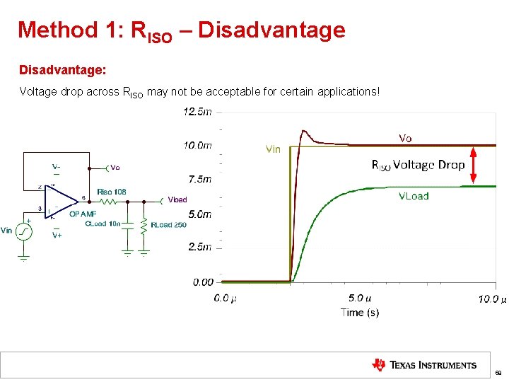
Method 1: RISO – Disadvantage: Voltage drop across RISO may not be acceptable for certain applications! 58
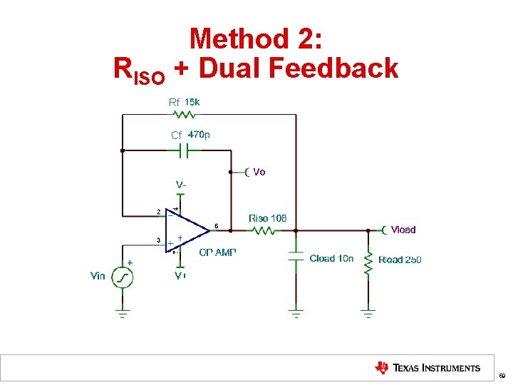
Method 2: RISO + Dual Feedback Rf Cf 59
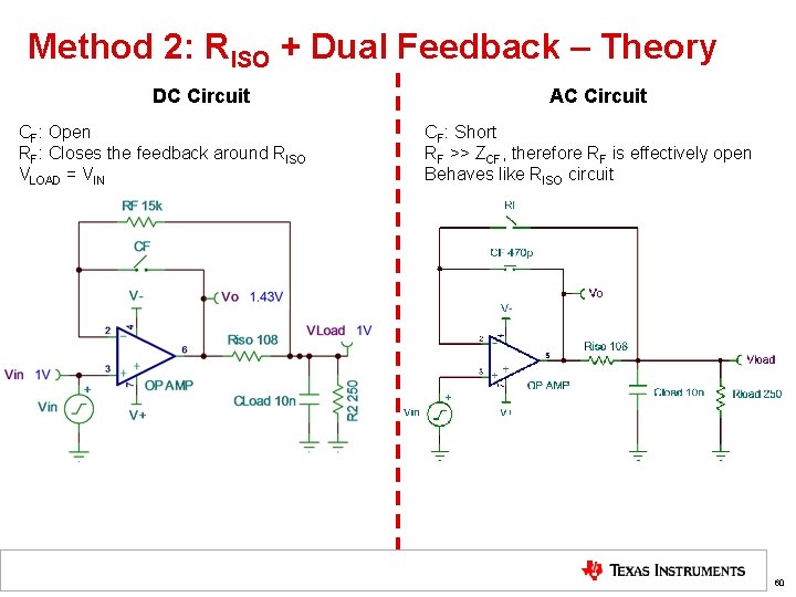
Method 2: RISO + Dual Feedback – Theory DC Circuit CF: Open RF: Closes the feedback around RISO VLOAD = VIN AC Circuit CF: Short RF >> ZCF, therefore RF is effectively open Behaves like RISO circuit 60
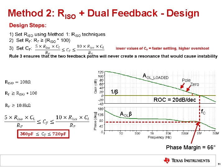
Method 2: RISO + Dual Feedback - Design AOL_LOADED Pole Zero 1/β ROC = 20 d. B/dec AOLβ f. C Phase Margin = 66° 61
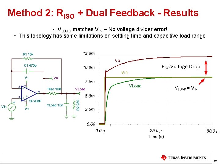
Method 2: RISO + Dual Feedback - Results • VLOAD matches VIN – No voltage divider error! • This topology has some limitations on settling time and capacitive load range 62
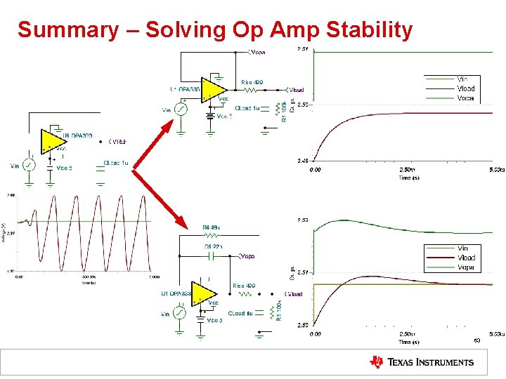
Summary – Solving Op Amp Stability Riso 499 63

Thanks for your time! 64
- Slides: 64