SRAM Mohammad Sharifkhani Effect of Mismatch Data Retention

- Slides: 52

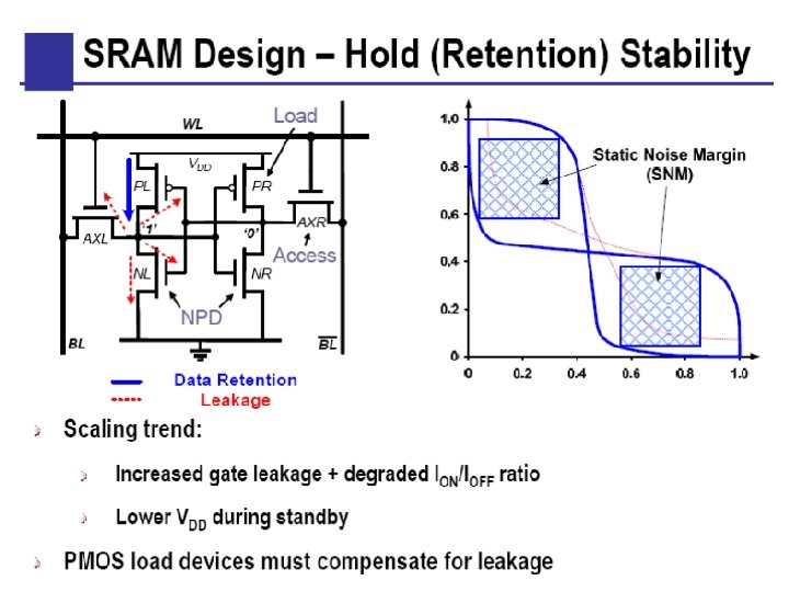
SRAM Mohammad Sharifkhani


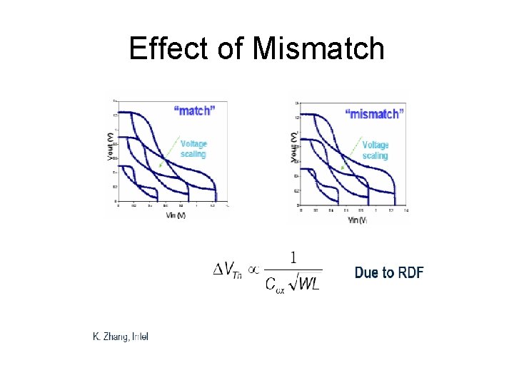
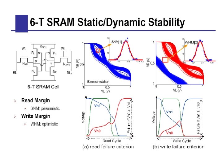
Effect of Mismatch

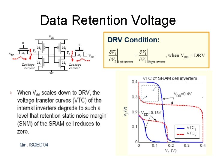
Data Retention Voltage

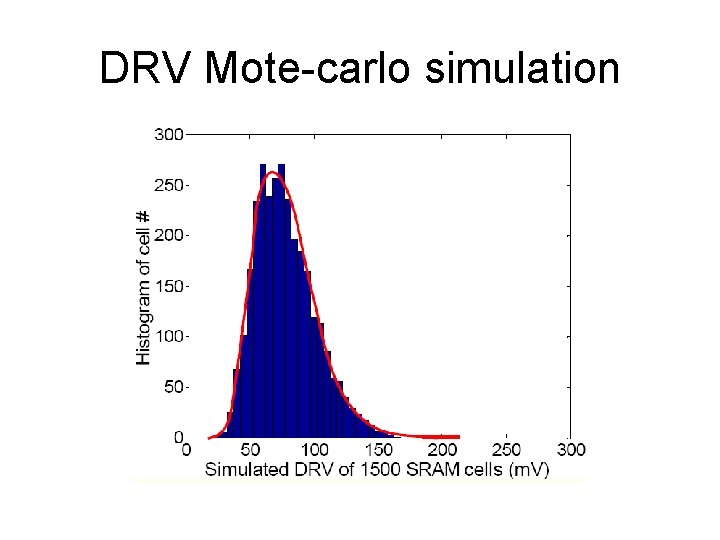
DRV Mote-carlo simulation


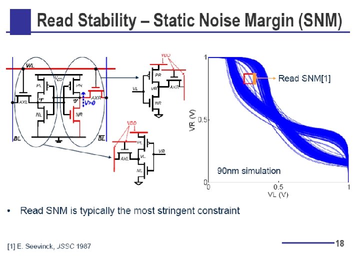
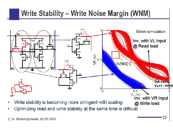
Inv. with VL Input @ Read load Init cond. VL=1, VH=0 Inv. with VR Input @ Write load

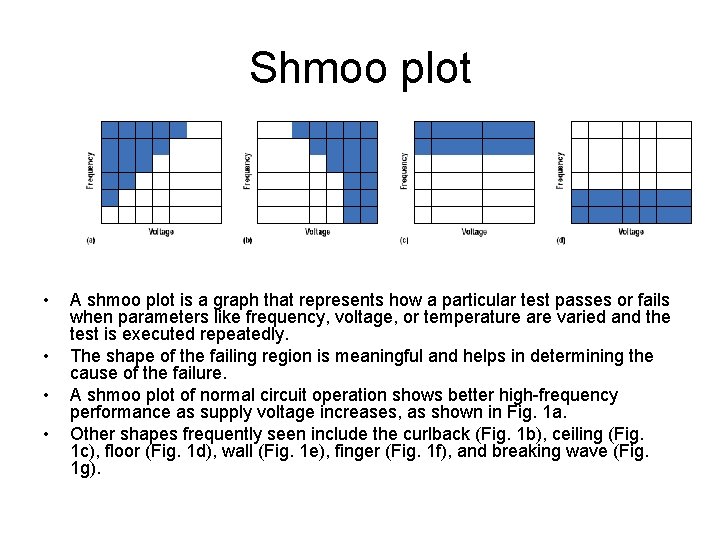
Shmoo plot • • A shmoo plot is a graph that represents how a particular test passes or fails when parameters like frequency, voltage, or temperature are varied and the test is executed repeatedly. The shape of the failing region is meaningful and helps in determining the cause of the failure. A shmoo plot of normal circuit operation shows better high-frequency performance as supply voltage increases, as shown in Fig. 1 a. Other shapes frequently seen include the curlback (Fig. 1 b), ceiling (Fig. 1 c), floor (Fig. 1 d), wall (Fig. 1 e), finger (Fig. 1 f), and breaking wave (Fig. 1 g).


Techniques for improving reliability • Read assist circuits • Write assist circuits • Error correction methods

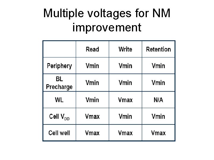
Multiple voltages for NM improvement

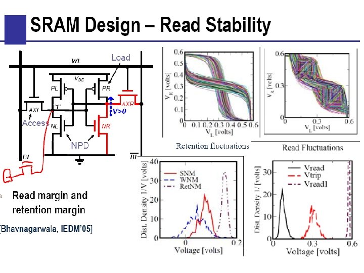
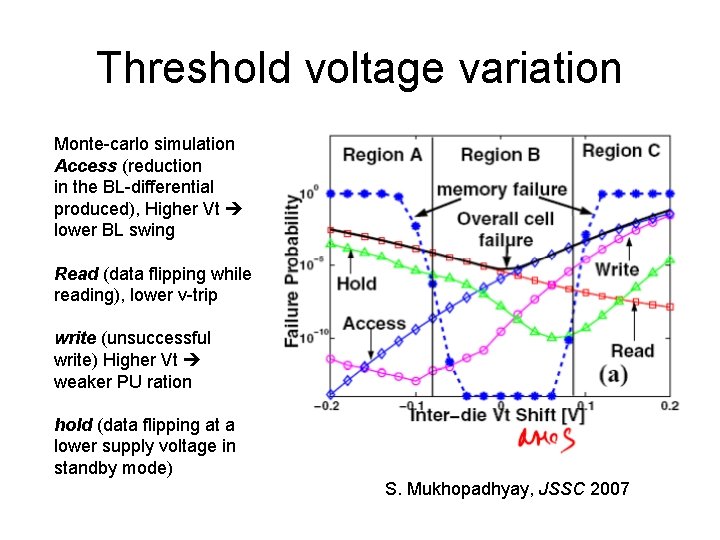
Threshold voltage variation Monte-carlo simulation Access (reduction in the BL-differential produced), Higher Vt lower BL swing Read (data flipping while reading), lower v-trip write (unsuccessful write) Higher Vt weaker PU ration hold (data flipping at a lower supply voltage in standby mode) S. Mukhopadhyay, JSSC 2007

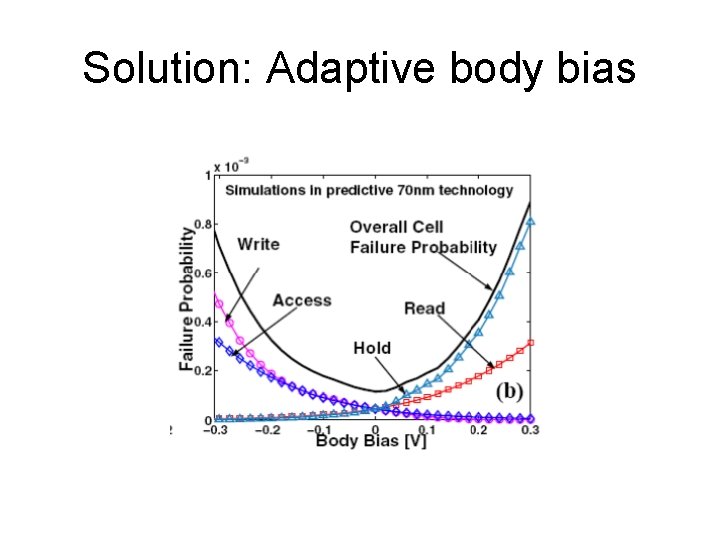
Solution: Adaptive body bias

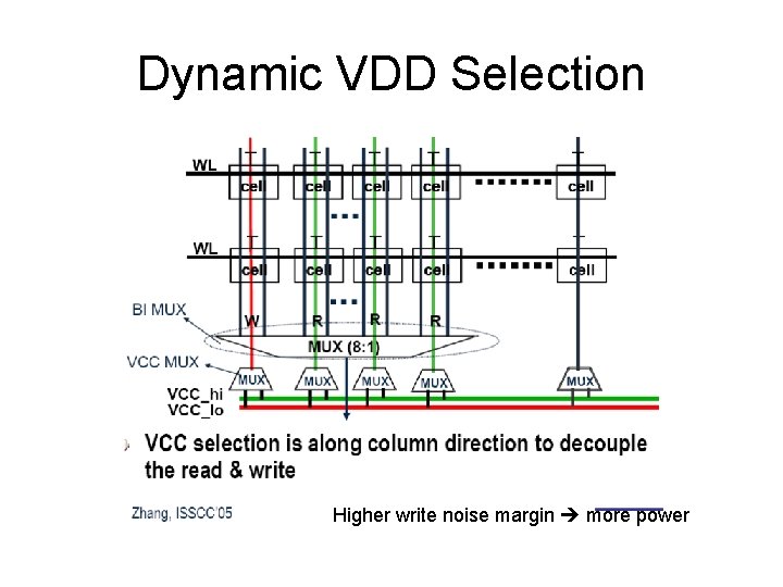
Dynamic VDD Selection Higher write noise margin more power

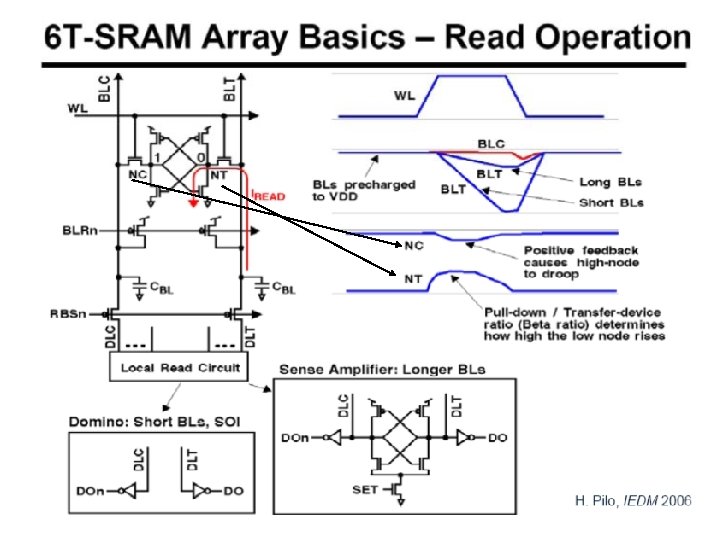
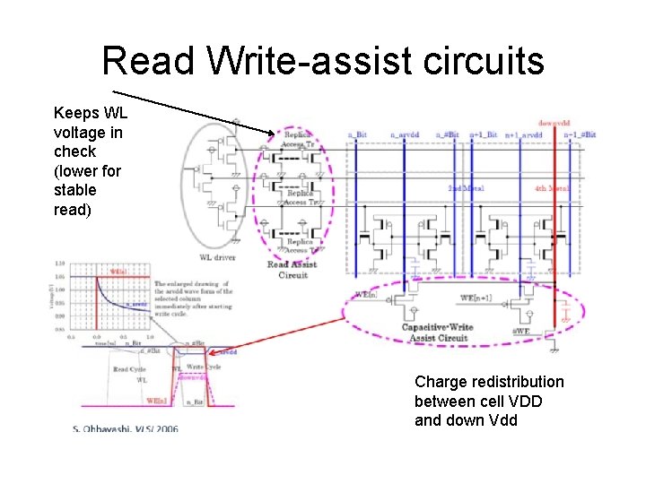
Read Write-assist circuits Keeps WL voltage in check (lower for stable read) Charge redistribution between cell VDD and down Vdd

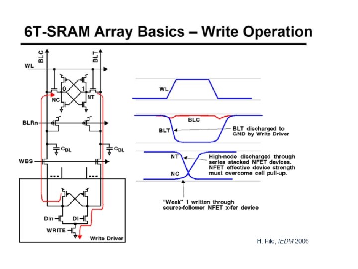
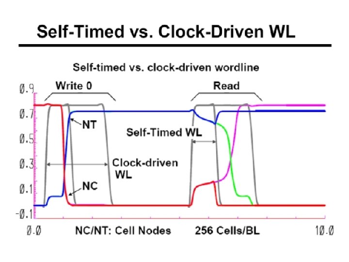
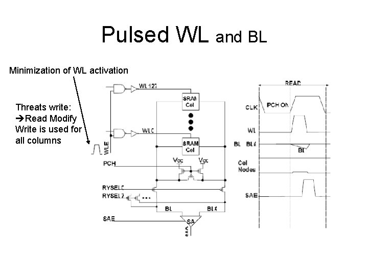
Pulsed WL and BL Minimization of WL activation Threats write: Read Modify Write is used for all columns

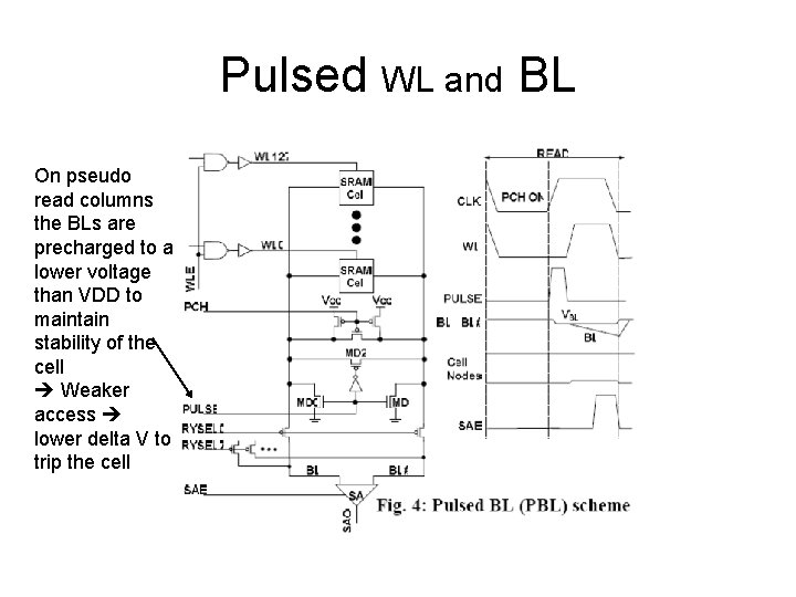
Pulsed WL and BL On pseudo read columns the BLs are precharged to a lower voltage than VDD to maintain stability of the cell Weaker access lower delta V to trip the cell

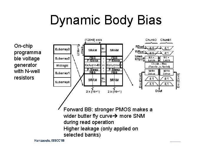
Dynamic Body Bias On-chip programma ble voltage generator with N-well resistors Forward BB: stronger PMOS makes a wider butter fly curve more SNM during read operation Higher leakage (only applied on selected banks)

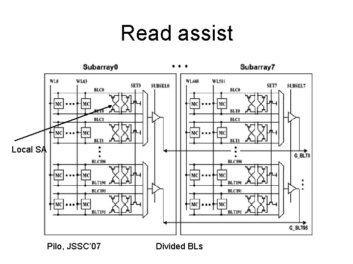
Read assist Local SA Pilo, JSSC’ 07 Divided BLs

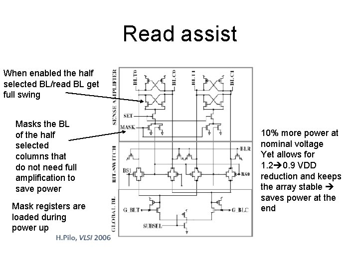
Read assist When enabled the half selected BL/read BL get full swing Masks the BL of the half selected columns that do not need full amplification to save power Mask registers are loaded during power up 10% more power at nominal voltage Yet allows for 1. 2 0. 9 VDD reduction and keeps the array stable saves power at the end

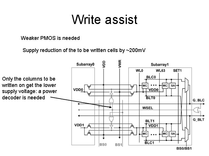
Write assist Weaker PMOS is needed Supply reduction of the to be written cells by ~200 m. V Only the columns to be written on get the lower supply voltage: a power decoder is needed

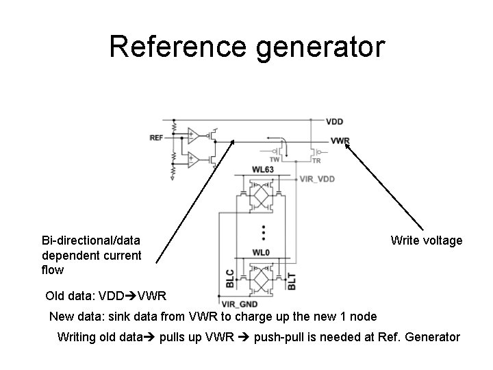
Reference generator Bi-directional/data dependent current flow Write voltage Old data: VDD VWR New data: sink data from VWR to charge up the new 1 node Writing old data pulls up VWR push-pull is needed at Ref. Generator

Redundancy in SRAMs

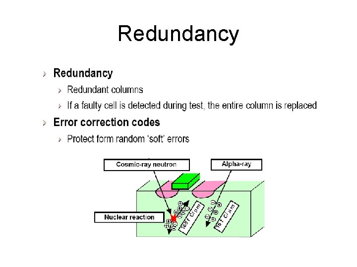
Redundancy

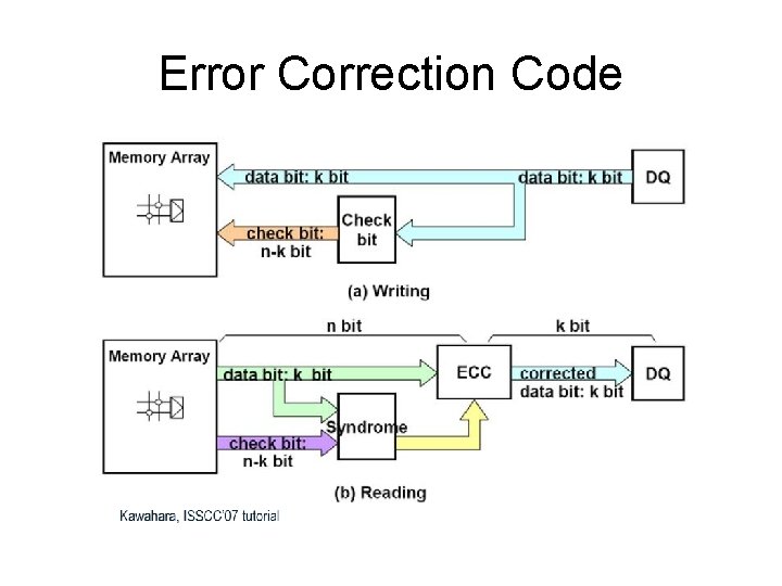
Error Correction Code

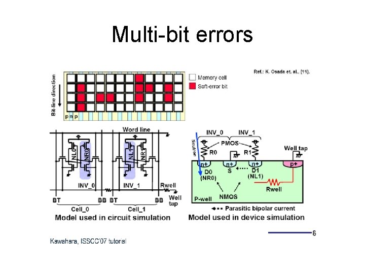
Multi-bit errors

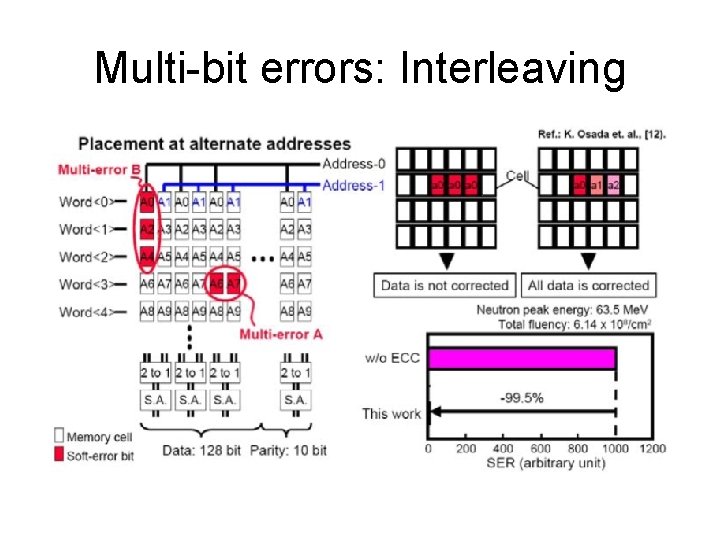
Multi-bit errors: Interleaving

Future trends • More than 6 T cells • Change in technology • e. DRAM

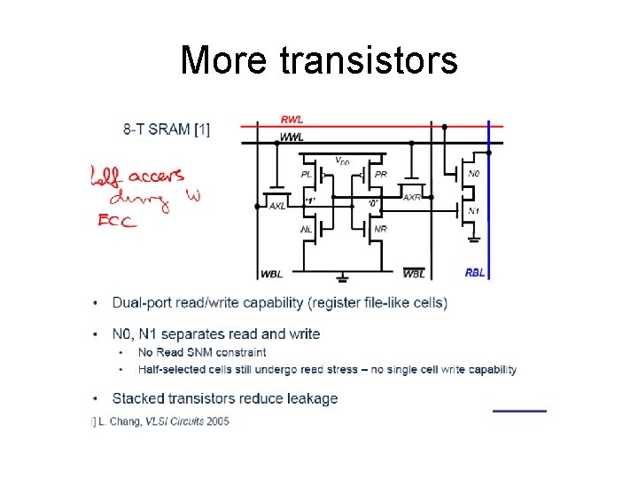
More transistors

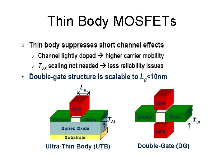
Thin Body MOSFETs

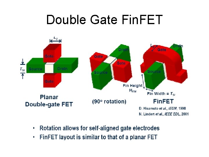
Double Gate Fin. FET

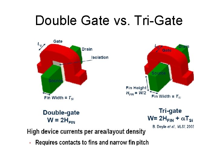
Double Gate vs. Tri-Gate

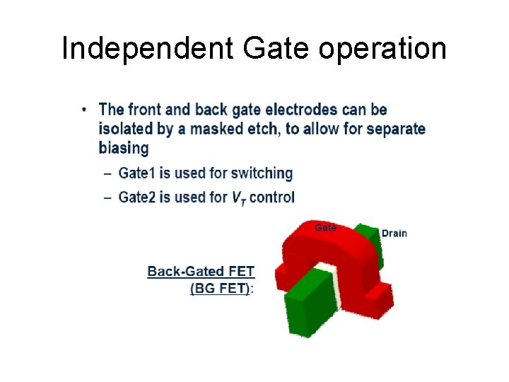
Independent Gate operation

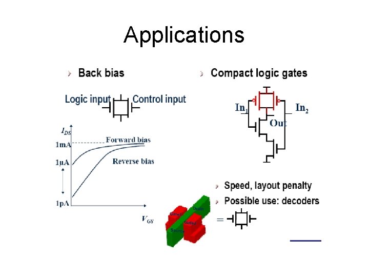
Applications

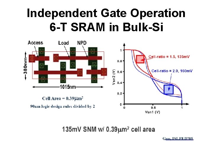
Independent Gate Operation 6 -T SRAM in Bulk-Si

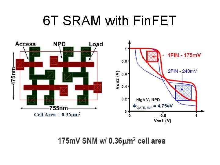
6 T SRAM with Fin. FET

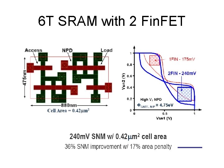
6 T SRAM with 2 Fin. FET

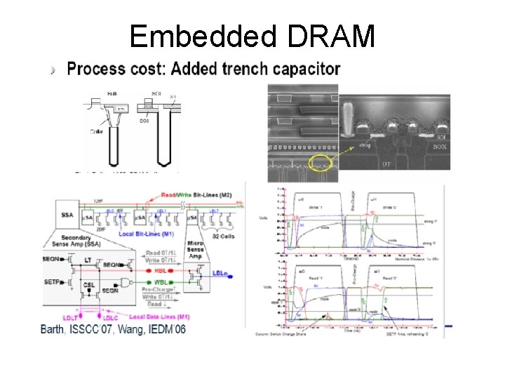
Embedded DRAM