Spin currents spinHall spin accumulation and anomalous Hall

- Slides: 56

Spin currents, spin-Hall spin accumulation, and anomalous Hall transport in strongly spin-orbit coupled systems Diluted Magnetic Semiconductors and Magnetization Dynamics ONR N 00014 -06 -1 -0122 JAIRO SINOVA Denver March 9 th 2007 Research fueled by:

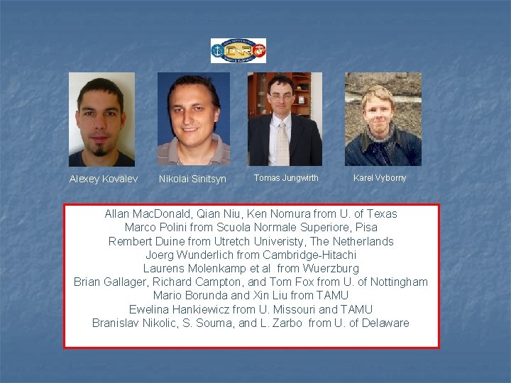
Alexey Kovalev Nikolai Sinitsyn Tomas Jungwirth Karel Vyborny Allan Mac. Donald, Qian Niu, Ken Nomura from U. of Texas Marco Polini from Scuola Normale Superiore, Pisa Rembert Duine from Utretch Univeristy, The Netherlands Joerg Wunderlich from Cambridge-Hitachi Laurens Molenkamp et al from Wuerzburg Brian Gallager, Richard Campton, and Tom Fox from U. of Nottingham Mario Borunda and Xin Liu from TAMU Ewelina Hankiewicz from U. Missouri and TAMU Branislav Nikolic, S. Souma, and L. Zarbo from U. of Delaware

ONR FUNDED TAMU SPIN PROGRAM ACTIVITY 2006 -2007 Spin and Anomalous Hall Effect: • N. A. Sinitsyn, et al, "Charge and spin Hall conductivity in metallic graphene", Phys. Rev. Lett. 97, 106804 (2006). • N. A. Sinitsyn, et al, "Anomalous Hall effect in 2 D Dirac band: link between Kubo-Streda formula and semiclassical Boltzmann equation approach", Phys. Rev. B 75, 045315 (2007). • Mario F. Borunda, et al, "Absence of skew scattering in two-dimensional systems: Testing the origins of the anomalous Hall Effect", pre-print: condmat/0702289, submitted to Phys. Rev. Lett. Diluted Magnetic Semiconductors/ Magnetization Dynamics: • T. Jungwirth, et al, "Theory of ferromagnetic (III, Mn)V Semiconductors", Rev. Mod. Phys. 78, 809 (2006) • J. Masek, et al, "Mn-doped Ga(As, P) and (Al, Ga)As ferromagnetic semiconductors", Phys. Rev. B 75, 045202 (2007). • J. Wunderlich, et al, “Local control of magnetocrystalline anisotropy in (Ga, Mn)As microdevices”, submitted to Phys. Rev. B • R. Duine, et al “Functional Keldysh Theory of spin-torques”, submitted to PRB Aharonov-Casher effect • M. Koenig, et al, "Direct observation of the Aharonov-Casher phase", Phys. Rev. Lett. 96, 076804 (2006). • Alexey A. Kovalev, et al "Aharonov-Casher effect in a two dimensional hole ring with spin-orbit interaction", pre-print: cond-mat/0701534, submitted to Phys. Rev. B

OUTLINE n Motivation: n n What is the problem Challenges and outlook: ITRS 2005 ONR Spintronics TAMU program Towards a comprehensive theory of anomalous transport: n The three spintronics Hall effects n n Anomalous Hall effect and Spin Hall effect n n n n AHE phenomenology and its long history Three contributions to the AHE Microscopic approach: focus on the intrinsic AHE Application to the SHE: theory, experiment, current status Equivalence of Kubo and Boltzmann: a success history of the Graphene model New results in 2 D-Rashba systems: absence of skew scattering Diluted Magnetic Semiconductors: towards a higher Tc n n Similarities and differences: why is it so difficult Experimental and theory trends of Tc Strategies to achieve higher Tc Using mathematical theorems to increase Tc A-C effect in mesoscopic rings with SO coupling

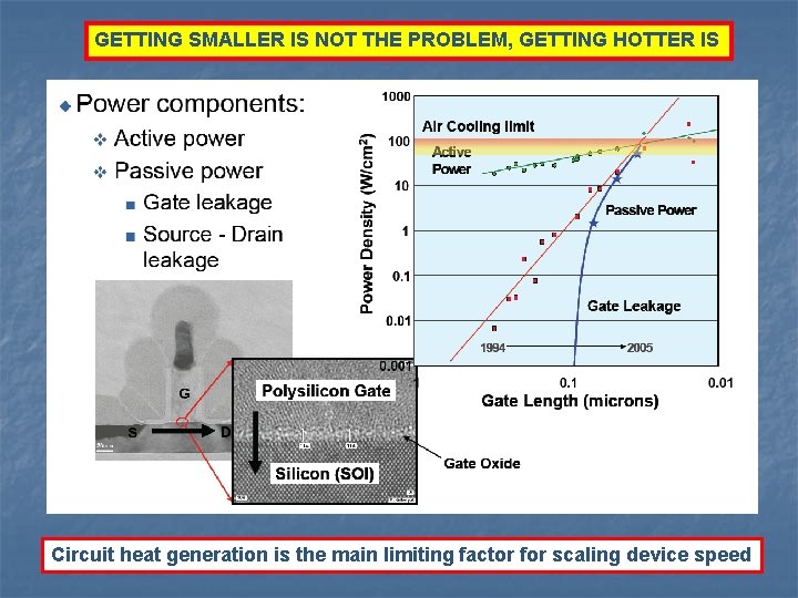
GETTING SMALLER IS NOT THE PROBLEM, GETTING HOTTER IS Circuit heat generation is the main limiting factor for scaling device speed

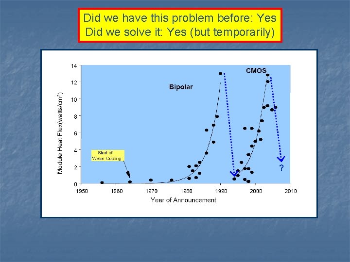
Did we have this problem before: Yes Did we solve it: Yes (but temporarily)

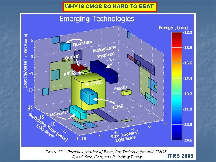
WHY IS CMOS SO HARD TO BEAT ITRS 2005

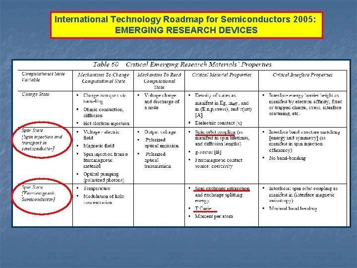
International Technology Roadmap for Semiconductors 2005: EMERGING RESEARCH DEVICES

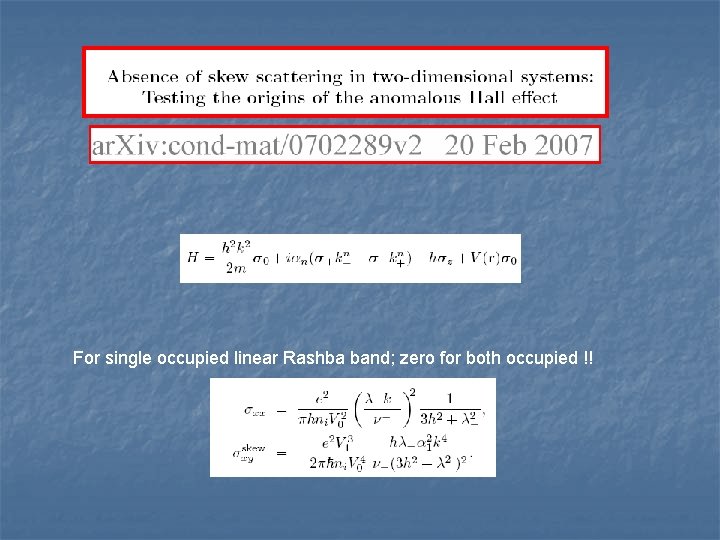
Spin and Anomalous Hall Effect: • N. A. Sinitsyn, et al, "Charge and spin Hall conductivity in metallic graphene", Phys. Rev. Lett. 97, 106804 (2006). • N. A. Sinitsyn, et al, "Anomalous Hall effect in 2 D Dirac band: link between Kubo-Streda formula and semiclassical Boltzmann equation approach", Phys. Rev. B 75, 045315 (2007). • Mario F. Borunda, et al, "Absence of skew scattering in two-dimensional systems: Testing the origins of the anomalous Hall Effect", pre-print: condmat/0702289, submitted to Phys. Rev. Lett.

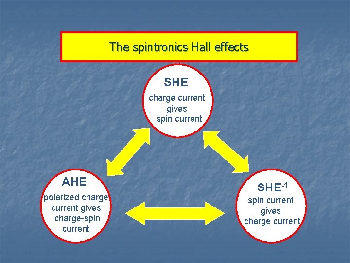
The spintronics Hall effects SHE charge current gives spin current AHE polarized charge current gives charge-spin current SHE-1 spin current gives charge current

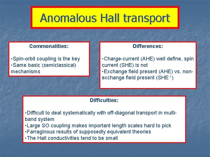
Anomalous Hall transport Commonalities: • Spin-orbit coupling is the key • Same basic (semiclassical) mechanisms Differences: • Charge-current (AHE) well define, spin current (SHE) is not • Exchange field present (AHE) vs. nonexchange field present (SHE-1) Difficulties: • Difficult to deal systematically with off-diagonal transport in multiband system • Large SO coupling makes important length scales hard to pick • Farraginous results of supposedly equivalent theories • The Hall conductivities tend to be small

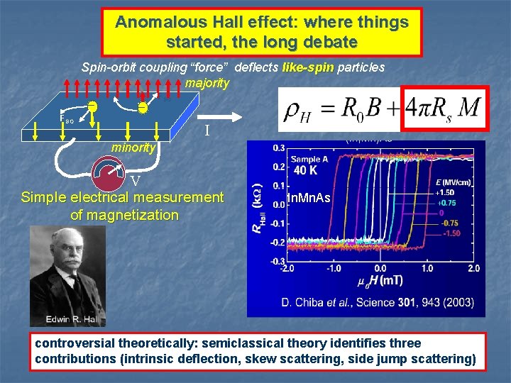
Anomalous Hall effect: where things started, the long debate Spin-orbit coupling “force” deflects like-spin particles majority __ FSO I minority V Simple electrical measurement of magnetization In. Mn. As controversial theoretically: semiclassical theory identifies three contributions (intrinsic deflection, skew scattering, side jump scattering)

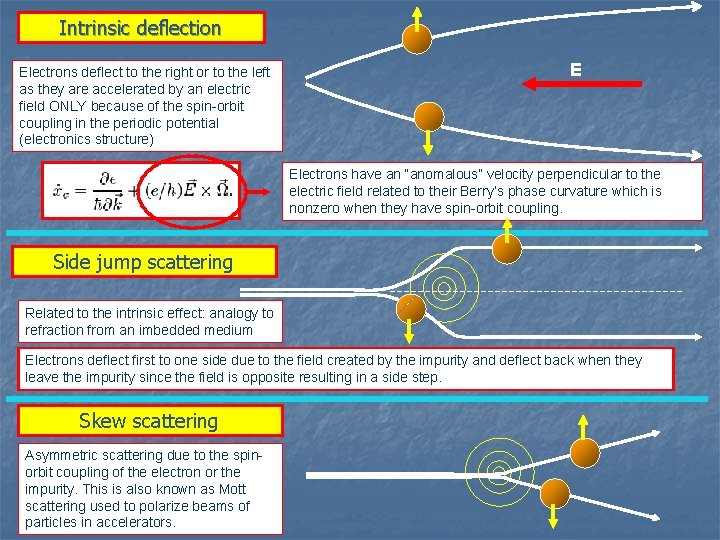
Intrinsic deflection Electrons deflect to the right or to the left as they are accelerated by an electric field ONLY because of the spin-orbit coupling in the periodic potential (electronics structure) E Electrons have an “anomalous” velocity perpendicular to the electric field related to their Berry’s phase curvature which is nonzero when they have spin-orbit coupling. Side jump scattering Related to the intrinsic effect: analogy to refraction from an imbedded medium Electrons deflect first to one side due to the field created by the impurity and deflect back when they leave the impurity since the field is opposite resulting in a side step. Skew scattering Asymmetric scattering due to the spinorbit coupling of the electron or the impurity. This is also known as Mott scattering used to polarize beams of particles in accelerators.

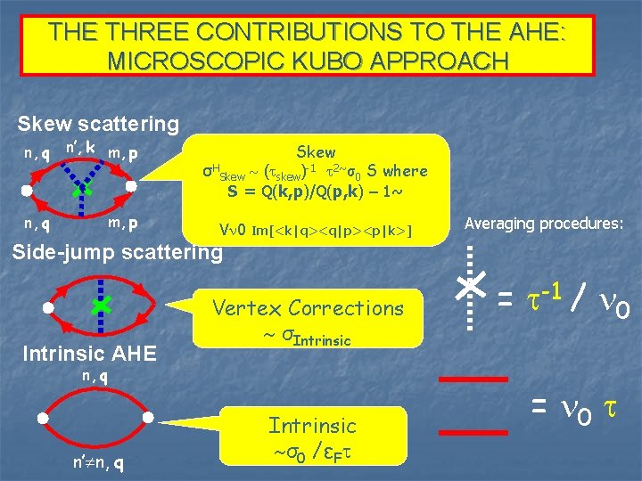
THE THREE CONTRIBUTIONS TO THE AHE: MICROSCOPIC KUBO APPROACH Skew scattering n, q n’, k m, p n, q m, p Skew σHSkew ( skew)-1 2~σ0 S where S = Q(k, p)/Q(p, k) – 1~ V 0 Im[<k|q><q|p><p|k>] Averaging procedures: Side-jump scattering Intrinsic AHE Vertex Corrections σIntrinsic n, q n’ n, q Intrinsic σ0 /εF = -1 / 0 = 0

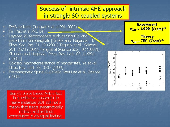
Success of intrinsic AHE approach in strongly SO coupled systems • • • DMS systems (Jungwirth et al PRL 2002) Fe (Yao et al PRL 04) Layered 2 D ferromagnets such as Sr. Ru. O 3 and pyrochlore ferromagnets [Onoda and Nagaosa, J. Phys. Soc. Jap. 71, 19 (2001), Taguchi et al. , Science 291, 2573 (2001), Fang et al Science 302, 92 (2003), Shindou and Nagaosa, Phys. Rev. Lett. 87, 116801 (2001)] Colossal magnetoresistance of manganites, Ye et~al Phys. Rev. Lett. 83, 3737 (1999). Ferromagnetic Spinel Cu. Cr. Se. Br: Wei-Lee et al, Science (2004) Berry’s phase based AHE effect is quantitative-successful in many instances BUT still not a theory that treats systematically intrinsic and extrinsic contribution in an equal footing. Experiment s. AH 1000 (W cm)-1 Theroy s. AH 750 (W cm)-1

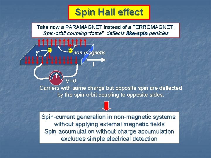
Spin Hall effect Take now a PARAMAGNET instead of a FERROMAGNET: Spin-orbit coupling “force” deflects like-spin particles _ FSO __ FSO non-magnetic I V=0 Carriers with same charge but opposite spin are deflected by the spin-orbit coupling to opposite sides. Spin-current generation in non-magnetic systems without applying external magnetic fields Spin accumulation without charge accumulation excludes simple electrical detection

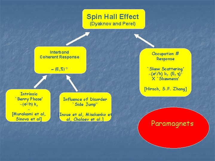
Spin Hall Effect (Dyaknov and Perel) Interband Coherent Response Occupation # Response (EF ) 0 `Skew Scattering‘ (e 2/h) k. F (EF )1 X `Skewness’ Intrinsic `Berry Phase’ (e 2/h) k. F [Murakami et al, Sinova et al] [Hirsch, S. F. Zhang] Influence of Disorder `Side Jump’’ [Inoue et al, Misckenko et al, Chalaev et al. ] Paramagnets

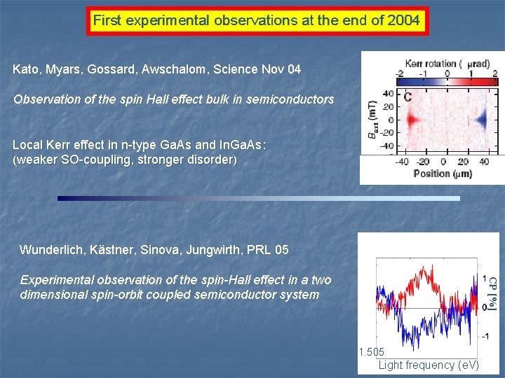
First experimental observations at the end of 2004 Kato, Myars, Gossard, Awschalom, Science Nov 04 Observation of the spin Hall effect bulk in semiconductors Local Kerr effect in n-type Ga. As and In. Ga. As: (weaker SO-coupling, stronger disorder) 1. 52 Wunderlich, Kästner, Sinova, Jungwirth, PRL 05 CP [%] Experimental observation of the spin-Hall effect in a two dimensional spin-orbit coupled semiconductor system 1. 505 Light frequency (e. V)

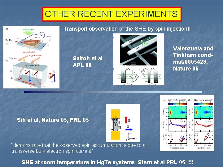
OTHER RECENT EXPERIMENTS Transport observation of the SHE by spin injection!! Saitoh et al APL 06 Valenzuela and Tinkham condmat/0605423, Nature 06 Sih et al, Nature 05, PRL 05 “demonstrate that the observed spin accumulation is due to a transverse bulk electron spin current” SHE at room temperature in Hg. Te systems Stern et al PRL 06 !!!

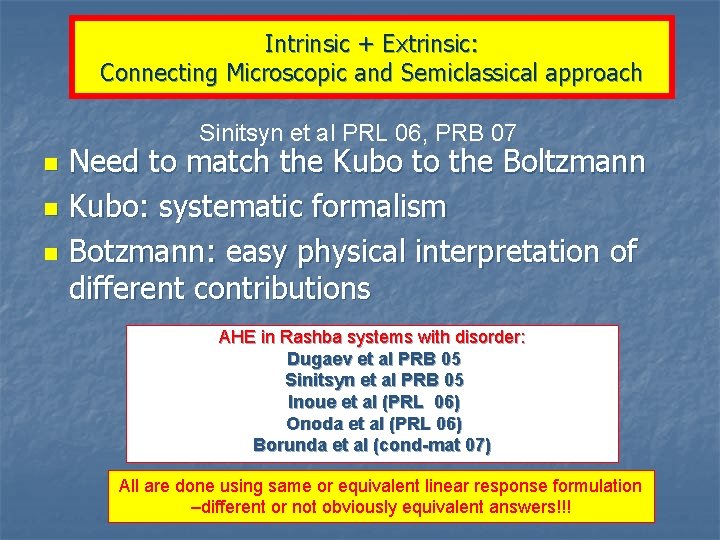
Intrinsic + Extrinsic: Connecting Microscopic and Semiclassical approach Sinitsyn et al PRL 06, PRB 07 n n n Need to match the Kubo to the Boltzmann Kubo: systematic formalism Botzmann: easy physical interpretation of different contributions AHE in Rashba systems with disorder: Dugaev et al PRB 05 Sinitsyn et al PRB 05 Inoue et al (PRL 06) Onoda et al (PRL 06) Borunda et al (cond-mat 07) All are done using same or equivalent linear response formulation –different or not obviously equivalent answers!!!

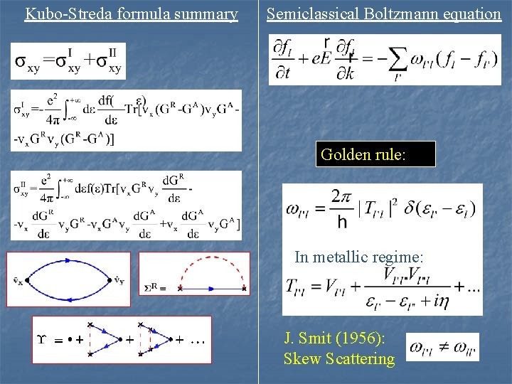
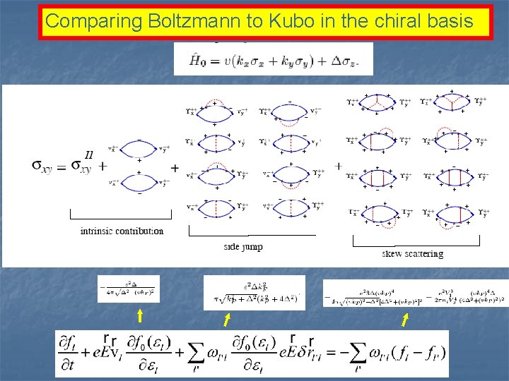
Kubo-Streda formula summary Semiclassical Boltzmann equation Golden rule: In metallic regime: J. Smit (1956): Skew Scattering

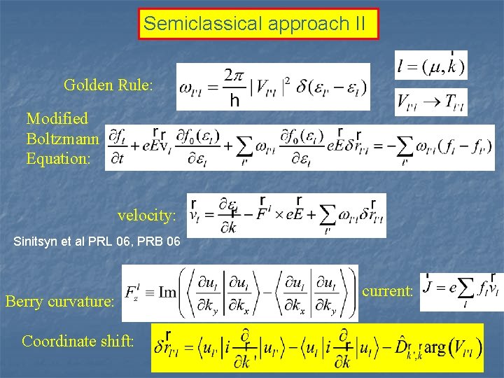
Semiclassical approach II Golden Rule: Modified Boltzmann Equation: velocity: Sinitsyn et al PRL 06, PRB 06 Berry curvature: Coordinate shift: current:

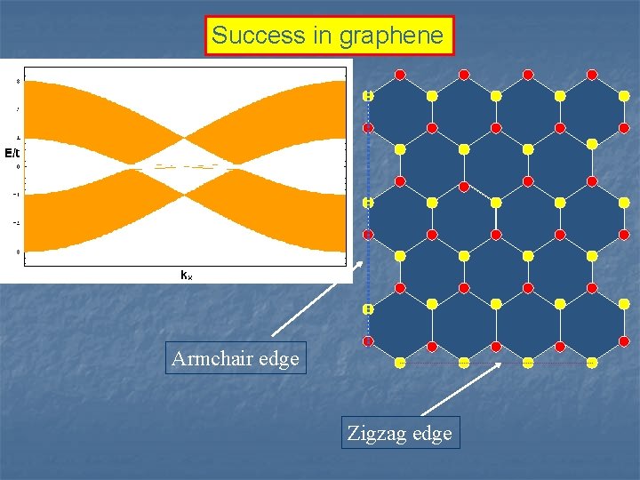
Success in graphene EF Armchair edge Zigzag edge

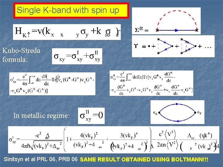
Single K-band with spin up Kubo-Streda formula: In metallic regime: Sinitsyn et al PRL 06, PRB 06 SAME RESULT OBTAINED USING BOLTMANN!!!

Comparing Boltzmann to Kubo in the chiral basis

For single occupied linear Rashba band; zero for both occupied !!

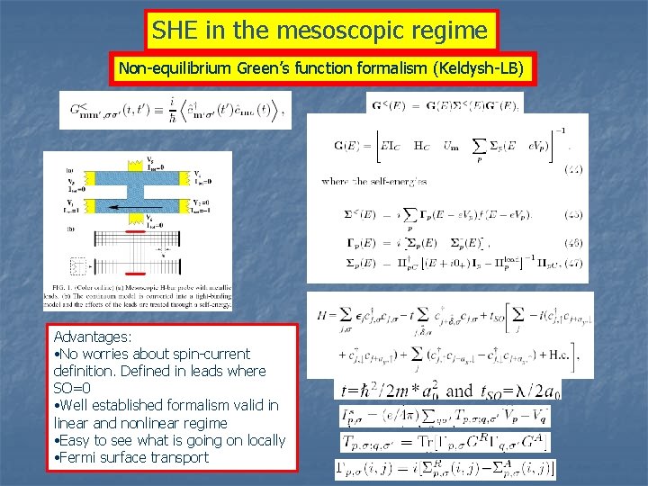
SHE in the mesoscopic regime Non-equilibrium Green’s function formalism (Keldysh-LB) Advantages: • No worries about spin-current definition. Defined in leads where SO=0 • Well established formalism valid in linear and nonlinear regime • Easy to see what is going on locally • Fermi surface transport

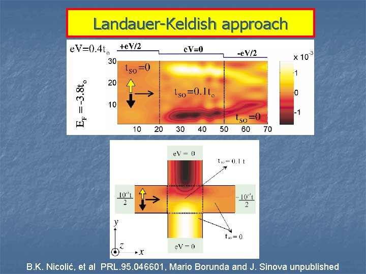
Landauer-Keldish approach B. K. Nicolić, et al PRL. 95. 046601, Mario Borunda and J. Sinova unpublished

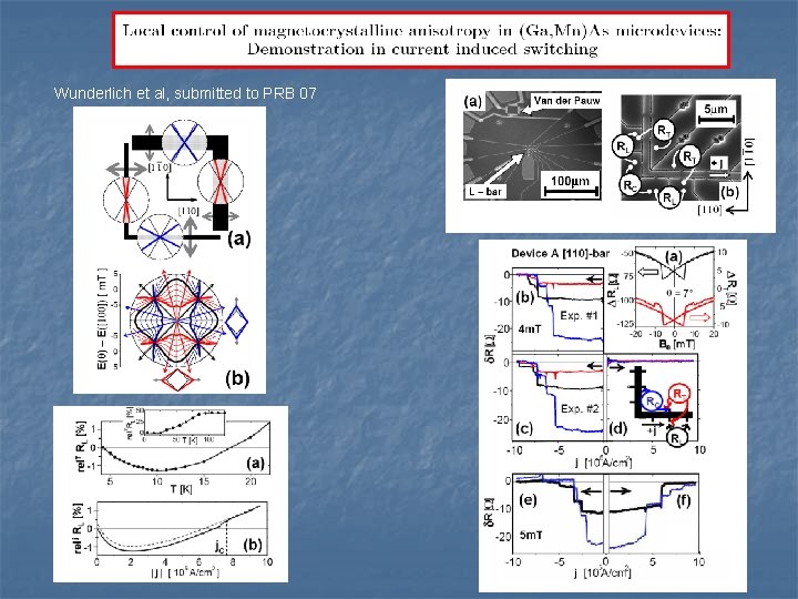
Diluted Magnetic Semiconductors/ Magnetization Dynamics • T. Jungwirth, et al, "Theory of ferromagnetic (III, Mn)V Semiconductors", Rev. Mod. Phys. 78, 809 (2006) • J. Masek, et al, "Mn-doped Ga(As, P) and (Al, Ga)As ferromagnetic semiconductors", Phys. Rev. B 75, 045202 (2007). • J. Wunderlich, et al, “Local control of magnetocrystalline anisotropy in (Ga, Mn)As microdevices”, submitted to Phys. Rev. B • R. Duine, et al “Functional Keldysh Theory of spin-torques”, submitted to PRB

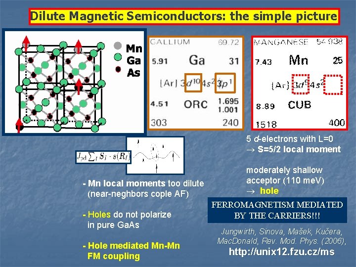
Dilute Magnetic Semiconductors: the simple picture 5 d-electrons with L=0 S=5/2 local moment - Mn local moments too dilute (near-neghbors cople AF) - Holes do not polarize in pure Ga. As - Hole mediated Mn-Mn FM coupling moderately shallow acceptor (110 me. V) hole FERROMAGNETISM MEDIATED BY THE CARRIERS!!! Jungwirth, Sinova, Mašek, Kučera, Mac. Donald, Rev. Mod. Phys. (2006), http: //unix 12. fzu. cz/ms

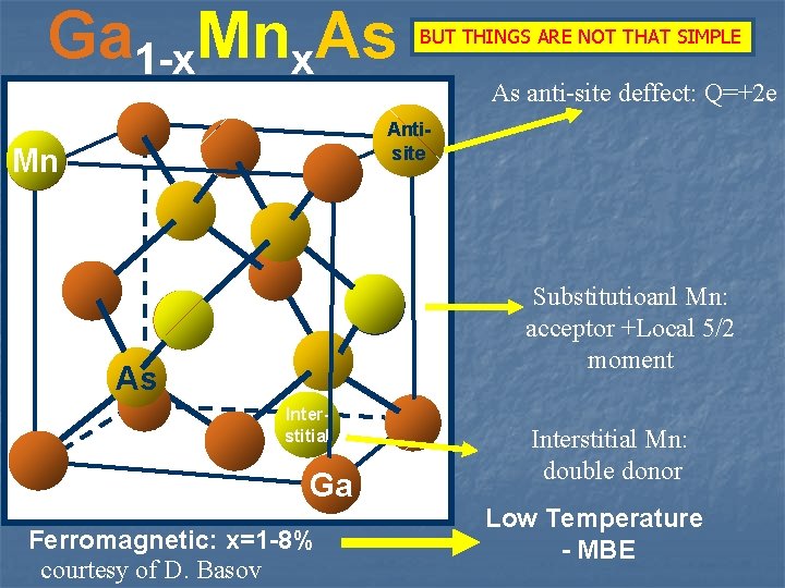
Ga 1 -x. Mnx. As BUT THINGS ARE NOT THAT SIMPLE As anti-site deffect: Q=+2 e Antisite Mn Substitutioanl Mn: acceptor +Local 5/2 moment As Interstitial Ga Ferromagnetic: x=1 -8% courtesy of D. Basov Interstitial Mn: double donor Low Temperature - MBE

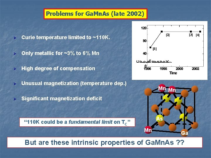
Problems for Ga. Mn. As (late 2002) Ø Curie temperature limited to ~110 K. Ø Only metallic for ~3% to 6% Mn Ø High degree of compensation Ø Unusual magnetization (temperature dep. ) Ø Significant magnetization deficit Mn Mn As “ 110 K could be a fundamental limit on TC” Mn Ga But are these intrinsic properties of Ga. Mn. As ? ?

Can a dilute moment ferromagnet have a high Curie temperature ? The questions that we need to answer are: 1. Is there an intrinsic limit in theory models (from the physics of the phase diagram) ? 2. Is there an extrinsic limit from the ability to create the material and its growth (prevents one to reach the optimal spot in the phase diagram)?

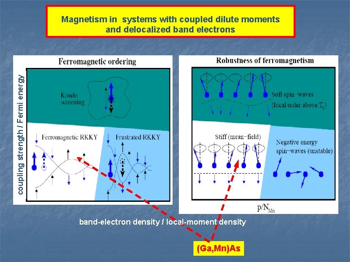
coupling strength / Fermi energy Magnetism in systems with coupled dilute moments and delocalized band electrons band-electron density / local-moment density (Ga, Mn)As

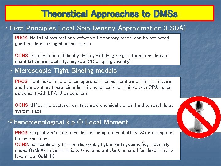
Theoretical Approaches to DMSs • First Principles Local Spin Density Approximation (LSDA) PROS: No initial assumptions, effective Heisenberg model can be extracted, good for determining chemical trends CONS: Size limitation, difficulty dealing with long range interactions, lack of quantitative predictability, neglects SO coupling (usually) • Microscopic Tight Binding models PROS: “Unbiased” microscopic approach, correct capture of band structure and hybridization, treats disorder microscopically (combined with CPA), good agreement with LDA+U calculations CONS: difficult to capture non-tabulated chemical trends, hard to reach large system sizes • Phenomenological k. p Local Moment PROS: simplicity of description, lots of computational ability, SO coupling can be incorporated, CONS: applicable only for metallic weakly hybridized systems (e. g. optimally doped Ga. Mn. As), over simplicity (e. g. constant Jpd), no good for deep impurity levels (e. g. Ga. Mn. N)

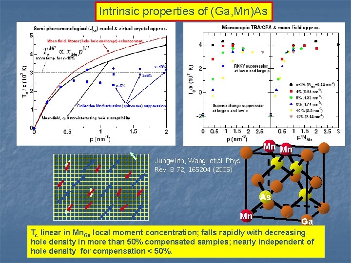
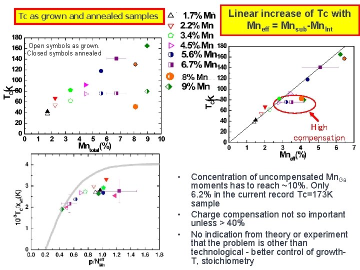
Intrinsic properties of (Ga, Mn)As Mn Mn Jungwirth, Wang, et al. Phys. Rev. B 72, 165204 (2005) As Mn Ga Tc linear in Mn. Ga local moment concentration; falls rapidly with decreasing hole density in more than 50% compensated samples; nearly independent of hole density for compensation < 50%.

Linear increase of Tc with Mneff = Mnsub-Mn. Int Tc as grown and annealed samples Open symbols as grown. Closed symbols annealed 8% Mn High compensation • • • Concentration of uncompensated Mn. Ga moments has to reach ~10%. Only 6. 2% in the current record Tc=173 K sample Charge compensation not so important unless > 40% No indication from theory or experiment that the problem is other than technological - better control of growth. T, stoichiometry

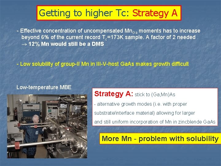
Getting to higher Tc: Strategy A - Effective concentration of uncompensated Mn. Ga moments has to increase beyond 6% of the current record Tc=173 K sample. A factor of 2 needed 12% Mn would still be a DMS - Low solubility of group-II Mn in III-V-host Ga. As makes growth difficult Low-temperature MBE Strategy A: stick to (Ga, Mn)As - alternative growth modes (i. e. with proper substrate/interface material) allowing for larger and still uniform incorporation of Mn in zincblende Ga. As More Mn - problem with solubility

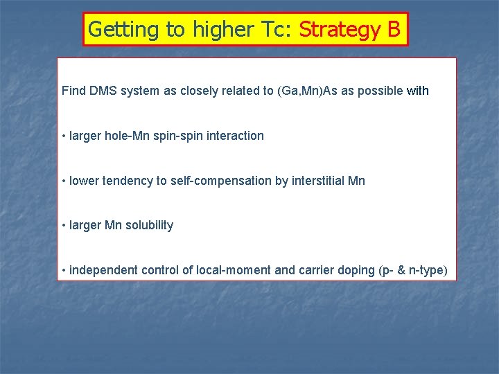
Getting to higher Tc: Strategy B Find DMS system as closely related to (Ga, Mn)As as possible with • larger hole-Mn spin-spin interaction • lower tendency to self-compensation by interstitial Mn • larger Mn solubility • independent control of local-moment and carrier doping (p- & n-type)

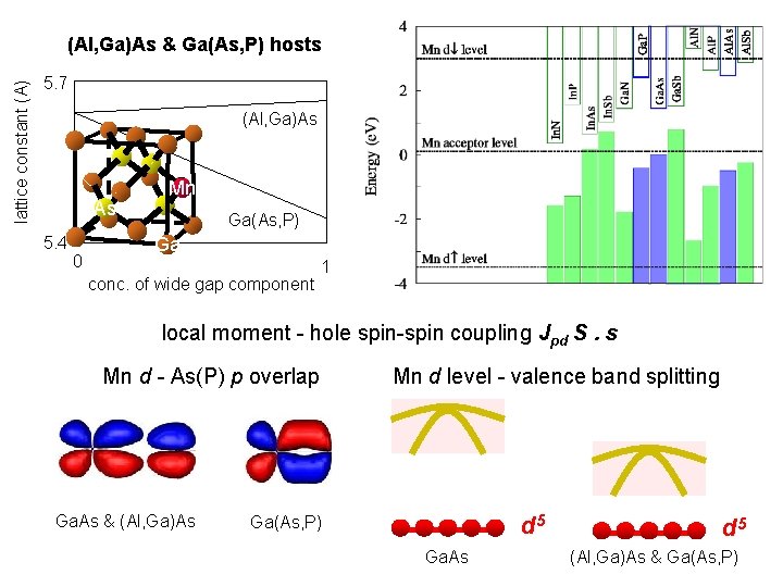
lattice constant (A) (Al, Ga)As & Ga(As, P) hosts 5. 7 (Al, Ga)As As 5. 4 0 Mn Ga(As, P) Ga conc. of wide gap component 1 local moment - hole spin-spin coupling Jpd S. s Mn d - As(P) p overlap Ga. As & (Al, Ga)As Mn d level - valence band splitting d 5 Ga(As, P) Ga. As d 5 (Al, Ga)As & Ga(As, P)

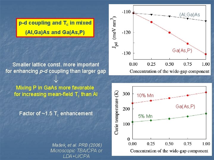
(Al, Ga)As p-d coupling and Tc in mixed (Al, Ga)As and Ga(As, P) 10% Mn theory Ga(As, P) Smaller lattice const. more important for enhancing p-d coupling than larger gap Mixing P in Ga. As more favorable for increasing mean-field Tc than Al 10% Mn Ga(As, P) Factor of ~1. 5 Tc enhancement 5% Mn theory Mašek, et al. PRB (2006) Microscopic TBA/CPA or LDA+U/CPA

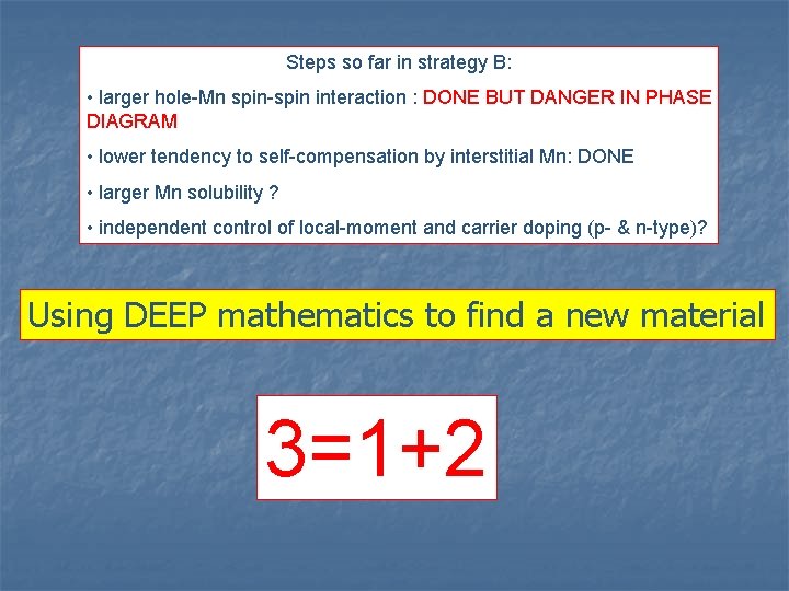
Steps so far in strategy B: • larger hole-Mn spin-spin interaction : DONE BUT DANGER IN PHASE DIAGRAM • lower tendency to self-compensation by interstitial Mn: DONE • larger Mn solubility ? • independent control of local-moment and carrier doping (p- & n-type)? Using DEEP mathematics to find a new material 3=1+2

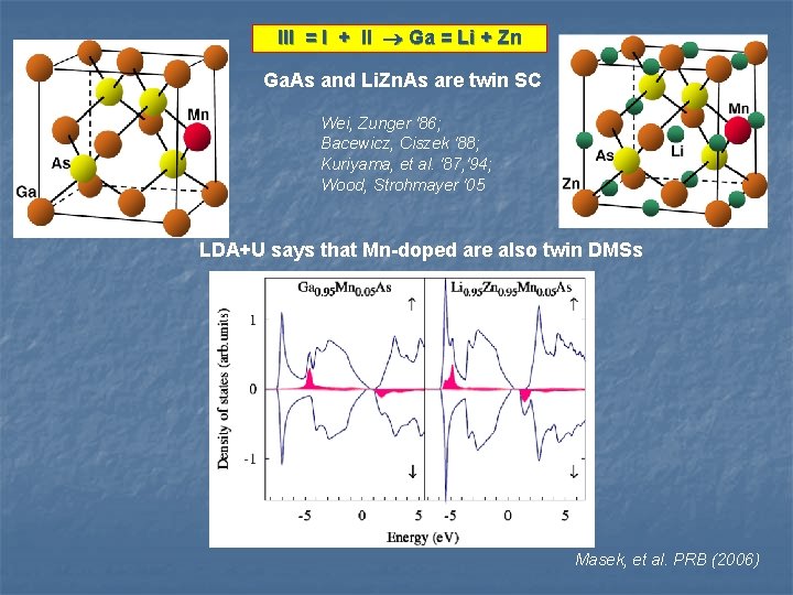
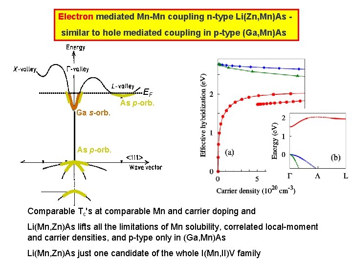
III = I + II Ga = Li + Zn Ga. As and Li. Zn. As are twin SC Wei, Zunger '86; Bacewicz, Ciszek '88; Kuriyama, et al. '87, '94; Wood, Strohmayer '05 LDA+U says that Mn-doped are also twin DMSs Masek, et al. PRB (2006)

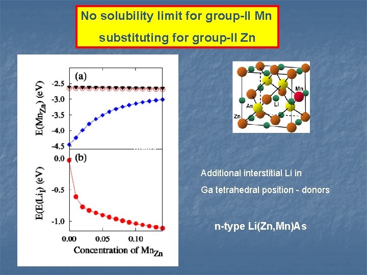
No solubility limit for group-II Mn substituting for group-II Zn theory Additional interstitial Li in Ga tetrahedral position - donors n-type Li(Zn, Mn)As

Electron mediated Mn-Mn coupling n-type Li(Zn, Mn)As similar to hole mediated coupling in p-type (Ga, Mn)As EF As p-orb. Ga s-orb. L As p-orb. Comparable Tc's at comparable Mn and carrier doping and Li(Mn, Zn)As lifts all the limitations of Mn solubility, correlated local-moment and carrier densities, and p-type only in (Ga, Mn)As Li(Mn, Zn)As just one candidate of the whole I(Mn, II)V family

Wunderlich et al, submitted to PRB 07

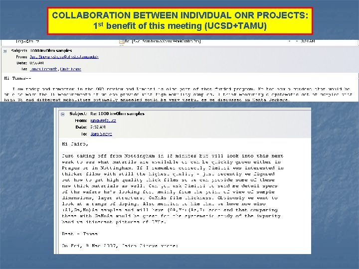
COLLABORATION BETWEEN INDIVIDUAL ONR PROJECTS: 1 st benefit of this meeting (UCSD+TAMU)

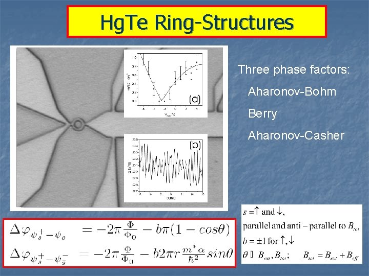
Aharonov-Casher effect: corollary of Aharonov-Bohm effect with electric fields instead • M. Koenig, et al, "Direct observation of the Aharonov-Casher phase", Phys. Rev. Lett. 96, 076804 (2006). • Alexey A. Kovalev, et al "Aharonov-Casher effect in a two dimensional hole ring with spin-orbit interaction", pre-print: cond-mat/0701534, submitted to Phys. Rev. B Control of conductance through a novel Berry’s phase effect induced by gate voltages instead of magnetic fields

Hg. Te Ring-Structures Three phase factors: Aharonov-Bohm Berry Aharonov-Casher

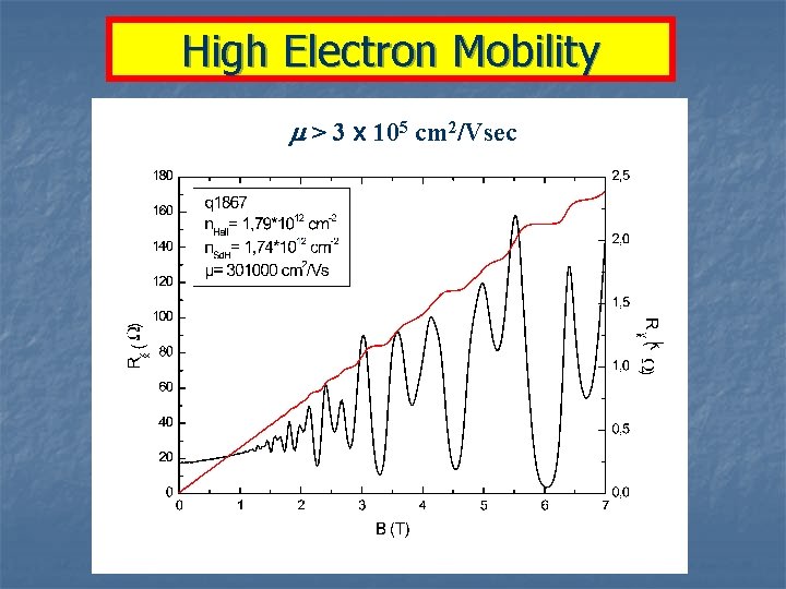
High Electron Mobility m > 3 x 105 cm 2/Vsec

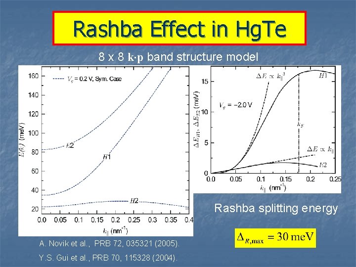
Rashba Effect in Hg. Te 8 x 8 k×p band structure model Rashba splitting energy A. Novik et al. , PRB 72, 035321 (2005). Y. S. Gui et al. , PRB 70, 115328 (2004).

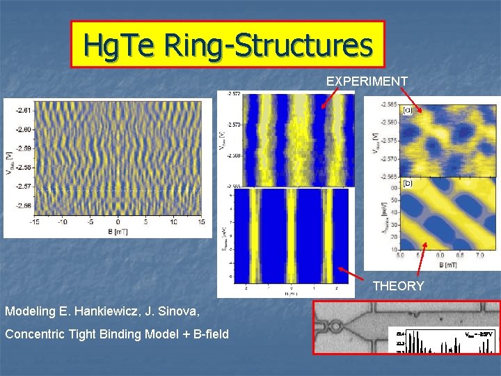
Hg. Te Ring-Structures EXPERIMENT THEORY Modeling E. Hankiewicz, J. Sinova, Concentric Tight Binding Model + B-field

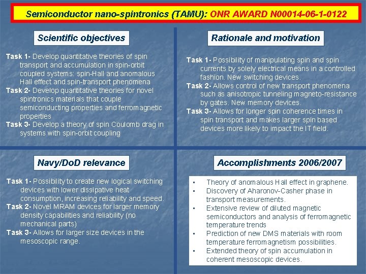
Semiconductor nano-spintronics (TAMU): ONR AWARD N 00014 -06 -1 -0122 Scientific objectives Task 1 - Develop quantitative theories of spin transport and accumulation in spin-orbit coupled systems: spin-Hall and anomalous Hall effect and spin-transport phenomena Task 2 - Develop quantitative theories for novel spintronics materials that couple semiconducting properties and ferromagnetic properties Task 3 - Develop a theory of spin Coulomb drag in systems with spin-orbit coupling Rationale and motivation Task 1 - Possibility of manipulating spin and spin currents by solely electrical means in a controlled fashion. New switching devices. Task 2 - Allows control of new transport phenomena such as anisotropic tunneling magneto-resistance by gates. New memory devices. Task 3 - Allows for longer spin coherence times in spin transport and makes larger spin based devices more likely to impact the IT field. Navy/Do. D relevance Task 1 - Possibility to create new logical switching devices with lower dissipative heat consumption, increasing reliability and speed. Task 2 - Novel MRAM devices for larger memory density capabilities and reliability (no mechanical parts) Task 3 - Allows for larger size devices in the mesoscopic range. Accomplishments 2006/2007 • • • Theory of anomalous Hall effect in graphene. Discovery of Aharonov-Casher phase in transport measurements. Extensive review of diluted magnetic semiconductors and analysis of ferromagnetic temperature trends Prediction of new DMS materials with room temperature ferromagnetism possibilities. Extended theory of spin accumulation in coherent mesoscopic devices.

EXTRAS

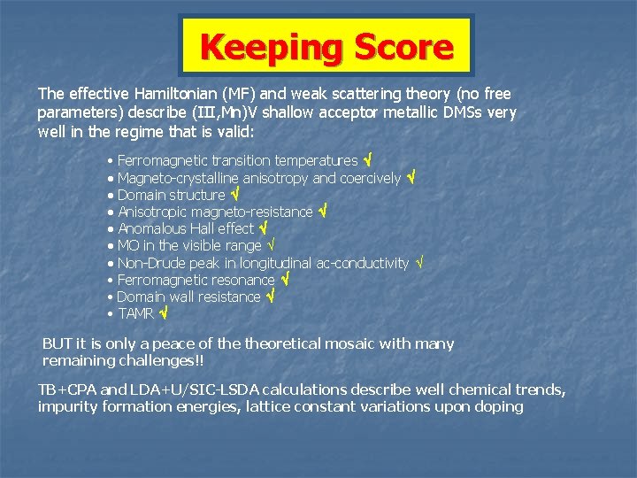
Keeping Score The effective Hamiltonian (MF) and weak scattering theory (no free parameters) describe (III, Mn)V shallow acceptor metallic DMSs very well in the regime that is valid: • Ferromagnetic transition temperatures Magneto-crystalline anisotropy and coercively Domain structure Anisotropic magneto-resistance Anomalous Hall effect MO in the visible range Non-Drude peak in longitudinal ac-conductivity • Ferromagnetic resonance • Domain wall resistance • TAMR BUT it is only a peace of theoretical mosaic with many remaining challenges!! TB+CPA and LDA+U/SIC-LSDA calculations describe well chemical trends, impurity formation energies, lattice constant variations upon doping

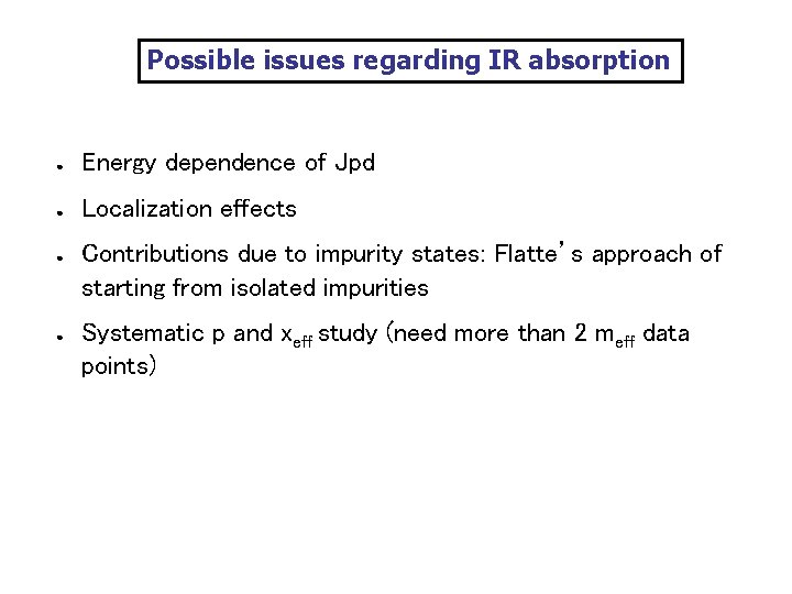
Possible issues regarding IR absorption ● Energy dependence of Jpd ● Localization effects ● ● Contributions due to impurity states: Flatte’s approach of starting from isolated impurities Systematic p and xeff study (need more than 2 meff data points)