SPI PROTOCOL TIMIR SONI AGENDA Introduction and Characteristics


- Slides: 18

SPI PROTOCOL TIMIR SONI

AGENDA • Introduction and Characteristics • SPI Operation • SPI I/O Registers • SPI Modes • Topology • Register Summary • Limitation • I 2 C v/s SPI 2

Introduction • The name SPI stands for “Serial Peripheral Interface” • Developed by Motorola • Also known as Micro-Wire • Networks multiple microcontrollers with 3 wires. • Allow microcontrollers communicate with each other. • High speed, real-time communication. • Low cost • Synchronous: No need of Start bit, Stop bit. • Simple communication hardware(Shift register) • Easily expandable since the clock is controlled by the master only • Full duplex single byte format • Fast communication 3

SPI Operation • For SPI, there are Serial Clocks (SCLK), Chip Select lines (CS)(also known as Slave Select), Serial Data In (SDI) and Serial Data Out( SDO) • There is only one master, the number of slaves depends on the number of chip select lines of the master. • Synchronous operation, latch on rising or falling edge of clock, SDI on rising edge, SDO on falling edge • Operates in 1 to 10 MHz range • Master sends out common clock and chip select. Activates the slaves it wants to communicate with. 4

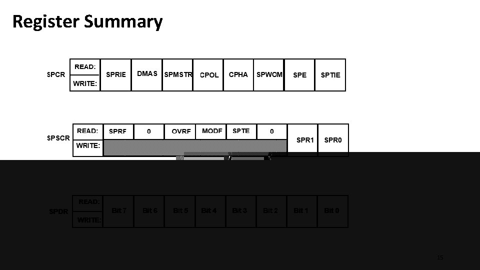
SPI I/O Registers • Three registers control and monitor SPI operations: - SPI Control Register (SPCR) - SPI Status and Control Register (SPSCR) - SPI Data Register (SPDR) 5

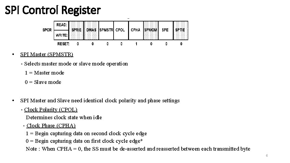
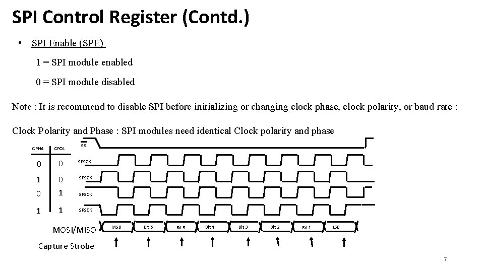
SPI Control Register • SPI Master (SPMSTR) - Selects master mode or slave mode operation 1 = Master mode 0 = Slave mode • SPI Master and Slave need identical clock polarity and phase settings - Clock Polarity (CPOL) Determines clock state when idle - Clock Phase (CPHA) 1 = Begin capturing data on second clock cycle edge 0 = Begin capturing data on first clock cycle edge* Note : When CPHA = 0, the SS must be de-asserted and reasserted between each transmitted byte 6

SPI Control Register (Contd. ) • SPI Enable (SPE) 1 = SPI module enabled 0 = SPI module disabled Note : It is recommend to disable SPI before initializing or changing clock phase, clock polarity, or baud rate : Clock Polarity and Phase : SPI modules need identical Clock polarity and phase SS CPHA CPOL 0 0 SPSCK 1 SPSCK 0 0 1 1 1 SPSCK MOSI/MISO MSB Bit 6 Bit 5 Bit 4 Bit 3 Bit 2 Bit 1 LSB Capture Strobe 7

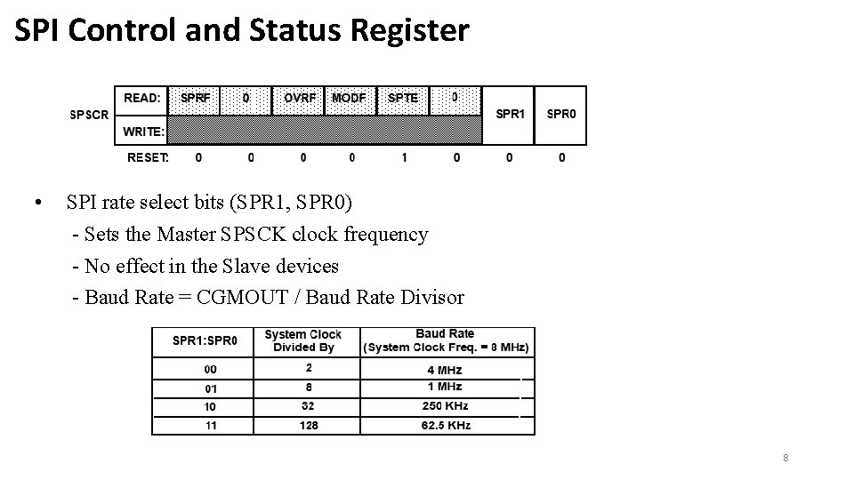
SPI Control and Status Register • SPI rate select bits (SPR 1, SPR 0) - Sets the Master SPSCK clock frequency - No effect in the Slave devices - Baud Rate = CGMOUT / Baud Rate Divisor 8

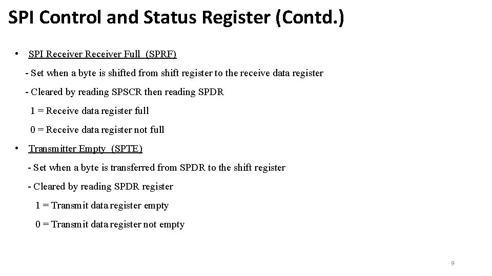
SPI Control and Status Register (Contd. ) • SPI Receiver Full (SPRF) - Set when a byte is shifted from shift register to the receive data register - Cleared by reading SPSCR then reading SPDR 1 = Receive data register full 0 = Receive data register not full • Transmitter Empty (SPTE) - Set when a byte is transferred from SPDR to the shift register - Cleared by reading SPDR register 1 = Transmit data register empty 0 = Transmit data register not empty 9

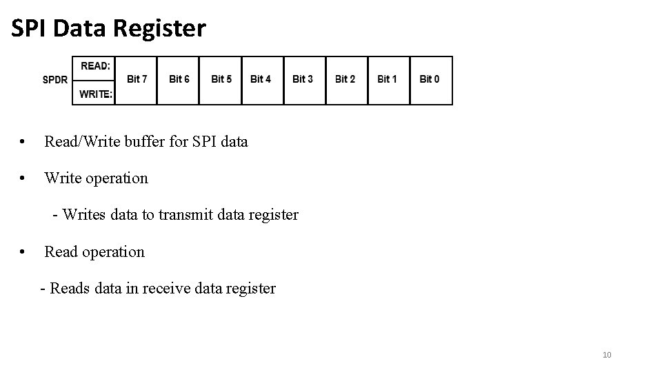
SPI Data Register • Read/Write buffer for SPI data • Write operation - Writes data to transmit data register • Read operation - Reads data in receive data register 10

SPI Modes • Master mode - Only a master initiates a transmission - Data is shifted out via Master Out Slave In (MOSI) line - Data is shifted in via Master In Slave Out (MISO) line - Transmission ends after 8 cycles of serial clock (SPSCK) • Slave Mode - Transfer synchronized to serial clock (SPSCK) from Master - Data is shifted in via the Master Out Slave In (MOSI) line - Data is shifted out via the Master In Slave Out (MISO) line 11

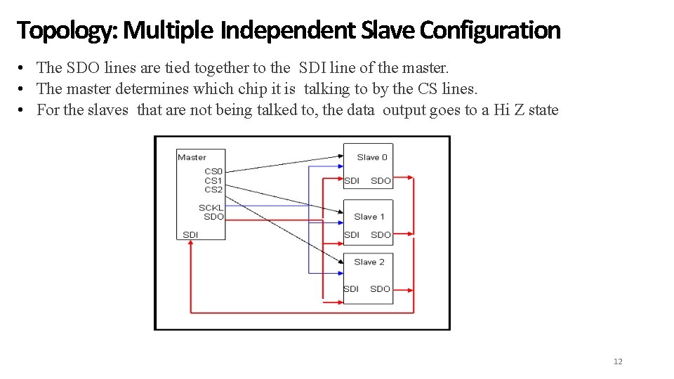
Topology: Multiple Independent Slave Configuration • The SDO lines are tied together to the SDI line of the master. • The master determines which chip it is talking to by the CS lines. • For the slaves that are not being talked to, the data output goes to a Hi Z state 12

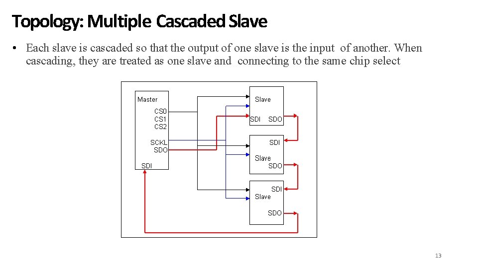
Topology: Multiple Cascaded Slave • Each slave is cascaded so that the output of one slave is the input of another. When cascading, they are treated as one slave and connecting to the same chip select 13

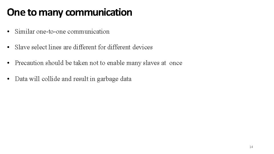
One to many communication • Similar one-to-one communication • Slave select lines are different for different devices • Precaution should be taken not to enable many slaves at once • Data will collide and result in garbage data 14

Register Summary 15

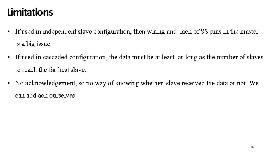
Limitations • If used in independent slave configuration, then wiring and lack of SS pins in the master is a big issue. • If used in cascaded configuration, the data must be at least as long as the number of slaves to reach the farthest slave. • No acknowledgement, so no way of knowing whether slave received the data or not. We can add ack ourselves 16

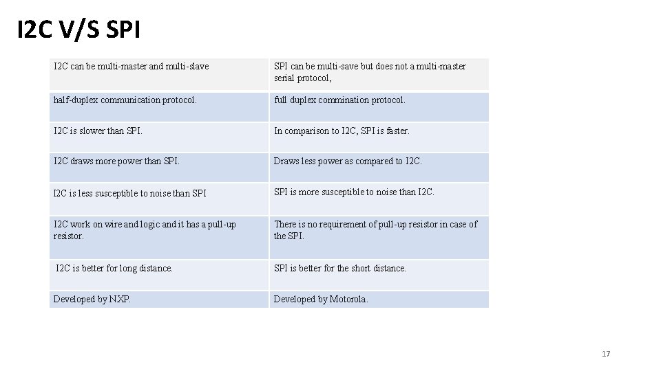
I 2 C V/S SPI I 2 C can be multi-master and multi-slave SPI can be multi-save but does not a multi-master serial protocol, half-duplex communication protocol. full duplex commination protocol. I 2 C is slower than SPI. In comparison to I 2 C, SPI is faster. I 2 C draws more power than SPI. Draws less power as compared to I 2 C is less susceptible to noise than SPI is more susceptible to noise than I 2 C work on wire and logic and it has a pull-up resistor. There is no requirement of pull-up resistor in case of the SPI. I 2 C is better for long distance. SPI is better for the short distance. Developed by NXP. Developed by Motorola. 17

18