SPI Protocol Sepehr Naimi www Nicer Land com

- Slides: 22

SPI Protocol Sepehr Naimi www. Nicer. Land. com

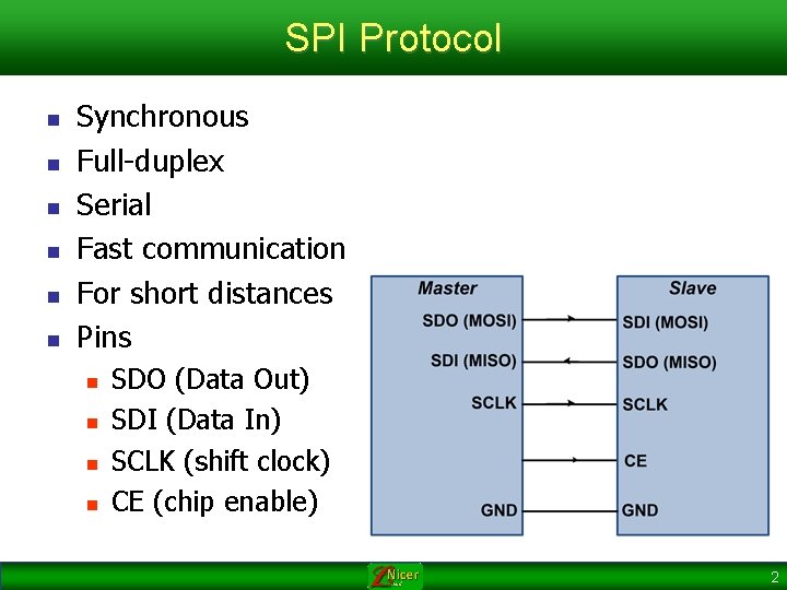
SPI Protocol n n n Synchronous Full-duplex Serial Fast communication For short distances Pins n n SDO (Data Out) SDI (Data In) SCLK (shift clock) CE (chip enable) 2

Master vs. Slave n n Master begins the communication by pulling down the CE pin of slave. Master makes the clock for communication 3

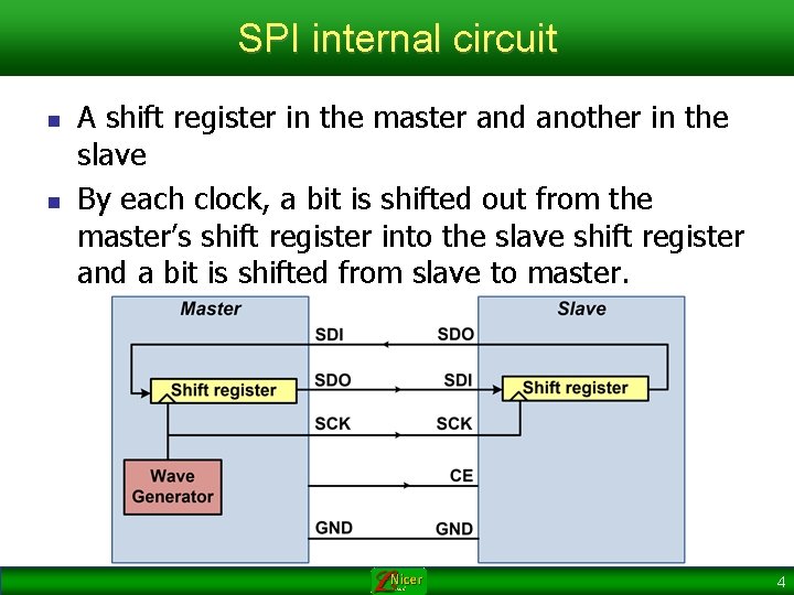
SPI internal circuit n n A shift register in the master and another in the slave By each clock, a bit is shifted out from the master’s shift register into the slave shift register and a bit is shifted from slave to master. 4

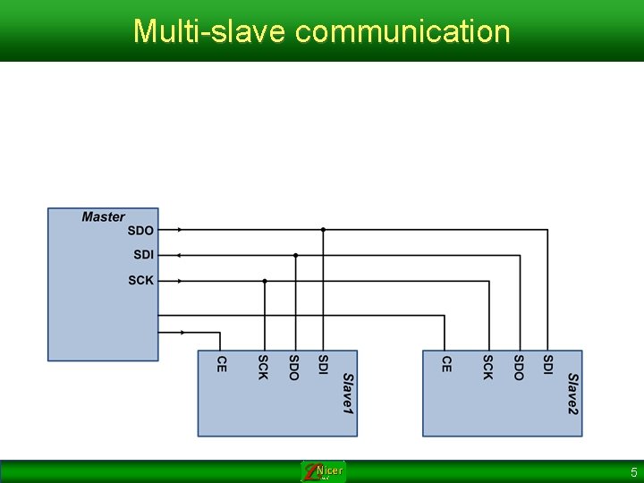
Multi-slave communication 5

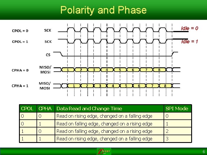
Polarity and Phase Idle = 0 Idle = 1 CPOL CPHA Data Read and Change Time SPI Mode 0 0 Read on rising edge, changed on a falling edge 0 0 1 Read on falling edge, changed on a rising edge 1 1 0 Read on falling edge, changed on a rising edge 2 1 1 Read on rising edge, changed on a falling edge 3 6

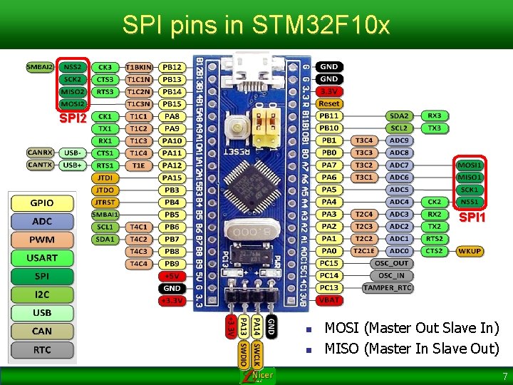
SPI pins in STM 32 F 10 x SPI 2 SPI 1 n n MOSI (Master Out Slave In) MISO (Master In Slave Out) 7

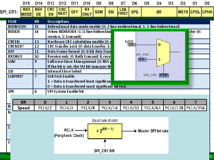
Field BIDIMODE BIDIOE CRCEN CRCNEXT DFF RXONLY SSM SSI LSBFIRST SPE BR BR Speed MSTR CPOL CPHA Bit 15 14 Descriptions Bidirectional data mode enable (0: 2 -line unidirectional, 1: 1 -line bidirectional) When BIDIMODE=1 (1 -line bidirectional), the BIDIOE bit selects the direction of transfer (0: receive, 1: transmit) 13 Hardware CRC calculation enable (0: disabled, 1: enabled) 12 CRC transfer next (0: data transfer, 1: next transfer is CRC) 11 Data Frame format (0: 8 -bit data frame, 1: 16 -bit data frame) 10 Receive only (0: Both transmit & receive (Full-duplex), 1: Receive only) 9 Software Slave Management (0: NSS pin, 1: SSI bit) If the bit is set, the SSI bit manages the communication instead of the NSS pin. 8 Internal Slave Select 7 LSB First Enable 1 = Data is transferred least significant bit first. 0 = Data is transferred most significant bit first. 6 SPI System Enable bit 1 = Enables SPI port and configures pins as serial port pins 0 0 = Disables 1 SPI port and 2 configures 3 these pins as 4 I/O ports 5 6 7 5 -3 PCLK/2 Baud rate control PCLK/4 PCLK/8 PCLK/16 PCLK/32 PCLK/64 PCLK/128 PCLK/256 2 SPI Master/Slave mode Select bit. This bit selects master or slave mode. 1 = SPI in master mode 0 = SPI in slave mode 1 SPI Clock Polarity bit 1 = Active-LOW clocks selected. In idle state SCK is high. 0 = Active-HIGH clocks selected. In idle state SCK is low. 0 SPI Clock Phase bit 1 = Sampling of data occurs at even edges of the SCK clock. 0 = Sampling of data occurs at odd edges of the SCK clock. 8

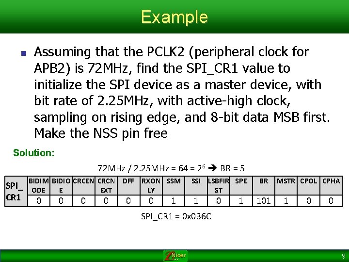
Example n Assuming that the PCLK 2 (peripheral clock for APB 2) is 72 MHz, find the SPI_CR 1 value to initialize the SPI device as a master device, with bit rate of 2. 25 MHz, with active-high clock, sampling on rising edge, and 8 -bit data MSB first. Make the NSS pin free Solution: 72 MHz / 2. 25 MHz = 64 = 26 BR = 5 SPI_ CR 1 BIDIM BIDIO CRCEN CRCN DFF RXON SSM ODE E EXT LY 0 0 0 1 SSI LSBFIR SPE ST 1 0 1 BR 101 MSTR CPOL CPHA 1 0 0 SPI_CR 1 = 0 x 036 C 9

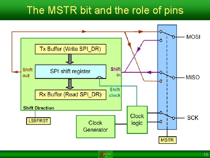
The MSTR bit and the role of pins 10

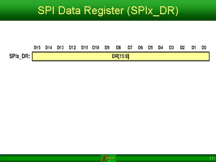
SPI Data Register (SPIx_DR) 11

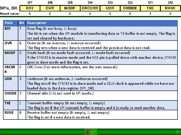
Field BSY OVR MODF CRCER R UDR Bit Description 7 Busy flag (0: not busy, 1: busy) The bit is set when the SPI module is transferring data or TX buffer is not empty. The flag is set and cleared by hardware. 6 Overrun (0: no overrun, 1: overrun occurred) The flag sets when a new data is received and the previous data is not read. 5 Mode fault (0: no mode fault occurred, 1: mode fault occurred) If the STM 32 is in master mode and the NSS pin is pulled down with another device, STM 32 goes to slave mode and the flag is set. 4 CRC Error (For more information, see the user manual. ) 3 CHSIDE 2 TXE 1 RXNE 0 Underrun (0: no underrun, 1: underrun occurred) The flag sets if the STM 32 is in slave mode and a SCLK clock is appeared while we have not loaded data to the data register (SPI_DR). Channel side (It is not used in SPI mode. ) Transmit buffer empty (0: not empty, 1: empty) The flag is set if the SPI transmit buffer is empty and it is ready to send another data. Receive buffer not empty (0: empty, 1: not empty) The flag is set if a new data is received. 12

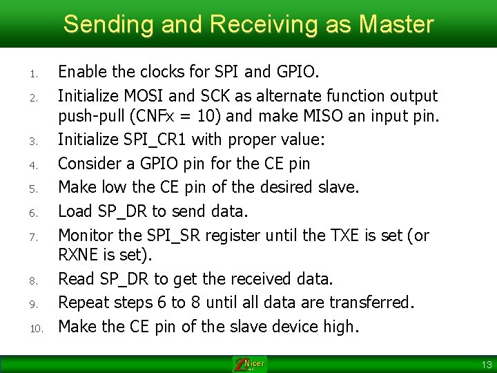
Sending and Receiving as Master 1. 2. 3. 4. 5. 6. 7. 8. 9. 10. Enable the clocks for SPI and GPIO. Initialize MOSI and SCK as alternate function output push-pull (CNFx = 10) and make MISO an input pin. Initialize SPI_CR 1 with proper value: Consider a GPIO pin for the CE pin Make low the CE pin of the desired slave. Load SP_DR to send data. Monitor the SPI_SR register until the TXE is set (or RXNE is set). Read SP_DR to get the received data. Repeat steps 6 to 8 until all data are transferred. Make the CE pin of the slave device high. 13

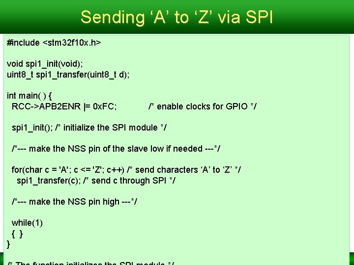
Sending ‘A’ to ‘Z’ via SPI #include <stm 32 f 10 x. h> void spi 1_init(void); uint 8_t spi 1_transfer(uint 8_t d); int main( ) { RCC->APB 2 ENR |= 0 x. FC; /* enable clocks for GPIO */ spi 1_init(); /* initialize the SPI module */ /*--- make the NSS pin of the slave low if needed ---*/ for(char c = 'A'; c <= 'Z'; c++) /* send characters ‘A’ to ‘Z’ */ spi 1_transfer(c); /* send c through SPI */ /*--- make the NSS pin high ---*/ while(1) { } } 14

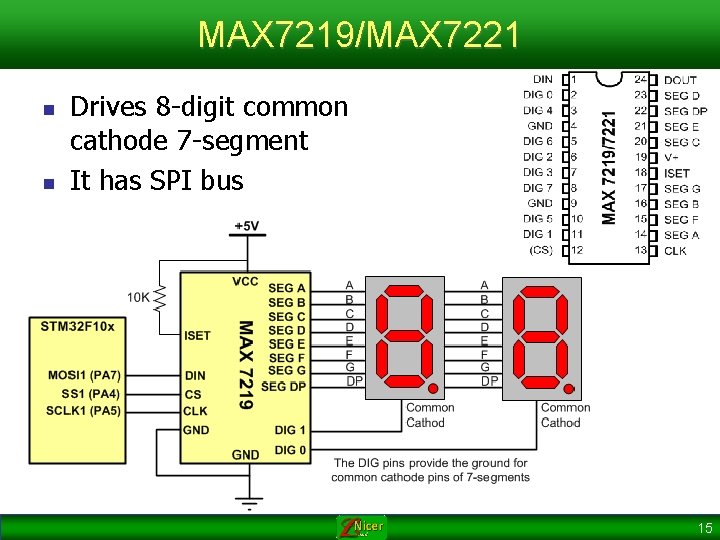
MAX 7219/MAX 7221 n n Drives 8 -digit common cathode 7 -segment It has SPI bus 15

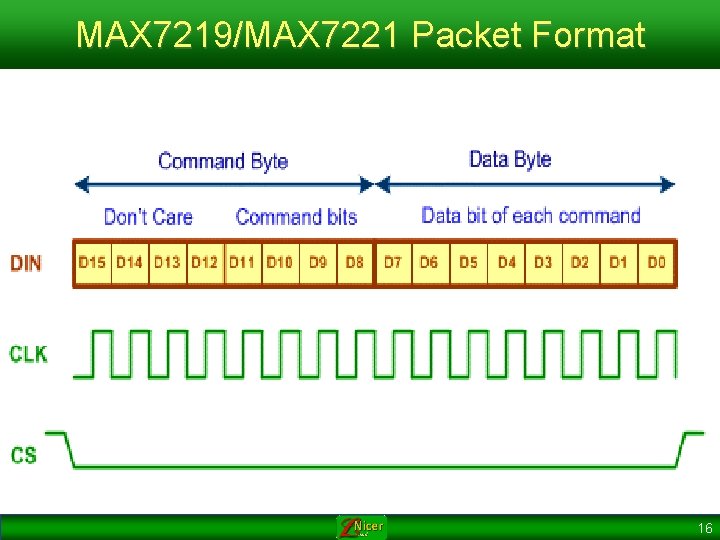
MAX 7219/MAX 7221 Packet Format 16

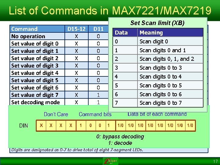
List of Commands in MAX 7221/MAX 7219 Command D 15 -12 No operation X Set value of digit 0 X Set value of digit 1 X Set value of digit 2 X Set value of digit 3 X Set value of digit 4 X Set value of digit 5 X Set value of digit 6 X Set value of digit 7 X Set decoding mode X Set intensity of light X Set scan limit X Turn on/off X Display test X D 11 0 0 0 0 1 1 1 Set Scan limit (XB) D 10 D 9 D 8 Hex Code Data Meaning 0 0 0 X 0 00 0 Scan digit 1 0 X 1 10 1 Scan digits 0 0 and 1 X 2 1 Scan digits 1 0, 1, and X 32 20 0 Scan digits 0 0 to 3 X 4 31 1 0 1 X 5 4 Scan digits 0 to 4 1 1 0 X 6 51 1 Scan digits 1 0 to 5 X 7 60 0 Scan digits 0 0 to 6 X 8 0 Scan digits 1 0 to 7 X 9 70 0 1 0 XA 0 1 1 XB 1 0 0 XC 1 1 1 XF 0: bypass decoding Notes: 1: decode X means don't care. Digits are designated as 0 -7 to drive total of eight 7 -segment LEDs. 17

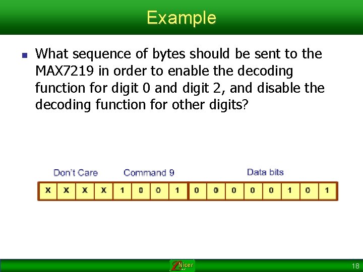
Example n What sequence of bytes should be sent to the MAX 7219 in order to enable the decoding function for digit 0 and digit 2, and disable the decoding function for other digits? 18

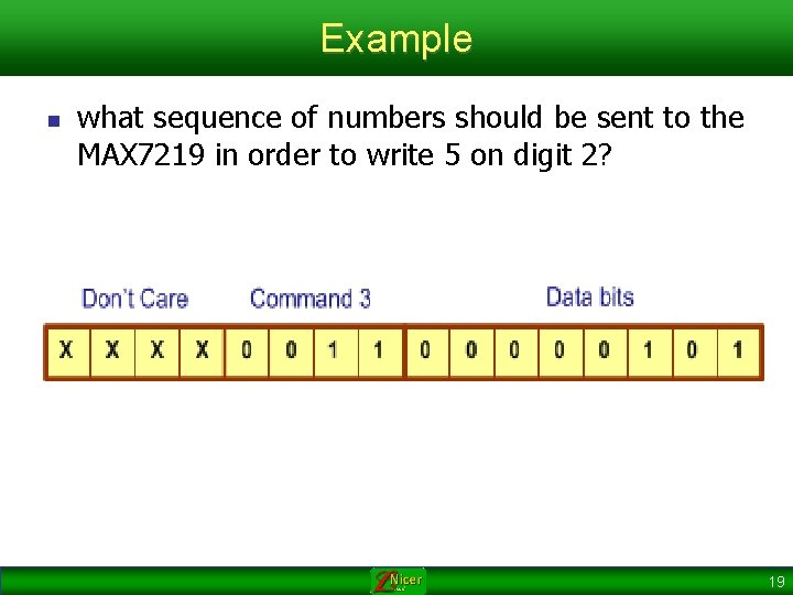
Example n what sequence of numbers should be sent to the MAX 7219 in order to write 5 on digit 2? 19

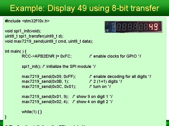
Example: Display 49 using 8 -bit transfer #include <stm 32 f 10 x. h> void spi 1_init(void); uint 8_t spi 1_transfer(uint 8_t d); void max 7219_send(uint 8_t cmd, uint 8_t data); int main( ) { RCC->APB 2 ENR |= 0 x. FC; /* enable clocks for GPIO */ spi 1_init(); /* initialize the SPI module */ max 7219_send(0 x 09, 0 x. FF); max 7219_send(0 x 0 B, 1); max 7219_send(0 x 0 C, 0 x 01); /* enable decoding for all digits */ /* 2 (1+1) digits */ /* turn on */ max 7219_send(0 x 01, 9); /* show 9 on digit 1 */ max 7219_send(0 x 02, 4); /* show 4 on digit 2 */ while(1) { } } 20

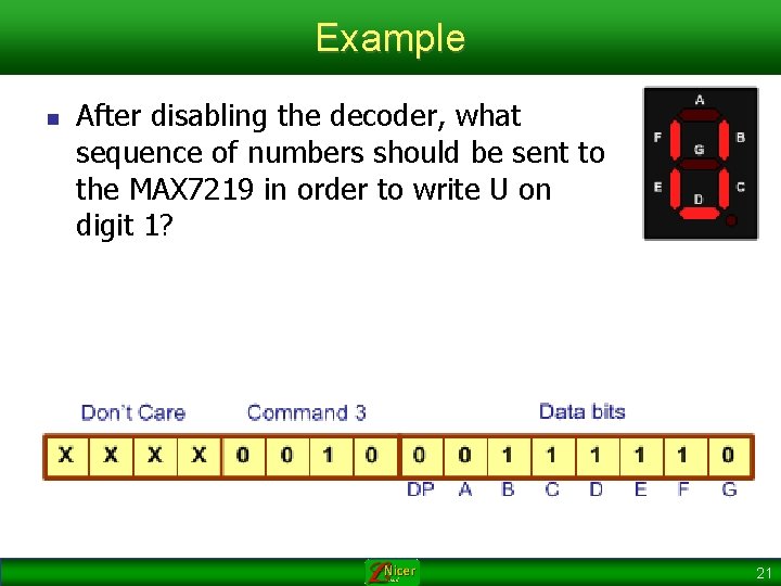
Example n After disabling the decoder, what sequence of numbers should be sent to the MAX 7219 in order to write U on digit 1? 21

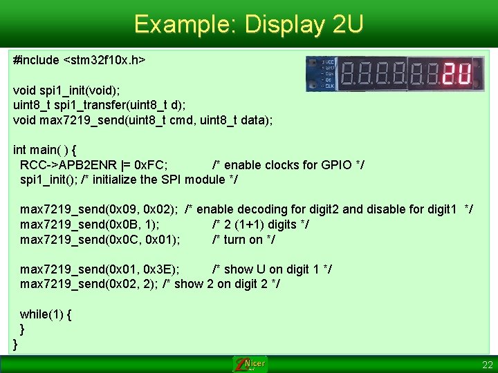
Example: Display 2 U #include <stm 32 f 10 x. h> void spi 1_init(void); uint 8_t spi 1_transfer(uint 8_t d); void max 7219_send(uint 8_t cmd, uint 8_t data); int main( ) { RCC->APB 2 ENR |= 0 x. FC; /* enable clocks for GPIO */ spi 1_init(); /* initialize the SPI module */ max 7219_send(0 x 09, 0 x 02); /* enable decoding for digit 2 and disable for digit 1 */ max 7219_send(0 x 0 B, 1); /* 2 (1+1) digits */ max 7219_send(0 x 0 C, 0 x 01); /* turn on */ max 7219_send(0 x 01, 0 x 3 E); /* show U on digit 1 */ max 7219_send(0 x 02, 2); /* show 2 on digit 2 */ while(1) { } } 22