Speedstack PCB Stack Up Data Exchange Using IPC2581
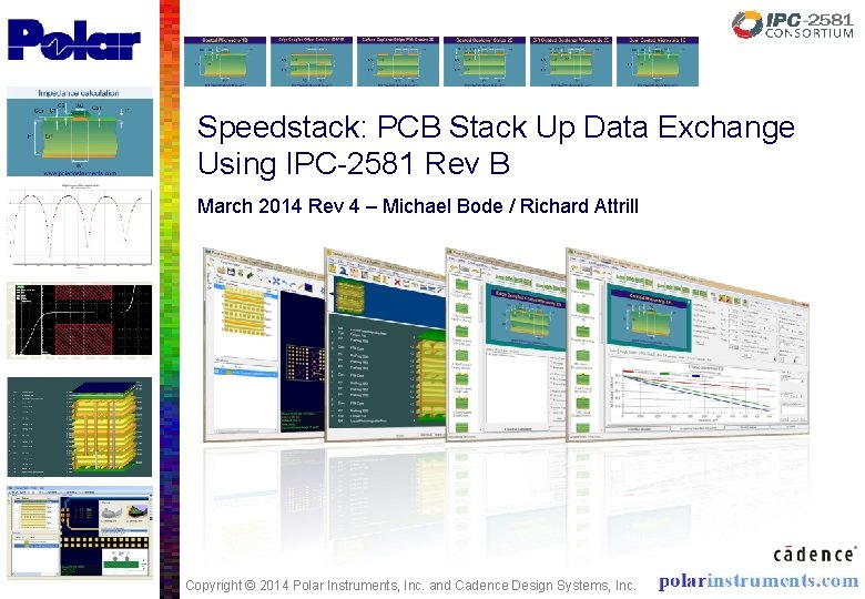
Speedstack: PCB Stack Up Data Exchange Using IPC-2581 Rev B March 2014 Rev 4 – Michael Bode / Richard Attrill Copyright © 2014 Polar Instruments, Inc. and Cadence Design Systems, Inc.
PCB Stack up data exchange using IPC-2581 Introduction to IPC-2581 An efficient data exchange format to be used between designers and manufacturers of printed circuit boards A replacement for the multiple Gerber, NC Drill, Net List, Stack Up and Documentation files normally included within a data set that a designer sends for fabrication and assembly A single file rather than multiple files Uses industry-standard XML format 2 Copyright © 2014 Polar Instruments, Inc. and Cadence Design Systems, Inc.
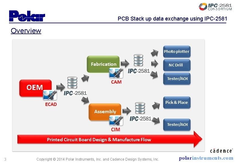
PCB Stack up data exchange using IPC-2581 Overview 3 Copyright © 2014 Polar Instruments, Inc. and Cadence Design Systems, Inc.
PCB Stack up data exchange using IPC-2581 Consortium Members 4 Copyright © 2014 Polar Instruments, Inc. and Cadence Design Systems, Inc.
PCB Stack up data exchange using IPC-2581 Why change from existing data formats? Gerber is a proven format, but it really does not have the intelligence customers need today to communicate design data to manufacturing It lacks stack up details It lacks net list information It lacks other data such as bill of materials and manufacturing notes 5 Copyright © 2014 Polar Instruments, Inc. and Cadence Design Systems, Inc.
PCB Stack up data exchange using IPC-2581 Versions IPC-2581 Original Release – March 2004 (yes, 2004 !) IPC-2581 Rev 1 – May 2007 IPC-2581 Rev A – May 2012 IPC-2581 Rev B – September 2013 Many enhancements introduced with IPC-2581 Rev B including a the ability to comprehensively define the stack up requirement 6 Copyright © 2014 Polar Instruments, Inc. and Cadence Design Systems, Inc.
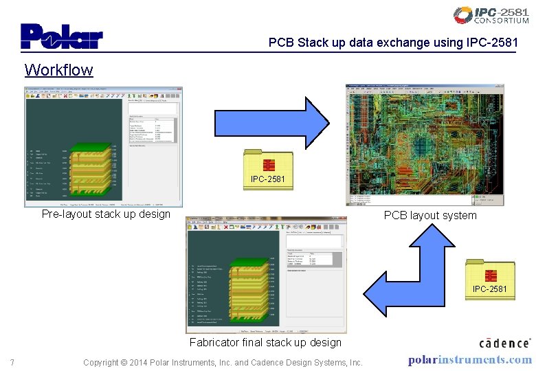
PCB Stack up data exchange using IPC-2581 Workflow IPC-2581 Pre-layout stack up design PCB layout system IPC-2581 Fabricator final stack up design 7 Copyright © 2014 Polar Instruments, Inc. and Cadence Design Systems, Inc.
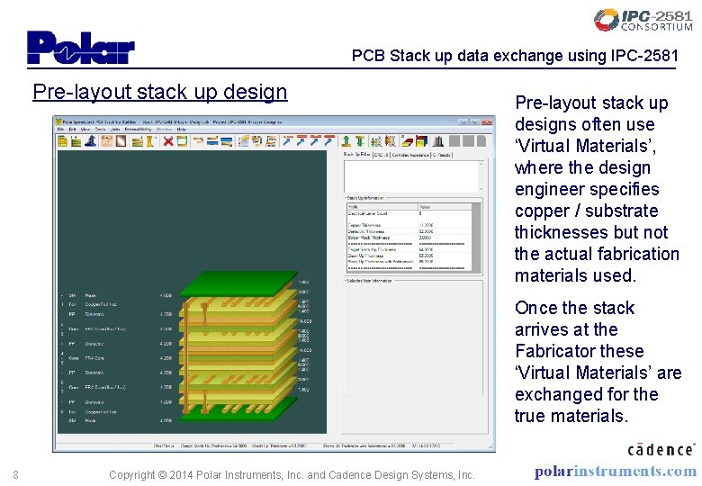
PCB Stack up data exchange using IPC-2581 Pre-layout stack up designs often use ‘Virtual Materials’, where the design engineer specifies copper / substrate thicknesses but not the actual fabrication materials used. Once the stack arrives at the Fabricator these ‘Virtual Materials’ are exchanged for the true materials. 8 Copyright © 2014 Polar Instruments, Inc. and Cadence Design Systems, Inc.
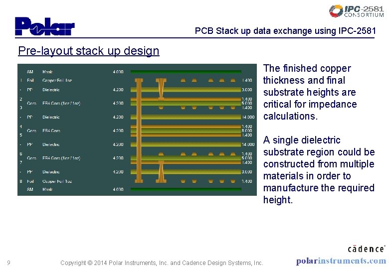
PCB Stack up data exchange using IPC-2581 Pre-layout stack up design The finished copper thickness and final substrate heights are critical for impedance calculations. A single dielectric substrate region could be constructed from multiple materials in order to manufacture the required height. 9 Copyright © 2014 Polar Instruments, Inc. and Cadence Design Systems, Inc.
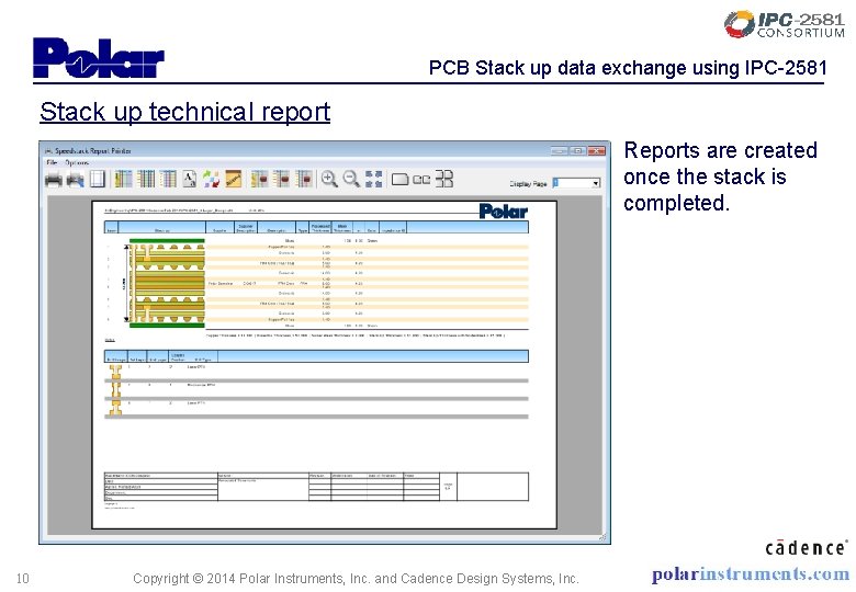
PCB Stack up data exchange using IPC-2581 Stack up technical report Reports are created once the stack is completed. 10 Copyright © 2014 Polar Instruments, Inc. and Cadence Design Systems, Inc.
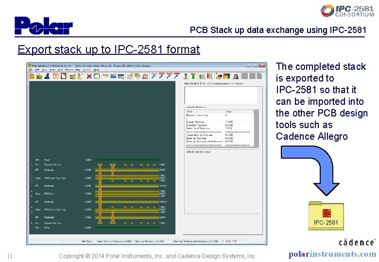
PCB Stack up data exchange using IPC-2581 Export stack up to IPC-2581 format The completed stack is exported to IPC-2581 so that it can be imported into the other PCB design tools such as Cadence Allegro IPC-2581 11 Copyright © 2014 Polar Instruments, Inc. and Cadence Design Systems, Inc.
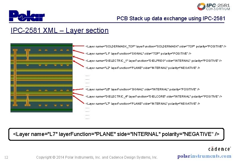
PCB Stack up data exchange using IPC-2581 XML – Layer section <Layer name="SOLDERMASK_TOP" layer. Function="SOLDERMASK" side="TOP" polarity="POSITIVE" /> <Layer name="L 1" layer. Function="SIGNAL" side="TOP" polarity="POSITIVE“ /> <Layer name="DIELECTRIC_1" layer. Function="DIELPREG" side="INTERNAL" polarity="POSITIVE“ /> <Layer name="L 2" layer. Function="PLANE" side="INTERNAL" polarity="NEGATIVE“ /> …. …. <Layer name="L 6" layer. Function=“SIGNAL" side="INTERNAL" polarity=“POSITIVE“ /> <Layer name="DIELECTRIC_4" layer. Function="DIELCORE" side="INTERNAL" polarity="POSITIVE“ /> <Layer name="L 7" layer. Function="PLANE" side="INTERNAL" polarity="NEGATIVE“ /> …. …. <Layer name="L 7" layer. Function="PLANE" side="INTERNAL" polarity="NEGATIVE“ /> 12 Copyright © 2014 Polar Instruments, Inc. and Cadence Design Systems, Inc.
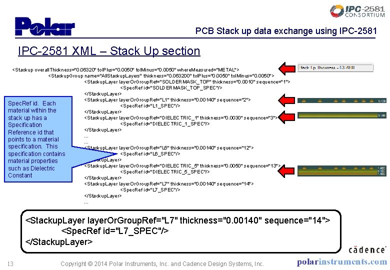
PCB Stack up data exchange using IPC-2581 XML – Stack Up section <Stackup overall. Thickness="0. 06320" tol. Plus="0. 0050" tol. Minus="0. 0050" where. Measured="METAL"> <Stackup. Group name="All. Stackup. Layers" thickness="0. 063200" tol. Plus="0. 0050" tol. Minus="0. 0050"> <Stackup. Layer layer. Or. Group. Ref="SOLDERMASK_TOP" thickness="0. 0010" sequence="1"> <Spec. Ref id="SOLDERMASK_TOP_SPEC"/> </Stackup. Layer> <Stackup. Layer layer. Or. Group. Ref="L 1" thickness="0. 00140" sequence="2"> Spec. Ref id. Each <Spec. Ref id="L 1_SPEC"/> material within the </Stackup. Layer> <Stackup. Layer layer. Or. Group. Ref="DIELECTRIC_1" thickness="0. 0030" sequence="3"> stack up has a <Spec. Ref id="DIELECTRIC_1_SPEC"/> Specification </Stackup. Layer> Reference id that … points to a material … specification. This <Stackup. Layer layer. Or. Group. Ref="L 6" thickness="0. 00140" sequence="12"> <Spec. Ref id="L 6_SPEC"/> specification contains </Stackup. Layer> material properties <Stackup. Layer layer. Or. Group. Ref="DIELECTRIC_5" thickness="0. 0050" sequence="13"> such as Dielectric <Spec. Ref id="DIELECTRIC_5_SPEC"/> Constant </Stackup. Layer> <Stackup. Layer layer. Or. Group. Ref="L 7" thickness="0. 00140" sequence="14"> <Spec. Ref id="L 7_SPEC"/> </Stackup. Layer> … <Stackup. Layer layer. Or. Group. Ref="L 7" thickness="0. 00140" sequence="14"> <Spec. Ref id="L 7_SPEC"/> </Stackup. Layer> 13 Copyright © 2014 Polar Instruments, Inc. and Cadence Design Systems, Inc.
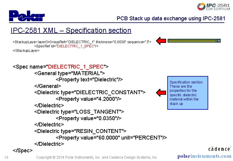
PCB Stack up data exchange using IPC-2581 XML – Specification section <Stackup. Layer layer. Or. Group. Ref="DIELECTRIC_1" thickness="0. 0030" sequence="3"> <Spec. Ref id="DIELECTRIC_1_SPEC"/> </Stackup. Layer> <Spec name="DIELECTRIC_1_SPEC"> <General type="MATERIAL"> <Property text="Dielectric"/> </General> <Dielectric type="DIELECTRIC_CONSTANT"> <Property value="4. 2000"/> </Dielectric> <Dielectric type="LOSS_TANGENT"> <Property value="0. 0350"/> </Dielectric> <Dielectric type="RESIN_CONTENT"> <Property value="60. 0000" unit="PERCENT"/> </Dielectric> </Spec> 14 Copyright © 2014 Polar Instruments, Inc. and Cadence Design Systems, Inc. Specification section. These are the properties for the specific dielectric material within the stack up
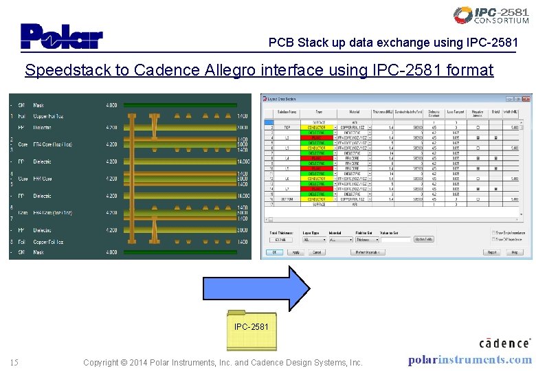
PCB Stack up data exchange using IPC-2581 Speedstack to Cadence Allegro interface using IPC-2581 format IPC-2581 15 Copyright © 2014 Polar Instruments, Inc. and Cadence Design Systems, Inc.
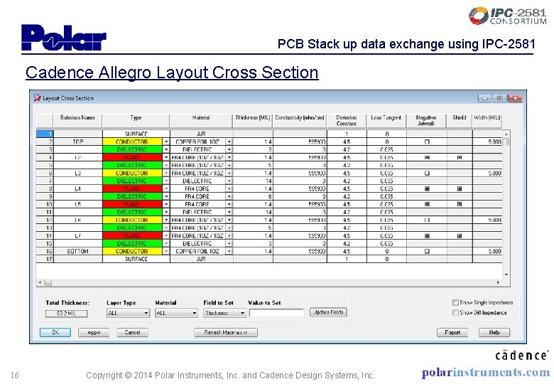
PCB Stack up data exchange using IPC-2581 Cadence Allegro Layout Cross Section 16 Copyright © 2014 Polar Instruments, Inc. and Cadence Design Systems, Inc.
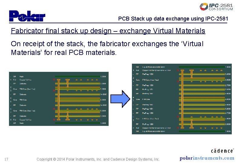
PCB Stack up data exchange using IPC-2581 Fabricator final stack up design – exchange Virtual Materials On receipt of the stack, the fabricator exchanges the ‘Virtual Materials’ for real PCB materials. 17 Copyright © 2014 Polar Instruments, Inc. and Cadence Design Systems, Inc.
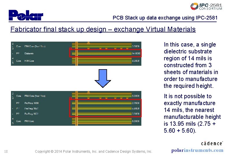
PCB Stack up data exchange using IPC-2581 Fabricator final stack up design – exchange Virtual Materials In this case, a single dielectric substrate region of 14 mils is constructed from 3 sheets of materials in order to manufacture the required height. It is not possible to exactly manufacture 14 mils, the nearest manufacturable height is 13. 95 mils (2. 75 + 5. 60). 18 Copyright © 2014 Polar Instruments, Inc. and Cadence Design Systems, Inc.
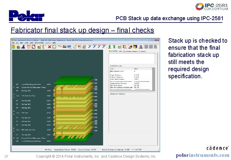
PCB Stack up data exchange using IPC-2581 Fabricator final stack up design – final checks Stack up is checked to ensure that the final fabrication stack up still meets the required design specification. 19 Copyright © 2014 Polar Instruments, Inc. and Cadence Design Systems, Inc.
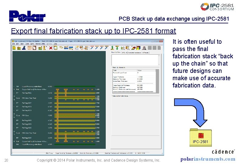
PCB Stack up data exchange using IPC-2581 Export final fabrication stack up to IPC-2581 format It is often useful to pass the final fabrication stack “back up the chain” so that future designs can make use of accurate fabrication data. IPC-2581 20 Copyright © 2014 Polar Instruments, Inc. and Cadence Design Systems, Inc.
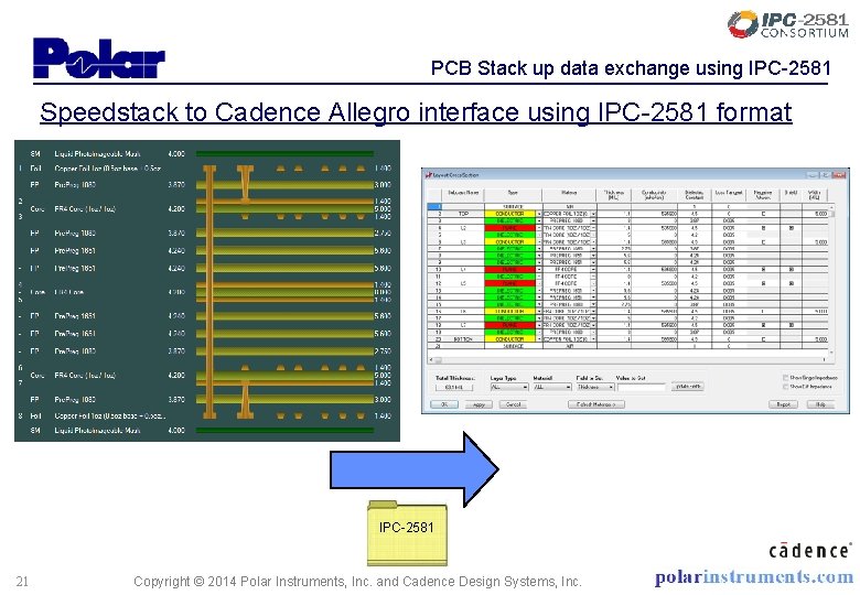
PCB Stack up data exchange using IPC-2581 Speedstack to Cadence Allegro interface using IPC-2581 format IPC-2581 21 Copyright © 2014 Polar Instruments, Inc. and Cadence Design Systems, Inc.
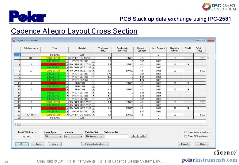
PCB Stack up data exchange using IPC-2581 Cadence Allegro Layout Cross Section 22 Copyright © 2014 Polar Instruments, Inc. and Cadence Design Systems, Inc.
PCB Stack up data exchange using IPC-2581 Summary of using IPC-2581 format for stack up data exchange A comprehensive, single file data format Allows for the exchange of data between designers and fabricators Supported by a growing consortium of software vendors and users Polar will be releasing a version of Speedstack with export to IPC 2581 capability at the end of March, 2014. For more information: www. ipc 2581. com 23 Copyright © 2014 Polar Instruments, Inc. and Cadence Design Systems, Inc.
Thank you Copyright © 2014 Polar Instruments, Inc. and Cadence Design Systems, Inc.
- Slides: 24