Special Purpose Programmable Peripheral Devices and Their Interfacing
Special Purpose Programmable Peripheral Devices and Their Interfacing 1
PROGRAMMABLE INTERVAL TIMER (8253) • Intel’s programmable counter/timer device (8253) facilitates the generation of accurate time delays. • When 8253 is used as a timing and delay generation peripheral, the microprocessor becomes free from the task related to the counting process and can execute the programs in memory, while the timer device may perform the counting tasks. • This minimizes the software overhead on the microprocessor. 2
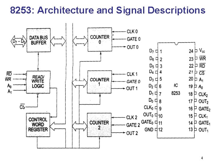
8253: Architecture and Signal Descriptions • The programmable timer device 8253 contains three independent 16 bit counters, each with maximum count rate of 2. 6 MHz it is thus possible to generate three totally independent delays or maintain three independent counters simultaneously. • All the three counters may be independently controlled by programming the three internal command word registers. • The 8 bit, bidirectional data buffer interfaces internal circuit of 8253 to microprocessor system bus. • The internal block diagram and pin diagram of 8253 are shown in figures. 3
8253: Architecture and Signal Descriptions 4
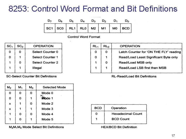
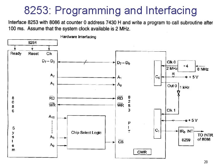
8253: Architecture and Signal Descriptions • A 0, A 1 pins are the address input pins and are required internally for addressing the mode control word registers and the three counter registers. A low on ‘CS bar’ line enables the 8253. No operation will be performed by 8253 till it is enabled. • The 8253 can operate in any one of the six different modes. A control word must be written in the respective control word register by the micro processor to initialize each of the counters of 8253 to decide operating mode. 5
8253: Operating Modes • Each of three counters of 8253 can be operated in one of the following six modes of operation: – Mode 0 (Interrupt on terminal count) – Mode 1 (Programmable monoshot) – Mode 2 (Rate generator) – Mode 3 (square wave generator) – Mode 4(Software triggered strobe) – Mode 5 (Hardware triggered strobe) 6
8253: Operating Modes • MODE 0 – This mode of operation is generally called as interrupt on terminal count. – In this mode the output is initially low after the mode is set. – The output remains low even after the count value is loaded in the counter. – The counter starts decrementing the count value after the falling edge of the clock, if the GATE input is high. – The process of decrementing the counter continues at each falling edge of the clock till the terminal count is reached. 7
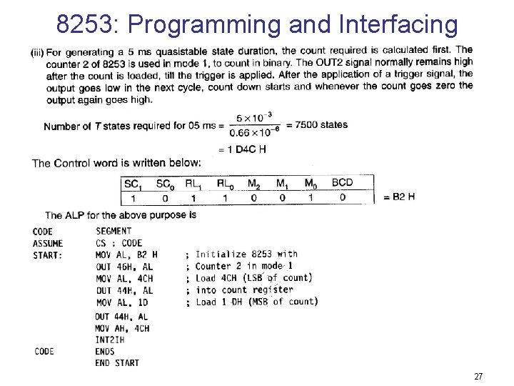
8253: Operating Modes • MODE 1 – This mode of operation of 8253 is called programmable one shot mode. – As the name implies, in this mode, 8253 can be used as mono-stable multivibrator. – The duration of the quasistable state of the mono-stable multivibrator is decided by the count loaded in the count register. – The gate input is used as trigger input in this mode of operation. – Normally the output remains high till the suitable count loaded in the count register and a trigger is applied. – After the application of trigger (on the positive edge), the output goes low and remains low till the count becomes zero. 8
8253: Operating Modes • MODE 2 – This mode is called either rate generator or divide by N counter. – In this mode, if N is loaded as the count value, then, after N pulses, the output becomes low only for one clock cycle. – The count N is reloaded and again the output becomes high and remains so for N clock pulses. – The output is normally high after initialization or even a low signal on GATE input can force the output to go high. – If GATE goes high, the counter starts counting down from the initial value. – The counter generates an active low pulse at the output initially, after the count register is loaded with a count value. – Then countdown starts and whenever the count becomes zero another active low pulse is generated at the output. 9
8253: Operating Modes • MODE 3 – In this mode, the 8253 can be used as a square wave rate generator. – In terms of operation this mode is some what similar to mode 2. – When, the count N loaded is even, then for half of the count, the output remains high and for the remaining half it remains low. – If the count loaded is odd, the first clock pulse decrements it by 1 resulting in an even count value (holding the output high). – Then the output remains high for half of the new count and goes low for the remaining half. – This procedure is repeated continuously resulting in the generation of a square wave. 10
8253: Operating Modes • MODE 4 – This mode of operation of 8253 is named as Software triggered strobe. – After the mode is set, the output goes high. – When a count loaded, counting down starts. – On terminal count, the output goes low for one clock cycle, and then it again goes high. 11
8253: Operating Modes • MODE 5 – This mode of operation also generates a strobe in response to the rising edge at the trigger input. – This mode may be used to generate a delayed strobe in response to an externally generated signal. – Once this mode is programmed and the counter is loaded, the output goes high. – The counter starts counting after the rising edge of the trigger input (GATE). 12
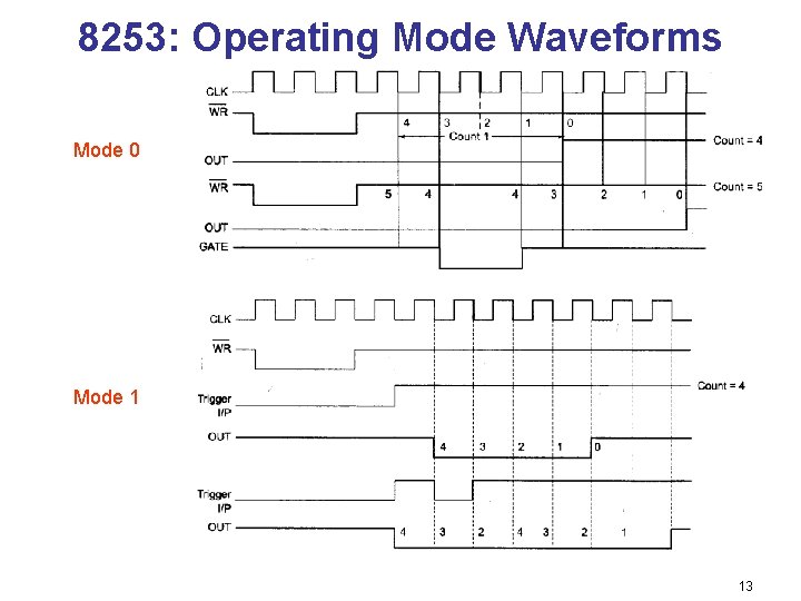
8253: Operating Mode Waveforms Mode 0 Mode 1 13
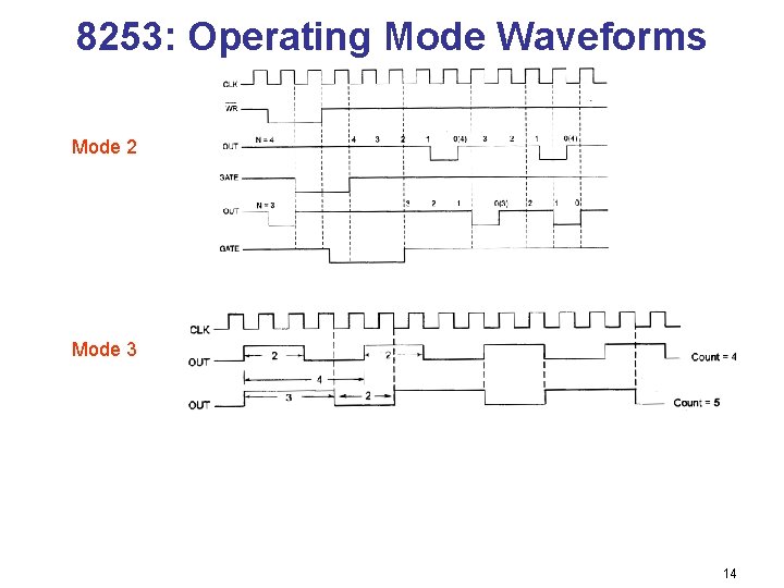
8253: Operating Mode Waveforms Mode 2 Mode 3 14
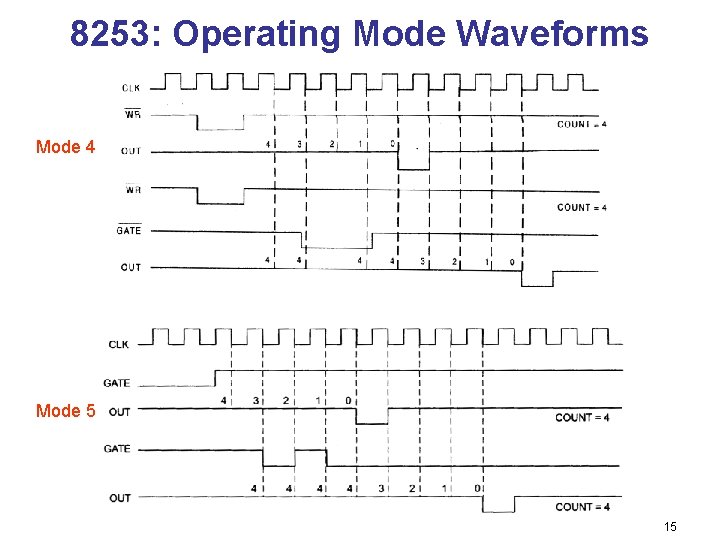
8253: Operating Mode Waveforms Mode 4 Mode 5 15
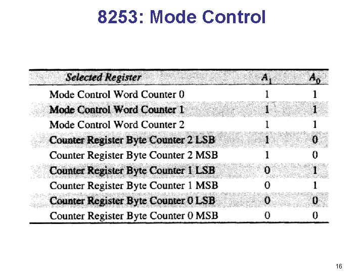
8253: Mode Control 16
8253: Control Word Format and Bit Definitions 17
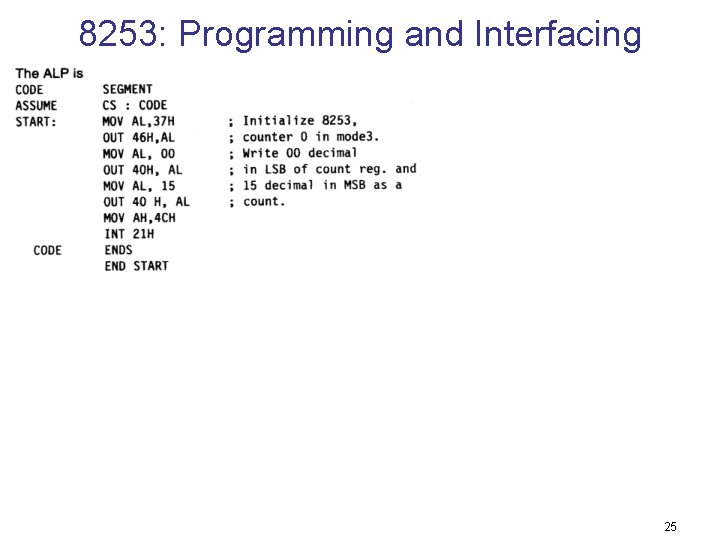
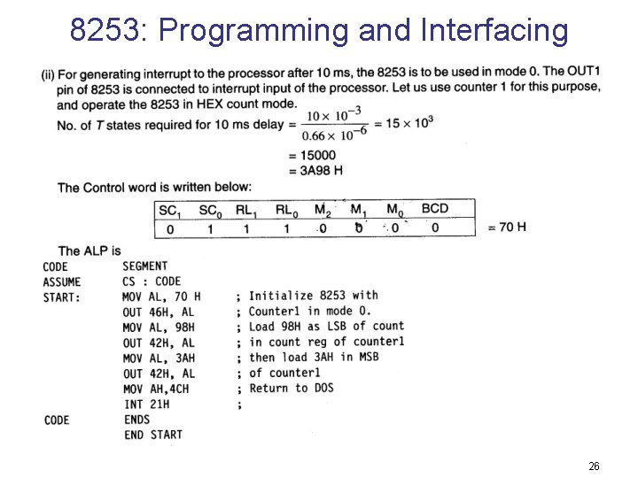
8253: Programming and Interfacing • As it evident from the previous discussion, there may be two types of write operations in 8253, viz. • (i) writing a control word into a control word register and • (ii) writing a count value into a count register. • The control word register, accepts data from the data buffer and initializes the counters, as required. • The control word register contents are used for • • (a) initializing the operating modes (mode 0 – mode 4) (b) selection of counters (counter 0 – counter 2) (c) choosing binary / BCD counters (d) loading of the counter registers. • The mode control register is a write only register and the CPU cannot read its contents. 18
8253: Programming and Interfacing • All the counters in 8253 are down counters, hence their count values go on decrementing if the CLK input pin is applied with a valid clock signal. • A maximum count is obtained by loading all zeroes into a count register, i. e. 2^16 for binary counting and 10^4 for BCD counting. • The 8253 responds to the negative clock edge of the clock input. • The maximum operating clock frequency of 8253 is 2. 6 MHz. • For higher frequencies one can use timer 8254, which operates up to 10 MHz, maintain pin compatibility with 8253. 19
8253: Programming and Interfacing • There are 2 methods for reading 8253 counter registers. – In the first method, either the clock or the counting procedure (using GATE) is inhibited to ensure a stable count. – Then the contents are read by selecting the suitable counter using A 0, A 1 and executing using IN instructions. – The first IN instruction reads the least significant byte and the second IN instruction reads the most significant byte. – In the second method of reading a counter, the counter can be read while counting is in progress. – This method, as already mentioned is called as reading on fly. – In this method, neither clock nor the counting needs to be inhibited to read the counter. 20
8253: Programming and Interfacing • In all the above programs, the counting down starts as soon as the writing operation to the count register is over, and the WR bar pin goes high after writing. • The processor 8085 had five hardware interrupt pins. • Out of these five interrupt pins, four pins were allotted fixed vector addresses but the pin INTR was not allotted any vector address, rather an external device was supposed to hand over the type of the interrupt, i. e. (Type o to 7 for RST 0 to RST 7), to the microprocessor. 21
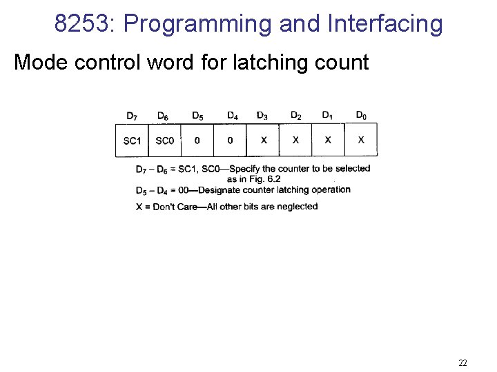
8253: Programming and Interfacing Mode control word for latching count 22
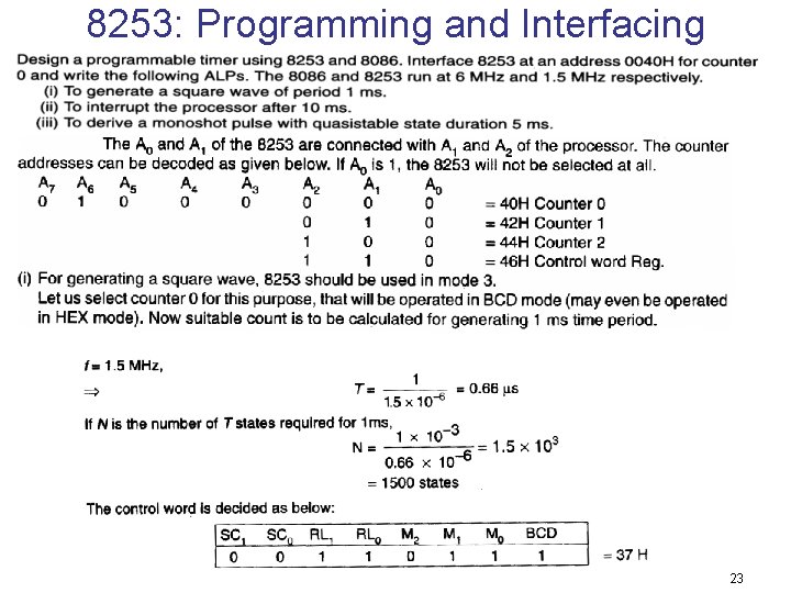
8253: Programming and Interfacing 23
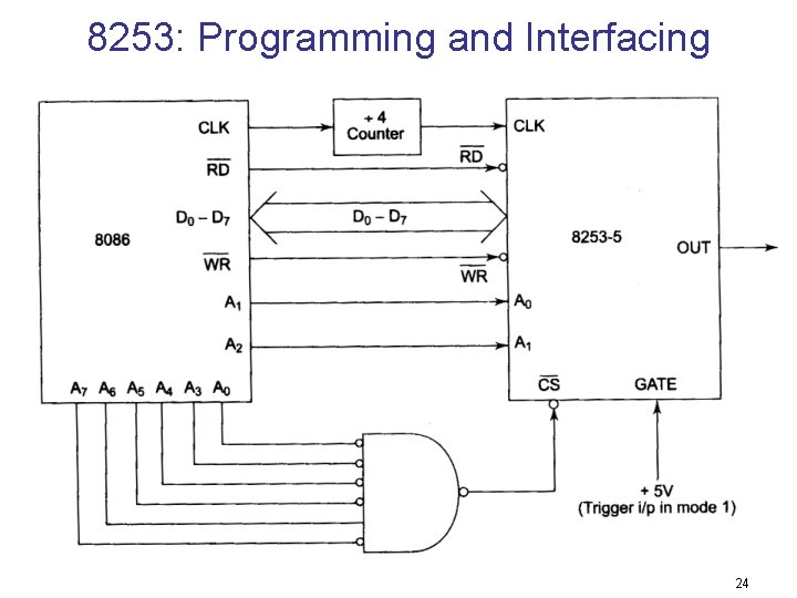
8253: Programming and Interfacing 24
8253: Programming and Interfacing 25
8253: Programming and Interfacing 26
8253: Programming and Interfacing 27
8253: Programming and Interfacing 28
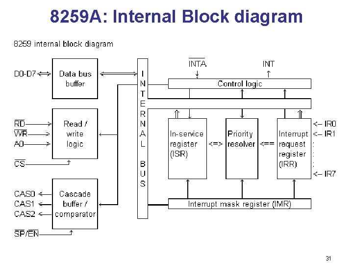
Programmable Interrupt Controller 8259 A • Architecture and Signal Descriptions of 8259 A – Interrupt Request Register (IRR) the interrupts at IRQ input lines are handled by Interrupt Request Register internally. IRR stores all the interrupt requests in it in order to serve them one by one on the priority basis. – IN – Service register (ISR) this stores all the interrupts requests those are being served, i. e. ISR keeps a track of the requests being served. – Priority Resolver this unit determines the priorities of the interrupt requests appearing simultaneously. The highest priority selected and stored Into the corresponding bit of ISR during INTA bar pulse. The IR 0 has the highest priority while the IR 7 has the lowest one, normally in fixed priority mode. The priorities however may be altered by programming the 8259 A in rotating priority mode. 29
8259 A: Pin Configuration 30
8259 A: Internal Block diagram 31
8259 A: Architecture and Signal Descriptions • Interrupt Mask Register (IMR) this register stores the bits required to mask the interrupts inputs. IMR operates on IRR at the direction of the priority resolver. • Interrupt Control Logic this block manages the interrupt and the interrupt acknowledge signals to be sent to the CPU for serving one of the eight interrupt requests. • Data Bus Buffer this tristate bidirectional buffer interfaces internal 8259 A bus to the microprocessor system data bus. Control words, status and vector information pass through data buffer during read or write operations. • Read /write control logic this circuit accepts and decode commands from the CPU. This block also allow the status of the 8259 A to be transferred on to the data bus. 32
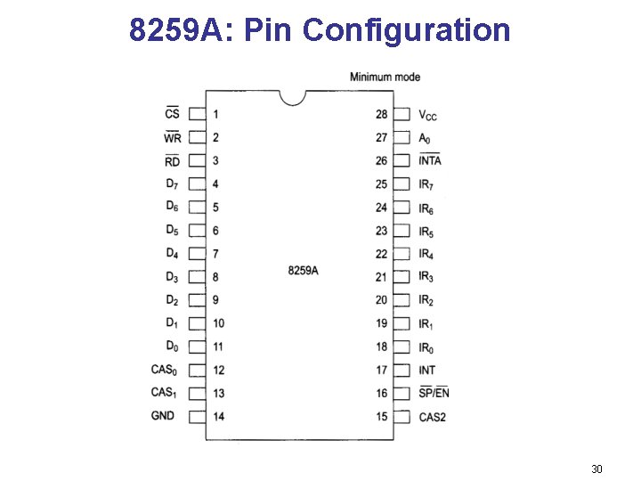
8259 A: Architecture and Signal Descriptions • Cascade Buffer/Comparator this block stores and compares the IDs of all the 8259 A used in the system. The three I/O pins CAS 0 -2 are outputs when the 8259 A is used as master. The same pins act as inputs when the 8259 A is in the slave mode. The 8259 A in the master mode, sends the ID of the interrupting slave device on these lines. The slave thus selected, will send its preprogrammed vector address on the data bus during the next INTA bar pulse. • CS this is an active low chip select signal for enabling RD bar and WR bar operations of 8259 A. INTA bar function is independent of CS bar. • WR bar this pin is an active low enable write input ti 8259 A. this enables it to accept command words from CPU. • RD bar this is an active low read enable input to 8259 A. a low on this line enables 8259 A to release status onto the data bus of CPU. • D 7 – D 0 these pins form a bidirectional data bus that carries 8 bit data either to control word or from status word registers. This also carries interrupt vector information. 33
8259 A: Architecture and Signal Descriptions • CAS 0 – CAS 2 cascade lines a single 8259 A provides eight vectored interrupts. If more interrupts are required, the 8259 A is used in the cascade mode in which a master 8259 A along with eight slaves 8259 A can provide up to 64 vectored interrupts lines. These three lines act as select lines for addressing the slaves 8259 A. • PS bar/ EN bar this pin is a dual purpose pin. When the chip is used in buffered mode, it can be used as a buffer enable to control transreceivers. • INT this pin goes high whenever a valid interrupt request is asserted. This is used to interrupt the CPU and is connected to the interrupt input of CPU. • IR 0 – IR 7 (Interrupts requests) these pins act as input to accept interrupts requests to the CPU. In the edge triggered mode, an interrupt service is requested by raising an IR pin from a low to high state. It is held high until it is acknowledged, and just by latching it to high level, if used in the level triggered mode. 34
8259 A: Architecture and Signal Descriptions • INTA bar: this pin is an input used to strobe – in 8259 A interrupt vector data on to the data bus. In conjunction with CS bar, WR bar, and RD bar pins, this selects the different operations like, writing command words, reading status words, etc. • The device 8259 A can be interfaced with any CPU using either polling or interrupt. In polling, the CPU keeps on checking each peripheral device in sequence to ascertain if it is requires any service from the CPU. If any such service request noticed, the CPU serves the request and then goes on to the next device in sequence. After the peripheral devices are scanned as above the CPU again starts from the first device. • In the interrupt driven method, the CPU performs the main processing task till it is interrupted by a service requesting peripheral device. 35
8259 A: Architecture and Signal Descriptions • The interrupt sequence in an 8086 – 8259 A system is described as follows • One or more IR lines are raised high that set corresponding IRR bits. • 8259 A resolves priority and sends an INT signal to CPU. • the CPU acknowledges with INTA bar pulse • Upon receiving an INTA bar signal from the CPU, the highest priority ISR bit is set and the corresponding IRR bit is reset. The 8259 A does not drive data bus during this period. • The 8086 will initiate a second INTA bar pulse. • This completes the interrupt cycle. The ISR bit is reset at the end of the second INTA bar pulse is automatic end of interrupt (AEOI) mode is programmed. Otherwise ISR bit remains set until an appropriate EOI command is issued at the end of interrupt subroutine. 36
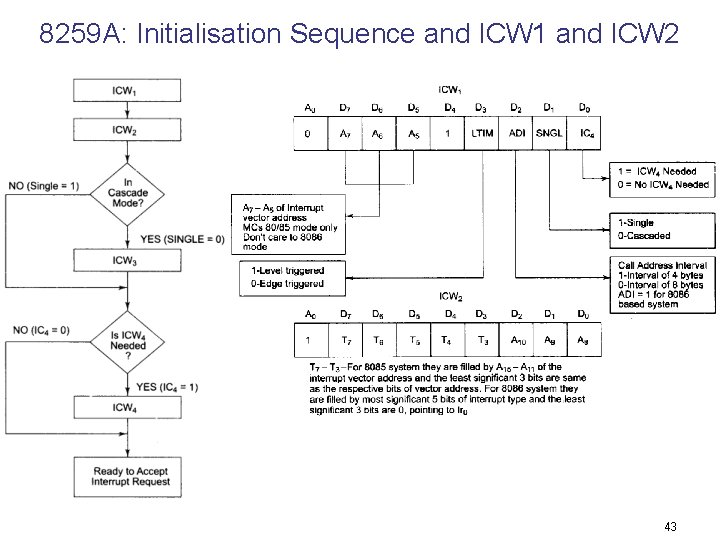
8259 A: Command Words • The command words of 8259 A are classified in two groups, – Initialization command words (ICWs) and – Operation command words (OCWs) • Initialization command words (ICWs) – Before it starts functioning, the 8259 A must be initialized by writing two to four command words in to the respective command word registers. These are called initialization command words (ICWs). – If A 0 = 0 and D 4 =1, the control word recognized as ICW 1. If A 0 = 1, the control word recognized as ICW 2. 37
8259 A: Command Words • Once ICW 1 is loaded, the following initialization procedure is carried out internally. 1. the edge sense circuit is reset, i. e. by default 8259 interrupts are edge sensitive. 2. IMR is cleared 3. IR 7 input is assigned the lowest priority 4. Slave mode address is set to 7 5. Special mask mode is cleared and the status read is set to IRR 6. If IC 4 =0, all the functions of ICW 4 are set to zero. Master/slave bit ICW 4 is used in the buffered mode only. 38
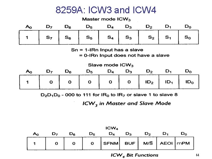
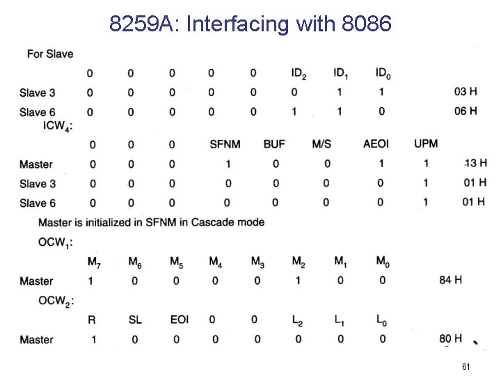
8259 A: Command Words • In the master mode (i. e. SP bar =1 or in buffer mode M/S =1 in ICW 4), the 8 bit slave register will be set bit – wise to ‘ 1’ for each slave in the system, as shown in the fig 6. 16. The requesting slave twill then release the second byte of CALL sequence. • In the slave mode (i. e. SP bar =0 or in buffer mode M/S =0 in ICW 4) bits D 2 to D 0 identify the slave, i. e. 000 to 111 for slave 1 to slave 8. the slaves com[pares the cascade inputs with these bits and if they are equal, the second byte of the CALL sequence is released by it on the data bus. 39
8259 A: Command Words • ICW 4 the use of this command word depends on the IC 4 bit of ICW 1. if IC 4 =1, ICW 4 is used, otherwise it is neglected. The bit functions of ICW 4 are described as follows • SFNM special fully nested mode is selected, if SFNM =1 • BUF if BUF =1, the buffered mode is selected. In the buffered mode, SP/EN acts as enable output and the master/slave is determined using the M/S bit of ICW 4. • M/s if M/S =1. 8259 A is a master. if M/S =0, 8259 A is a slave. If BUF =0, M/S is to be neglected. • AEOI if AEOI=1, the automatic end of interrupt mode is selected. • m. PM if the m. PM bit is 0, Mcs system operation is selected and if m. PM =1, 8086/88 0 eration is selected. 40
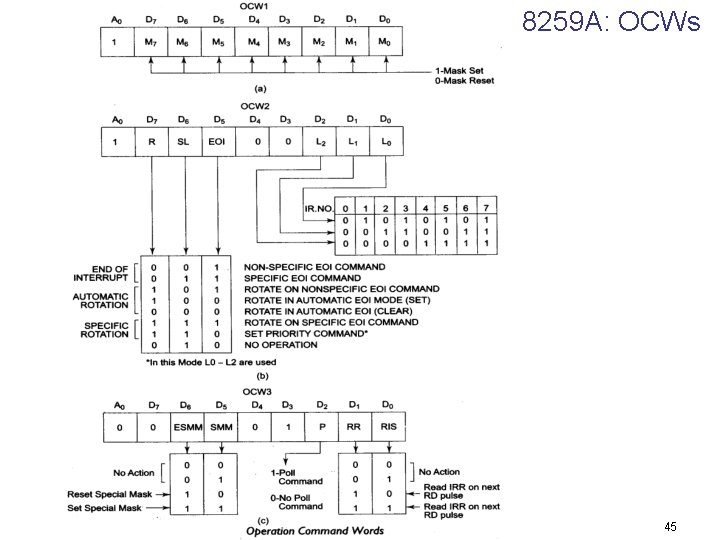
8259 A: Command Words • Operation Command Words – Once 8259 A is initialized using the previously discussed command words for initialization, it is ready for its normal function, i. e. for accepting the interrupts but 8259 A has its own ways of handling the received interrupts called as modes of operation. – These modes of operations can be selected by programming, i. e. writing three internal registers called as operation command word registers. – The data written into them (bit pattern) is called as operation command words. In the three operation command words OCW 1, OCW 2 and OCW 3, every bit corresponds to some operational features of the mode selected, except for a few bits those are either ‘ 1’ or ‘ 0’. OCW 1 is used to mask the unwanted interrupt requests. 41
8259 A: Command Words • Operation Command Words (Continued. . ) – If the mask bit is 1, the corresponding interrupt request is masked, and if it is 0 the request is enabled. In OCW 2 the three bits, viz. R, SL and EOI control the end of interrupt, the rotate mode and their combinations as shown in figure. – The three bits L 2, L 1 and L 0 in OCW 2 determine the interrupt level to be selected for operation, if the SL bit is active, I. e. , 1. – The operation command word 3 (OCW 3), if the ESMM bit, i. e. enable special Mask mode bit is set to ‘ 1’, the SMM bit is enabled to select or mask the special Mask mode. – When the ESMM bit is ‘ 0’, the SMM bit is neglected. If the SMM bit, i. e. special Mask mode bit is ‘ 1’, the 8259 A will enter special Mask mode provided ESMM =1. 42
8259 A: Initialisation Sequence and ICW 1 and ICW 2 43
8259 A: ICW 3 and ICW 4 44
8259 A: OCWs 45
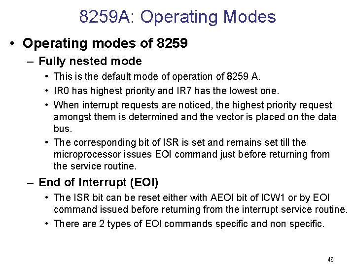
8259 A: Operating Modes • Operating modes of 8259 – Fully nested mode • This is the default mode of operation of 8259 A. • IR 0 has highest priority and IR 7 has the lowest one. • When interrupt requests are noticed, the highest priority request amongst them is determined and the vector is placed on the data bus. • The corresponding bit of ISR is set and remains set till the microprocessor issues EOI command just before returning from the service routine. – End of Interrupt (EOI) • The ISR bit can be reset either with AEOI bit of ICW 1 or by EOI command issued before returning from the interrupt service routine. • There are 2 types of EOI commands specific and non specific. 46
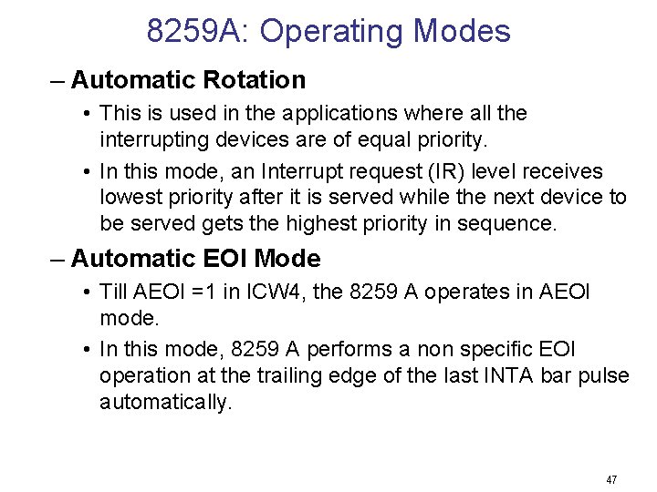
8259 A: Operating Modes – Automatic Rotation • This is used in the applications where all the interrupting devices are of equal priority. • In this mode, an Interrupt request (IR) level receives lowest priority after it is served while the next device to be served gets the highest priority in sequence. – Automatic EOI Mode • Till AEOI =1 in ICW 4, the 8259 A operates in AEOI mode. • In this mode, 8259 A performs a non specific EOI operation at the trailing edge of the last INTA bar pulse automatically. 47
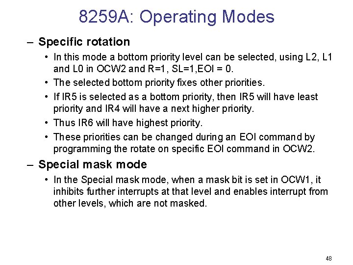
8259 A: Operating Modes – Specific rotation • In this mode a bottom priority level can be selected, using L 2, L 1 and L 0 in OCW 2 and R=1, SL=1, EOI = 0. • The selected bottom priority fixes other priorities. • If IR 5 is selected as a bottom priority, then IR 5 will have least priority and IR 4 will have a next higher priority. • Thus IR 6 will have highest priority. • These priorities can be changed during an EOI command by programming the rotate on specific EOI command in OCW 2. – Special mask mode • In the Special mask mode, when a mask bit is set in OCW 1, it inhibits further interrupts at that level and enables interrupt from other levels, which are not masked. 48
8259 A: Operating Modes – Edge and Level Triggered mode • This mode decides whether the interrupt should be edge triggered or level triggered. • If bit LTIM of ICW 1 = 0, they are edge triggered, otherwise the interrupts are level. – Reading 8259 status • The status of internal registers of 8259 can be read using this mode. • The OCW 3 is used to read IRR and ISR while OCW 1 is used to read IMR. • Reading is possible only in no polled mode. – Poll command • In the poll mode of operation, the INT output of 8259 A is neglected, through it functions normally, by not connecting INT output or by masking INT input of the microprocessor. • The poll mode is entered by setting P =1 in OCW 3. The 8259 A is polled by using software execution by micro processor instead of the requests on INT input. 49
8259 A: Operating Modes – Special fully nested mode • This mode is used more complicated systems, where cascading is used and the priority has to be programmed in the master using ICW 4. • In this mode, when an interrupt request from a certain slave in service, this slave can further send requests to the master, if the requesting device is connected to the slave has higher priority than one being currently served. – Buffered mode • When the 8259 A is used in the systems in which bus driving buffers are used on data busses (e. g. cascaded systems), the problem of enabling the buffers arises. • The 8259 A sends a buffer enable signal on SP bar/EN bar pin, whenever data is placed on the bus. 50
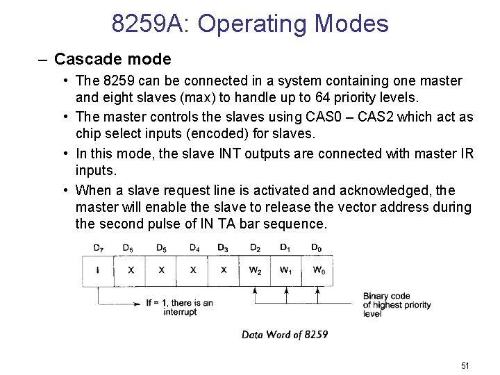
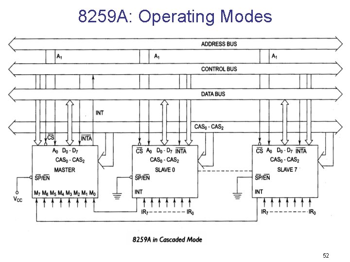
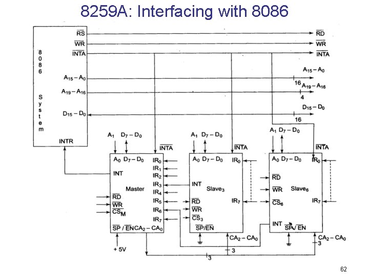
8259 A: Operating Modes – Cascade mode • The 8259 can be connected in a system containing one master and eight slaves (max) to handle up to 64 priority levels. • The master controls the slaves using CAS 0 – CAS 2 which act as chip select inputs (encoded) for slaves. • In this mode, the slave INT outputs are connected with master IR inputs. • When a slave request line is activated and acknowledged, the master will enable the slave to release the vector address during the second pulse of IN TA bar sequence. 51
8259 A: Operating Modes 52
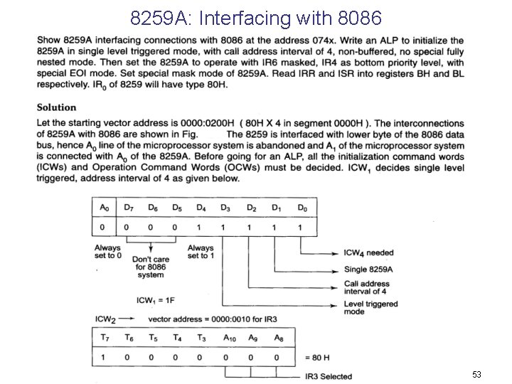
8259 A: Interfacing with 8086 53
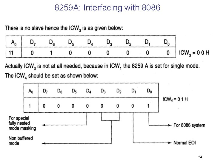
8259 A: Interfacing with 8086 54
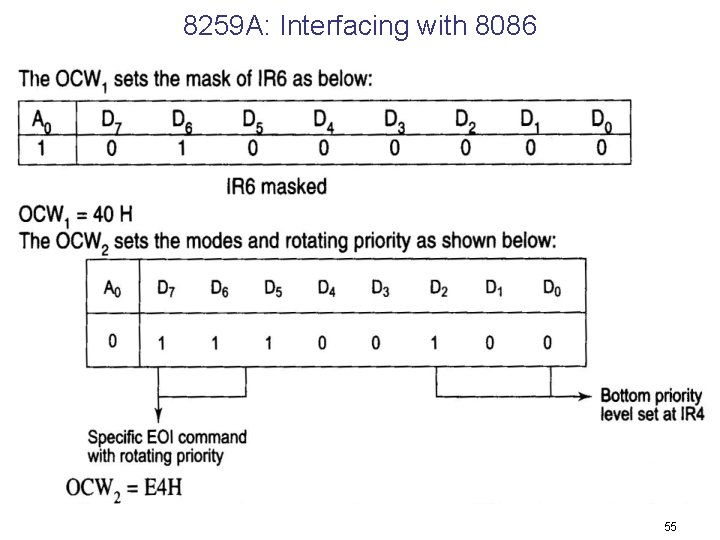
8259 A: Interfacing with 8086 55
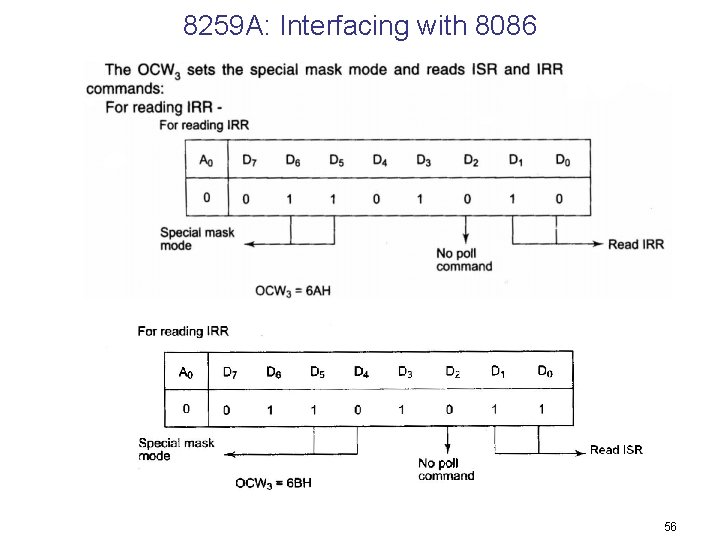
8259 A: Interfacing with 8086 56
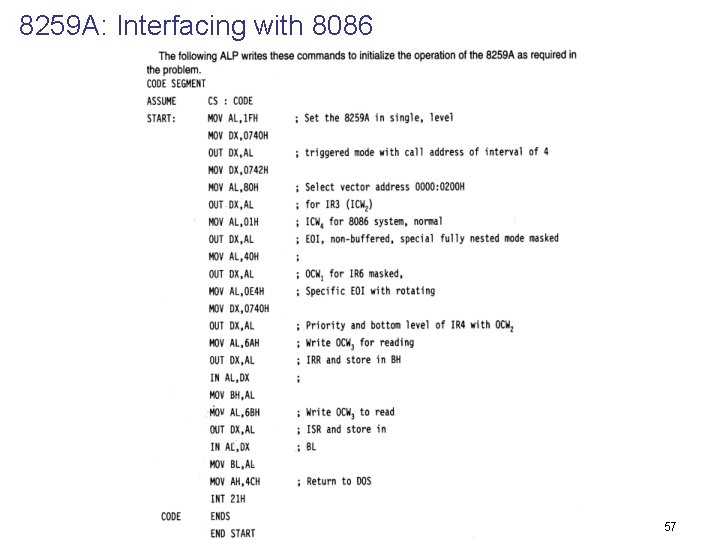
8259 A: Interfacing with 8086 57
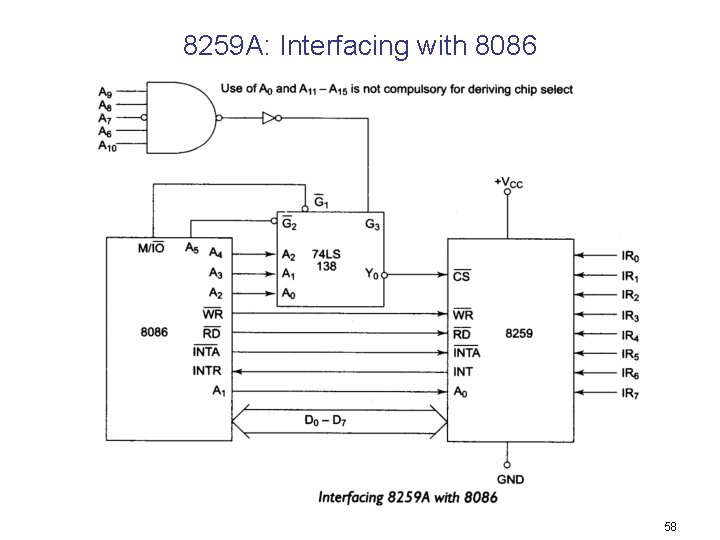
8259 A: Interfacing with 8086 58
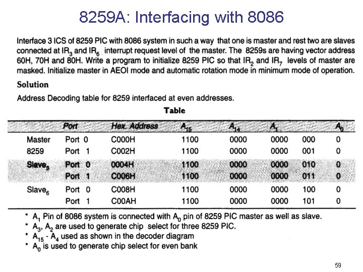
8259 A: Interfacing with 8086 59
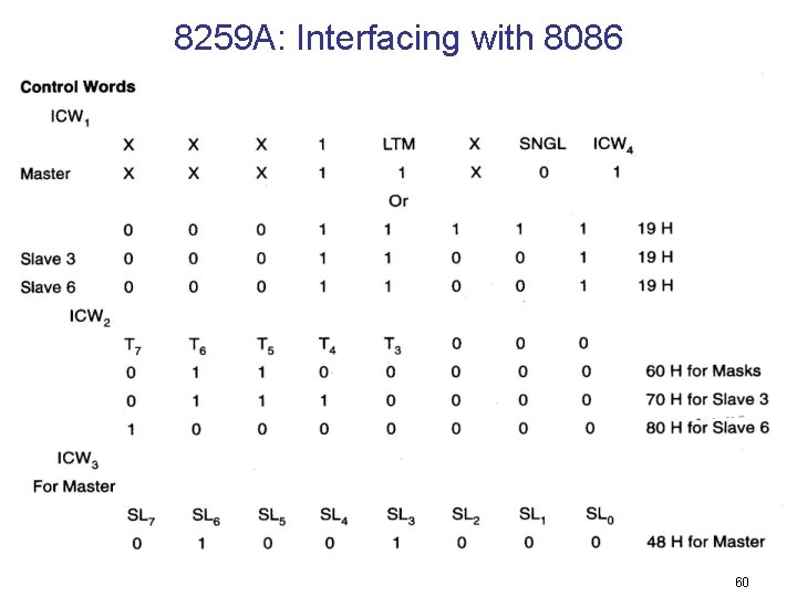
8259 A: Interfacing with 8086 60
8259 A: Interfacing with 8086 61
8259 A: Interfacing with 8086 62
8279: Keyboard/Display Controller • Intel’s 8279 is a general purpose keyboard display controller that simultaneously drives the display of a system and interfaces a key board with the CPU, leaving it free for its routine task. • The key board display interface scans the key board to identify if any 7 key has been pressed and sends the code of the pressed key to the CPU. • It also transmits the data received from the CPU, to the display device. • Both of these functions are performed by the controller in repetitive fashion without involving the CPU. • The key board display controller chip 8279 provides – (a) set of four scan lines and eight return lines for interfacing key boards – (b) a set of eight output lines for interfacing display. 63
8279: Keyboard/Display Controller • I/O control and Data buffers – The I/O control section controls the flow of data to / from the 8279. – The data buffers interface the external bus of the system with internal bus of 8279. – The I/O section is enabled only if D bar is low. – The pins A 0, RD bar and WR bar select the command, status or data read/ write operations carried out by the CPU with 8279. • Control and Timing Register and Timing Control – These registers store the key board and display modes and other operating conditions programmed by CPU. – The registers are written with A 0 = 1 and WR bar =0. 64
8279: Keyboard/Display Controller • Scan Counter – The scan counter has two modes to scan the key matrix and refresh the display. – In the second encoded mode, the counter provides a binary count that is to be externally decoded to provide the scan lines for key board and display (four externally decoded scan lines may drive up to 16 displays). – n the decoded scan mode, the counter internally decodes the least significant 2 bits and provides a decoded 1 out of 4 scan on SL 0 – SL 3 (four internally decoded scan lines may drive up to 4 displays). – The key board and display both are in the same mode at a time. • Return Buffers and Keyboard Debounce and Control: – This section scans for a key closure row-wise. I – f it is detected, the keyboard debounce unit debounces the key entry (i. e. wait for 10 ms). – After the debounce period, if the key continues to be detected. – The code of the key is directly transferred to the sensor RAM along with SHIFT and CONTROL key status. 65
8279: Keyboard/Display Controller • FIFO/Sensor RAM and Status Logic : – In keyboard or strobed input mode, this block acts as 8 byte first in first out (FIFO) RAM. – Each key code of the pressed key is entered in the order of the entry, and in the mean time, read by the CPU, till the RAM becomes empty. – In scanned sensor matrix mode, this unit acts as sensor RAM. • Display Address Registers and Display RAM : – The display address registers hold the address of the word currently being written or read by the CPU to or from the display RAM. 66
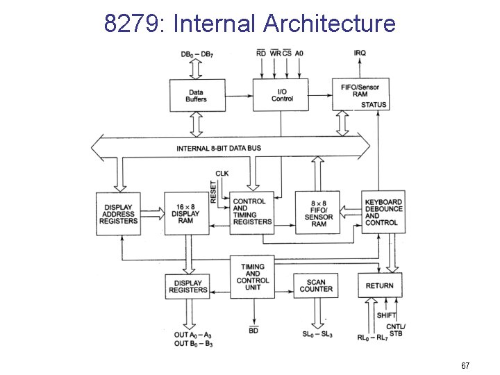
8279: Internal Architecture 67
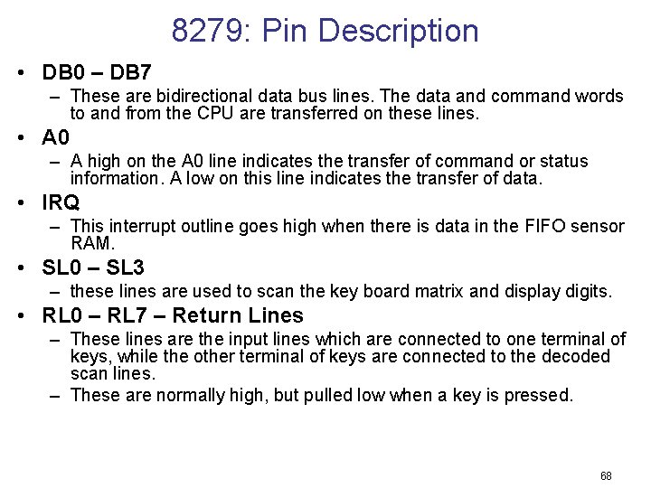
8279: Pin Description • DB 0 – DB 7 – These are bidirectional data bus lines. The data and command words to and from the CPU are transferred on these lines. • A 0 – A high on the A 0 line indicates the transfer of command or status information. A low on this line indicates the transfer of data. • IRQ – This interrupt outline goes high when there is data in the FIFO sensor RAM. • SL 0 – SL 3 – these lines are used to scan the key board matrix and display digits. • RL 0 – RL 7 – Return Lines – These lines are the input lines which are connected to one terminal of keys, while the other terminal of keys are connected to the decoded scan lines. – These are normally high, but pulled low when a key is pressed. 68
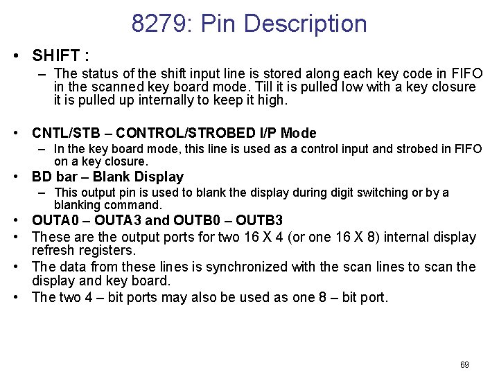
8279: Pin Description • SHIFT : – The status of the shift input line is stored along each key code in FIFO in the scanned key board mode. Till it is pulled low with a key closure it is pulled up internally to keep it high. • CNTL/STB – CONTROL/STROBED I/P Mode – In the key board mode, this line is used as a control input and strobed in FIFO on a key closure. • BD bar – Blank Display – This output pin is used to blank the display during digit switching or by a blanking command. • OUTA 0 – OUTA 3 and OUTB 0 – OUTB 3 • These are the output ports for two 16 X 4 (or one 16 X 8) internal display refresh registers. • The data from these lines is synchronized with the scan lines to scan the display and key board. • The two 4 – bit ports may also be used as one 8 – bit port. 69
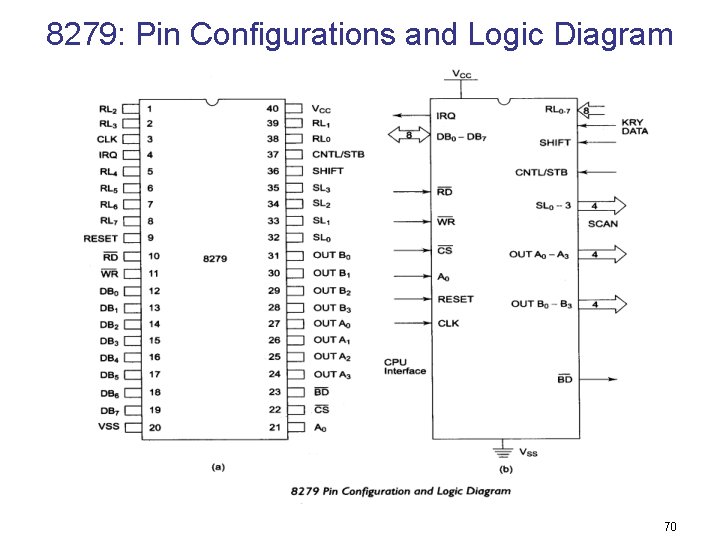
8279: Pin Configurations and Logic Diagram 70
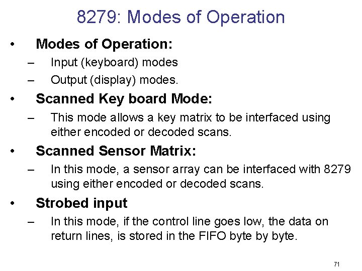
8279: Modes of Operation • Modes of Operation: – – • Input (keyboard) modes Output (display) modes. Scanned Key board Mode: – • This mode allows a key matrix to be interfaced using either encoded or decoded scans. Scanned Sensor Matrix: – • In this mode, a sensor array can be interfaced with 8279 using either encoded or decoded scans. Strobed input – In this mode, if the control line goes low, the data on return lines, is stored in the FIFO byte by byte. 71
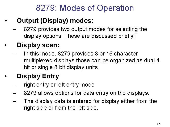
8279: Modes of Operation • Output (Display) modes: – • 8279 provides two output modes for selecting the display options. These are discussed briefly: Display scan: – • In this mode, 8279 provides 8 or 16 character multiplexed displays those can be organized as dual 4 bit or single 8 bit display units. Display Entry – – – right entry or left entry mode 8279 allows options for data entry on the displays. The display data is entered for display either from the right side or from the left side. 72
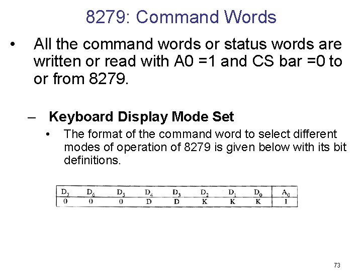
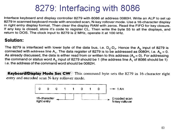
8279: Command Words • All the command words or status words are written or read with A 0 =1 and CS bar =0 to or from 8279. – Keyboard Display Mode Set • The format of the command word to select different modes of operation of 8279 is given below with its bit definitions. 73
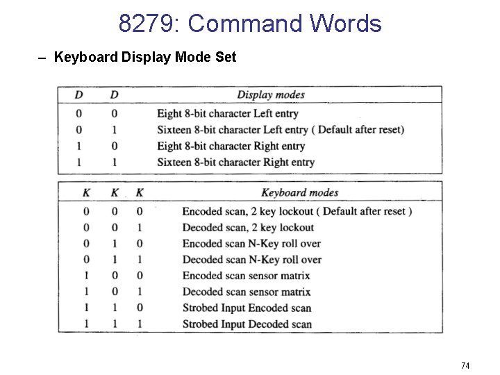
8279: Command Words – Keyboard Display Mode Set 74
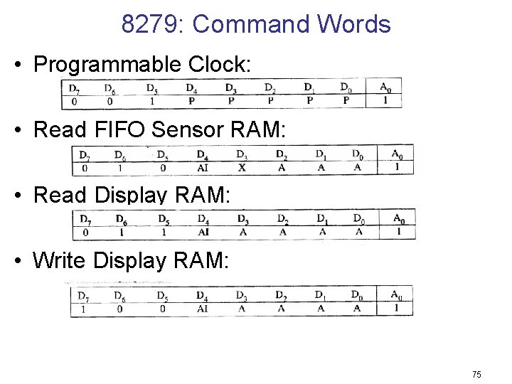
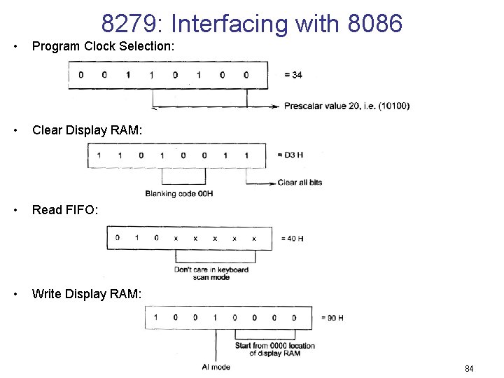
8279: Command Words • Programmable Clock: • Read FIFO Sensor RAM: • Read Display RAM: • Write Display RAM: 75
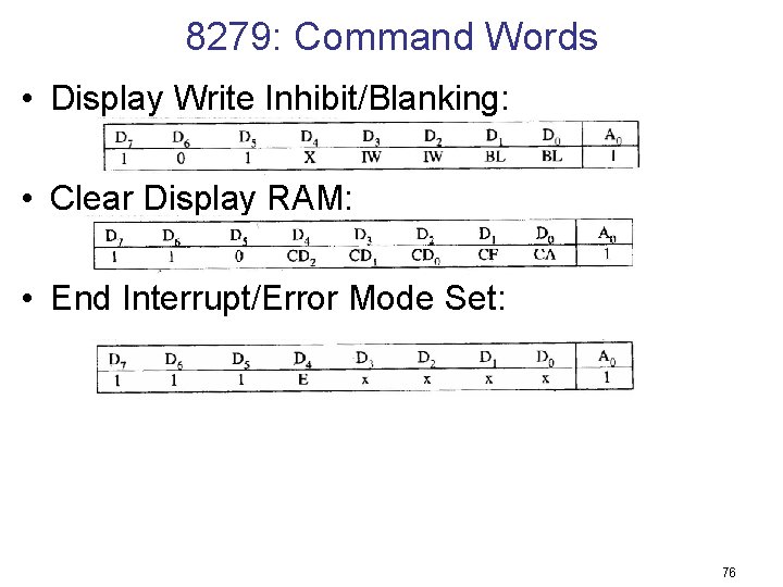
8279: Command Words • Display Write Inhibit/Blanking: • Clear Display RAM: • End Interrupt/Error Mode Set: 76
8279: Command Words – Read Display RAM This command enables a programmer to read the display RAM data. – Display Write inhibit/Blanking The IW (Inhibit Write flag) bits are used to mask the individual nibble as shown in the above command. – Clear Display RAM The CD 2, CD 1, CD 0 is a selectable blanking code to clear all the rows of the display RAM as given below. – CD 2 must be 1 for enabling the clear display command. – For the sensor matrix mode, this command lowers the IRQ line and enables further writing into the RAM. 77
8279: Command Words – Programmable Clock The clock for operation of 8279 is obtained by dividing the external clock input signal by a programmable constant called prescaler. – PPPPP is a 5 bit binary constant. The input frequency is divided by a decimal constant ranging from 2 to 31, decided by the bits of an internal prescaler, PPPPP. 78
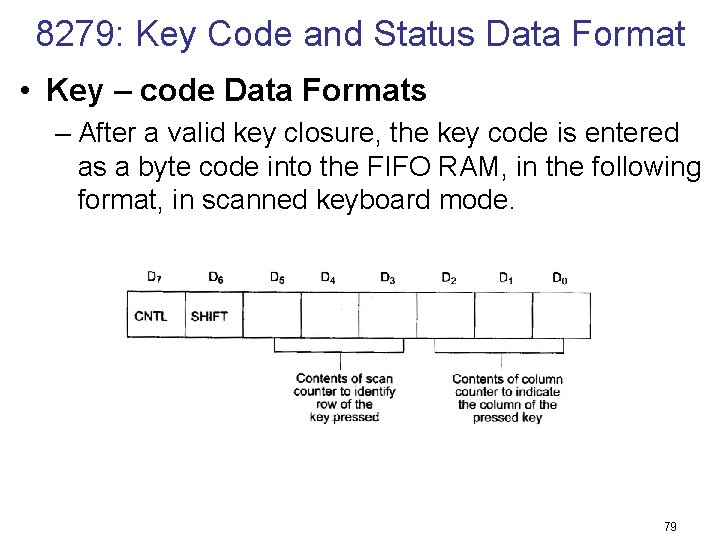
8279: Key Code and Status Data Format • Key – code Data Formats – After a valid key closure, the key code is entered as a byte code into the FIFO RAM, in the following format, in scanned keyboard mode. 79
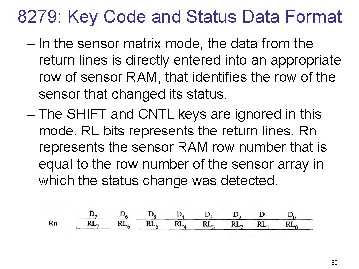
8279: Key Code and Status Data Format – In the sensor matrix mode, the data from the return lines is directly entered into an appropriate row of sensor RAM, that identifies the row of the sensor that changed its status. – The SHIFT and CNTL keys are ignored in this mode. RL bits represents the return lines. Rn represents the sensor RAM row number that is equal to the row number of the sensor array in which the status change was detected. 80
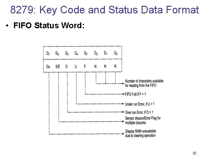
8279: Key Code and Status Data Format • FIFO Status Word: – The FIFO status word is used in keyboard and strobed input mode to indicate the error. – Overrun error occurs, when an already full FIFO is attempted an entry. – Under run error occurs when an empty FIFO read is attempted. – FIFO status word also has a bit to show the unavailability of FIFO RAM because of the ongoing clearing operation. – The status word contains FIFO status, error and display unavailable signals. – This is read, when A 0=1, RD Bar=0 and CS Bar =0. Data is read when A 0, CS Bar, RD bar are low. 81
8279: Key Code and Status Data Format • FIFO Status Word: 82
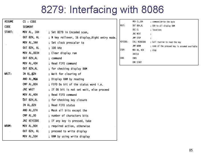
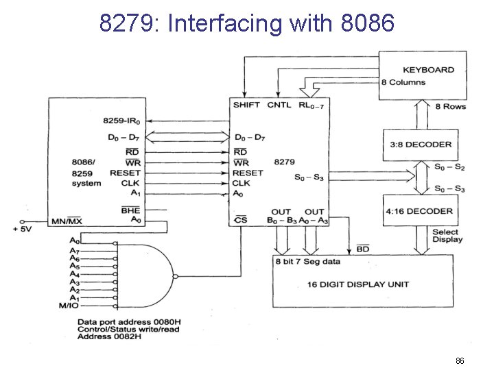
8279: Interfacing with 8086 Solution: 83
8279: Interfacing with 8086 • Program Clock Selection: • Clear Display RAM: • Read FIFO: • Write Display RAM: 84
8279: Interfacing with 8086 85
8279: Interfacing with 8086 86
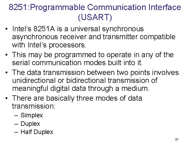
8251: Programmable Communication Interface (USART) • Intel’s 8251 A is a universal synchronous asynchronous receiver and transmitter compatible with Intel’s processors. • This may be programmed to operate in any of the serial communication modes built into it. • The data transmission between two points involves unidirectional or bidirectional transmission of meaningful digital data through a medium. • There are basically three modes of data transmission: – Simplex – Duplex – Half Duplex 87
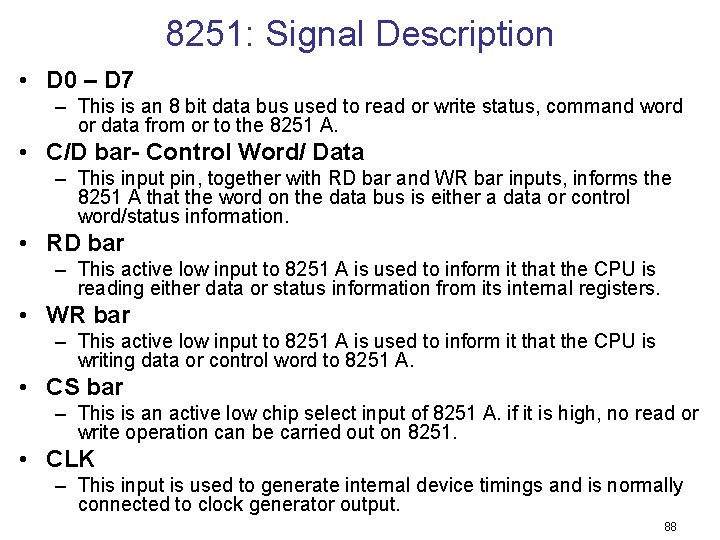
8251: Signal Description • D 0 – D 7 – This is an 8 bit data bus used to read or write status, command word or data from or to the 8251 A. • C/D bar- Control Word/ Data – This input pin, together with RD bar and WR bar inputs, informs the 8251 A that the word on the data bus is either a data or control word/status information. • RD bar – This active low input to 8251 A is used to inform it that the CPU is reading either data or status information from its internal registers. • WR bar – This active low input to 8251 A is used to inform it that the CPU is writing data or control word to 8251 A. • CS bar – This is an active low chip select input of 8251 A. if it is high, no read or write operation can be carried out on 8251. • CLK – This input is used to generate internal device timings and is normally connected to clock generator output. 88
8251: Signal Description • RESET – A high on this input forces the 8251 A into an idle state. • TXC bar Transmitter Clock Input – This transmitter clock input controls the rate at which the character is to be transmitted. • TXD Transmitted Data Output – This output pin carries serial stream of the transmitted data bits along with other information like start bit, stop bits and parity bit, etc. • RXC bar receiver Clock Input – This receiver clock input pin controls the rate at which the character is to be received. • RXD- Receive Data Input – This input pin of 8251 A receives a composite stream of the data to be received by 8251 A. 89
8251: Signal Description • RXRDY – Receiver Ready Output – This output indicates that the 8251 A contains a character to be read by the CPU. The RXRDY signal may be used either to interrupt the CPU or may be polled by the CPU. • TXRDY – Transmitter Ready – This output indicates to the CPU that the internal circuit of the transmitter is ready to accept a new character for transmission from the CPU. • DSR bar – Data Set Ready – The input may be use d as a general purpose one bit inverting input port. Its status can be checked by the CPU using a status operation. • DTR Bar – Data Terminal Ready – This output may be used as a general purpose one bit inverting output port. • RTS Bar – Request to Send Data – This output may be used as a general purpose one bit inverting output port that can be programmed low to indicate the modem that the receiver is ready to receive a data byte from the modem. – This signal is used to communicate with a modem. 90
8251: Signal Description • CTS Bar – Clear to Send – If the clear to send the input line is low, the 8251 A is enabled to transmit the serial data, provided the enable bit in the command byte is set to ‘ 1’. • TXE – Transmitter Empty – If the 8251 A, while transmitting, has no characters to transmit, the TXE output goes high and it automatically goes low when a character is received from the CPU, for further transmission. • SYNDET/BD – Synch Detect/Break Detect – This pin is used in the synchronous mode for detecting SYNC characters (SYNDET) and may be used as either input or output. 91
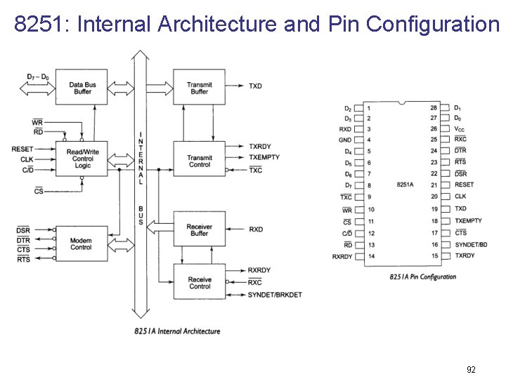
8251: Internal Architecture and Pin Configuration 92
8251: Operating Modes • The 8251 can be programmed to operate in its various modes using its mode control words. • The control words of 8251 A are divided into two functional types: – Mode Instruction control word – Command instruction control word. • Asynchronous Mode – Mode Instruction control word • This defines the general operational characteristics of 8251 A after internal (reset command) or external (reset input pin) reset, this must be written to configure the 8251 A as per the required operation. • To change the mode of operation from synchronous to asynchronous or vice - versa, the 8251 A has to be reset using master chip reset. 93
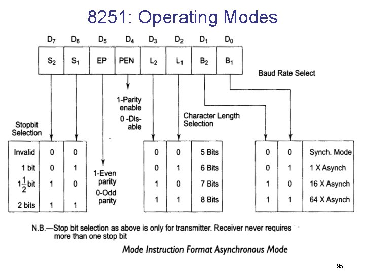
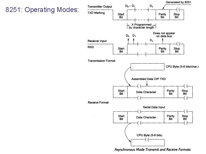
8251: Operating Modes • Asynchronous Mode (Transmission) – When a data character is sent to 8251 A by the CPU, it adds start bits prior to the serial data bits, followed by optional parity bit and stop bits using the asynchronous mode instruction control format. – This sequence is then transmitted using TXD output pin on the falling edge of TXC bar. • A synchronous Mode (Receive) – A falling edge on RXD input line marks a start bit. – At baud rates of 16 x and 64 x, this start bit is again checked at the center of start bit pulse and if detected low, it is a valid start bit which starts counting. 94
8251: Operating Modes 95
8251: Operating Modes: 96
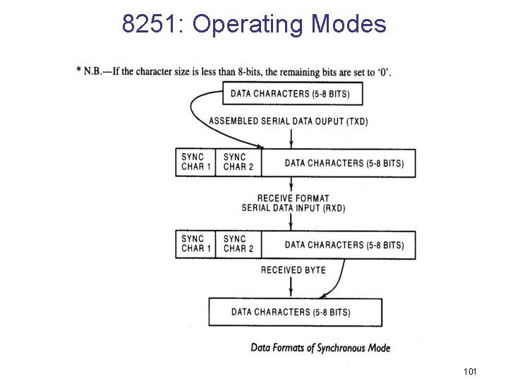
8251: Operating Modes • Synchronous Mode – Synchronous Mode (Transmission) • The TXD output is high until the CPU sends a character to 8251 A which is usually is a SYNC character. • When CTS bar line goes low, the first character is serially transmitted out. • All the characters are shifted out on the falling edges of TXC bar. • Data is shifted out at the same rate as TXc bar, over TXD output line. • If the CPU buffer becomes empty, the SYNC character or characters are inserted in the data stream over TXD output. – Synchronous Mode (Receiver) • In this mode, the character synchronization can be achieved internally or externally. • If this mode is programmed, then ‘ENTER HUNT’ command should be included in the first command instruction word written into the 8251 A. • The data on RXD pin is sampled on rising edge of the RXC bar. • The content of the receiver buffer is compared with the first SYNC character at every edge until it matches. 97
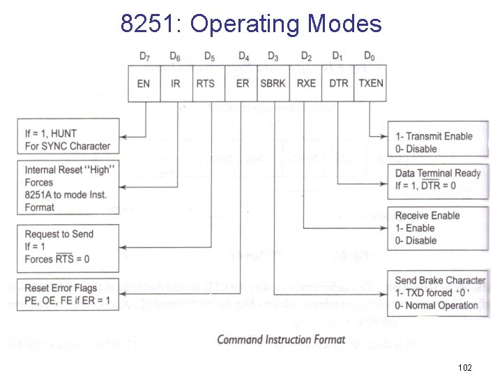
– Command Instruction Definition • The command instruction controls the actual operations of the selected format like enable transmit/receive, error reset and modem control. • Once the mode instruction has been written 8251 A and the SYNC characters are inserted internally by 8251 A, all further control words written with C/D =1 will load a command instruction. • A reset operation returns 8251 A back to mode instruction format. 98
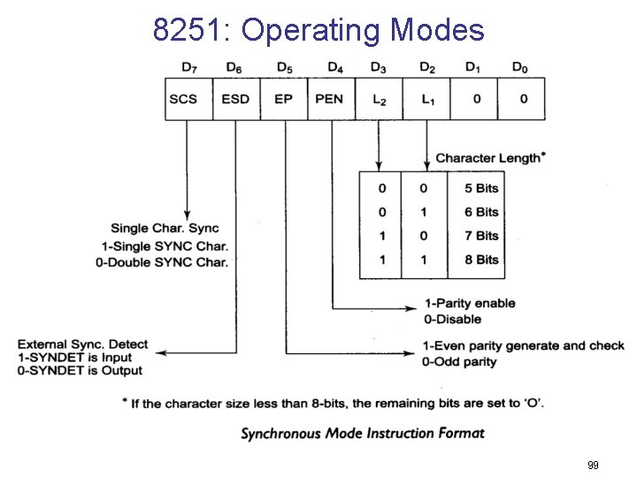
8251: Operating Modes 99
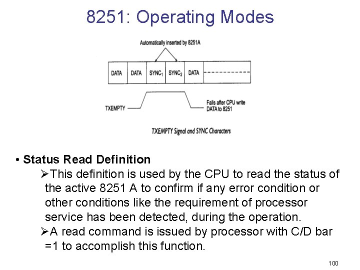
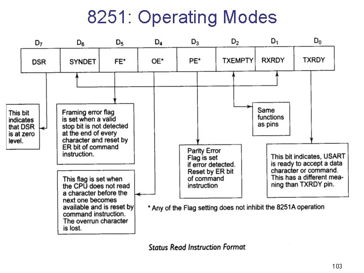
8251: Operating Modes • Status Read Definition ØThis definition is used by the CPU to read the status of the active 8251 A to confirm if any error condition or other conditions like the requirement of processor service has been detected, during the operation. ØA read command is issued by processor with C/D bar =1 to accomplish this function. 100
8251: Operating Modes 101
8251: Operating Modes 102
8251: Operating Modes 103
8251: Interfacing with 8086 104
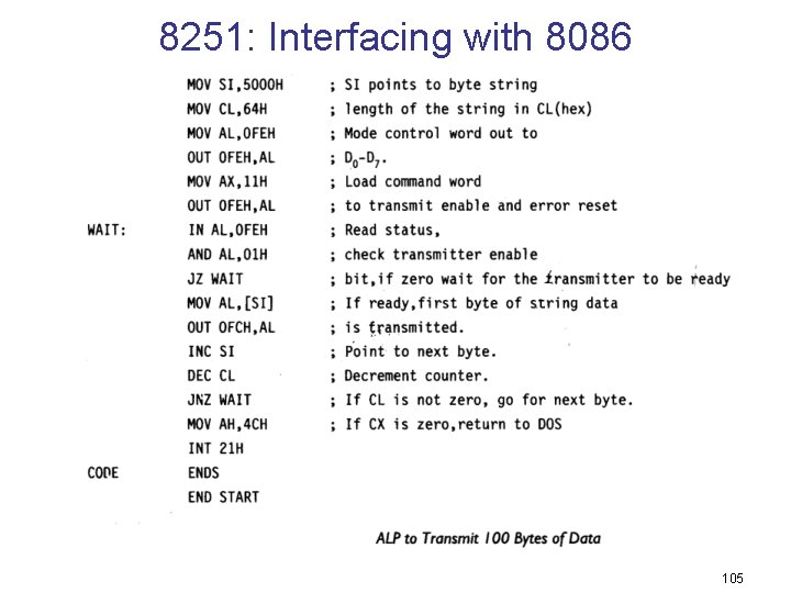
8251: Interfacing with 8086 105
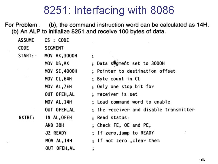
8251: Interfacing with 8086 106
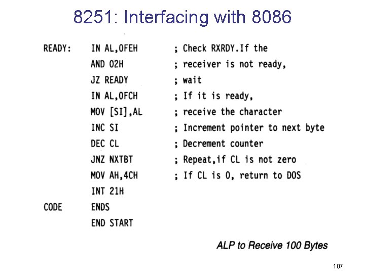
8251: Interfacing with 8086 107
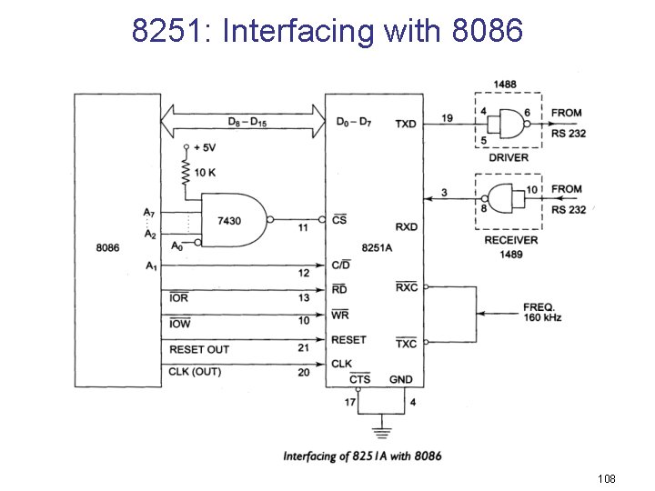
8251: Interfacing with 8086 108
- Slides: 108