Sony Play Station 3 Sony also laid out
- Slides: 6

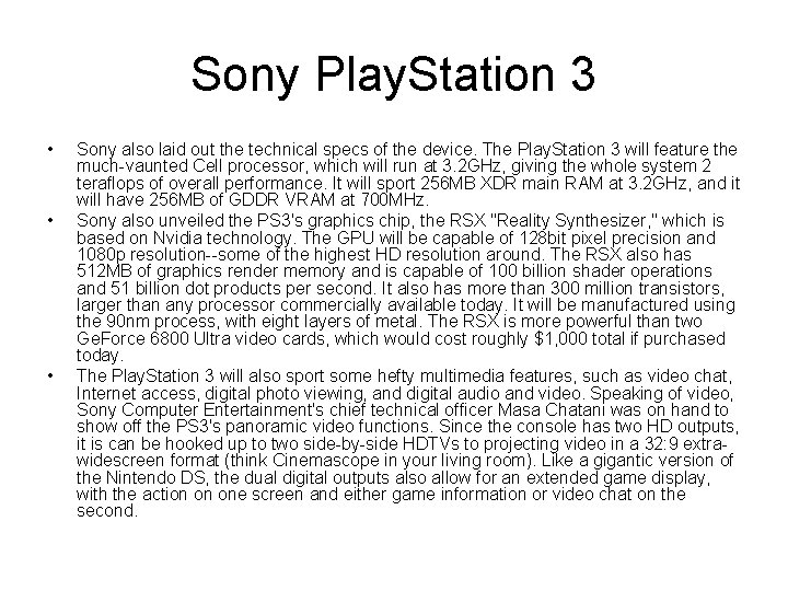
Sony Play. Station 3 • • • Sony also laid out the technical specs of the device. The Play. Station 3 will feature the much-vaunted Cell processor, which will run at 3. 2 GHz, giving the whole system 2 teraflops of overall performance. It will sport 256 MB XDR main RAM at 3. 2 GHz, and it will have 256 MB of GDDR VRAM at 700 MHz. Sony also unveiled the PS 3's graphics chip, the RSX "Reality Synthesizer, " which is based on Nvidia technology. The GPU will be capable of 128 bit pixel precision and 1080 p resolution--some of the highest HD resolution around. The RSX also has 512 MB of graphics render memory and is capable of 100 billion shader operations and 51 billion dot products per second. It also has more than 300 million transistors, larger than any processor commercially available today. It will be manufactured using the 90 nm process, with eight layers of metal. The RSX is more powerful than two Ge. Force 6800 Ultra video cards, which would cost roughly $1, 000 total if purchased today. The Play. Station 3 will also sport some hefty multimedia features, such as video chat, Internet access, digital photo viewing, and digital audio and video. Speaking of video, Sony Computer Entertainment's chief technical officer Masa Chatani was on hand to show off the PS 3's panoramic video functions. Since the console has two HD outputs, it is can be hooked up to two side-by-side HDTVs to projecting video in a 32: 9 extrawidescreen format (think Cinemascope in your living room). Like a gigantic version of the Nintendo DS, the dual digital outputs also allow for an extended game display, with the action on one screen and either game information or video chat on the second.

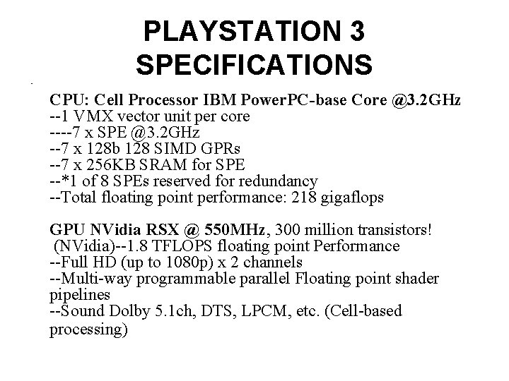
• PLAYSTATION 3 SPECIFICATIONS CPU: Cell Processor IBM Power. PC-base Core @3. 2 GHz --1 VMX vector unit per core ----7 x SPE @3. 2 GHz --7 x 128 b 128 SIMD GPRs --7 x 256 KB SRAM for SPE --*1 of 8 SPEs reserved for redundancy --Total floating point performance: 218 gigaflops GPU NVidia RSX @ 550 MHz, 300 million transistors! (NVidia)--1. 8 TFLOPS floating point Performance --Full HD (up to 1080 p) x 2 channels --Multi-way programmable parallel Floating point shader pipelines --Sound Dolby 5. 1 ch, DTS, LPCM, etc. (Cell-based processing)

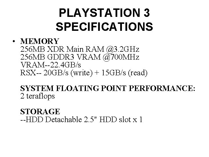
PLAYSTATION 3 SPECIFICATIONS • MEMORY 256 MB XDR Main RAM @3. 2 GHz 256 MB GDDR 3 VRAM @700 MHz VRAM--22. 4 GB/s RSX-- 20 GB/s (write) + 15 GB/s (read) SYSTEM FLOATING POINT PERFORMANCE: 2 teraflops STORAGE --HDD Detachable 2. 5" HDD slot x 1

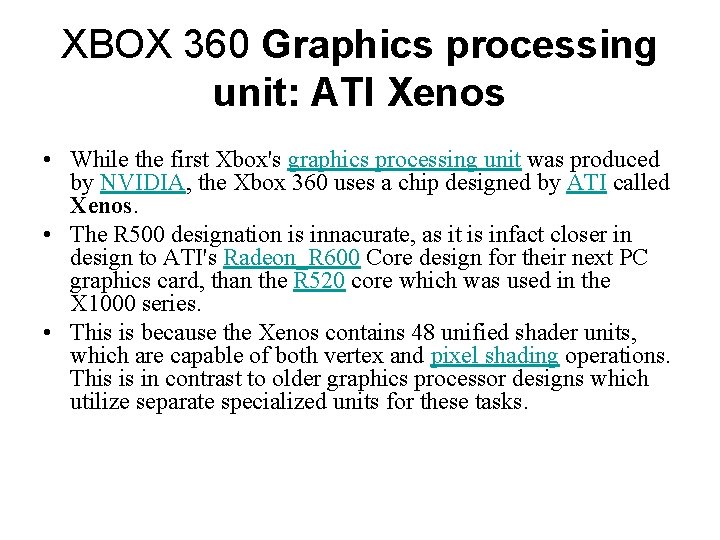
XBOX 360 Graphics processing unit: ATI Xenos • While the first Xbox's graphics processing unit was produced by NVIDIA, the Xbox 360 uses a chip designed by ATI called Xenos. • The R 500 designation is innacurate, as it is infact closer in design to ATI's Radeon_R 600 Core design for their next PC graphics card, than the R 520 core which was used in the X 1000 series. • This is because the Xenos contains 48 unified shader units, which are capable of both vertex and pixel shading operations. This is in contrast to older graphics processor designs which utilize separate specialized units for these tasks.

XBOX 360 Graphics processing unit: ATI Xenos • The GPU package contains two separate silicon dies, each on a 90 nm chip with a clock speed of 500 MHz; the GPU proper, manufactured by TSMC and a 10 Mi. B e. DRAM daughter-die, manufactured by NEC. Thanks to the daughter die, the Xenos can do 4 x FSAA, z-buffering, and alpha blending with no appreciable performance penalty on the GPU. [50]

XBOX 360 CPU • The CPU, named Xenon at Microsoft and "Waternoose" at IBM, is a custom triple-core Power. PC-based design by IBM. The CPU emphasizes high floating point performance through multiple FPU and SIMD vector processing units in each core. It has a theoretical peak performance of 115. 2 gigaflops and is capable of 9. 6 billion dot products per second. Each core of the CPU is simultaneous multithreading capable and clocked at 3. 2 gigahertz. The original chip uses a 90 nanometer process, although a 65 nanometer process SOI revision was originally planned for early 2007, [46] but it has been delayed until mid-2007. [47] A 21. 6 GB/s front side bus, aggregated 10. 8 GB/s upstream and downstream, connects Xenon with the graphics processor/northbridge. Xenon is equipped with a 1 Mi. B Level 2 cache on-die running at half CPU clock speed. This cache is shared amongst the three CPU cores. [48]