Solving the Information Technology Energy Challenge Beyond Moores

Solving the Information Technology Energy Challenge Beyond Moore’s Law Search for a New Moore’s Law

Old Moore’s Law: 2 x Transistor Density every 12 -24 Months at same power & cost!

The problem: IT projected to challenge future electricity supply Even worse if Moore’s Law ends!!! 10000 TWHr 8000 6000 4000 Projection based on consumer electronics + data centers MORE MOORE’S BIG IDEA 2000 0 2005 2010 2015 Year 2020 2025 www. alliancetrustinvestments. com/sri-hub/posts/Energy-efficient-data-centres www. iea. org/publications/freepublications/publication/gigawatts 2009. pdf 2030

50 Atomic scale limit case for 2 D Lithography Scaling 2027? 5 nm
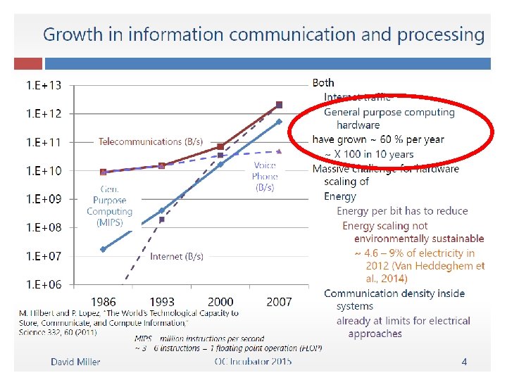
 Transistors Performance Thread Performance Clock Frequency Power (watts)")
Technology Scaling Trends (more flattening ahead) Transistors Performance Thread Performance Clock Frequency Power (watts) # Cores Year Figure courtesy of Kunle Olukotun, Lance Hammond, Herb Sutter, and Burton Smith

Post-Lithographic Scaling Options 20+ years scaling w/20 year lead There are other ways to continue Moore’s Scaling! New Scaling Law for 10 years scaling After 2025 ?

Fundamental Materials Science Drivers Design of hierarchical ground states for multistate memories and logic Manipulate information at the limits of Energy : 1 Atto. Joule switch Energy-efficient synthesis of new forms of matter with tailored properties Control of correlations and emergent behavior @m. V scale Control of electron wavefunctions
 Computing Science (ASCR) Manufacturing Science (AMO) • Leverage unique")
The Opportunity Fundamental Science (BES) Computing Science (ASCR) Manufacturing Science (AMO) • Leverage unique capabilities in material science • Advanced computing • Move revolutionary low energy devices and architectures from Lab to Fab • Scientific user facilities • Multiscale computing benchmarking and modeling • Computational approaches to materials design • Next-generation heterogeneous architectures • Accelerate development and manufacturing base for electronic devices • Grand challenges driven research • New programming models and application software • Create public-private partnerships with electronics industry

Beyond Moore Codesign Framework 10, 000 x improvement: 20 f. J per instruction equivalent Application Performance Modeling Sy ste ms Computer System Architecture Modeling • Next generation of Structural Simulation Toolkit • Heterogeneous systems HPC models Component Level Models • Gem 5, Mc. PAT, Hi. HAT, CACTI, NVSIM Component Fabrication • Processors, ASICs • Photonics • Memory Test Circuit Fab and Measurement • Subcircuit measurement Compact Device Models • Single device electrical models • Variability and corner models Device Measurements • Single device electrical behavior • Parametric variability vic es Circuit/IP Block Design and Modeling • SPICE/Xyce model De TEM/EELS Device Physics Modeling • Device physics modeling (TCAD) • Electron transport, ion transport • Magnetic properties Device Structure Integration and Demonstration • Novel device structure demonstration Process Module Demonstrations • EUV and novel lithography • Diffusion, etch, implant simulation ter Ma Atomistic and Ab-Initio Modeling • DFT – VASP • MD – LAAMPS ial s Process Module Modeling • Diffusion, etch, implant simulation • EUV and novel lithography models Fundamental Materials Science • X-ray: XRD, XPS, HAXPES • Microscopy: TEM, SEM, EELS • Scanning probe technique Experimental

Syn Nan thesi osc s ale Cen ters nof (N a (Lig Chara ht S cter pho ourc izati o e ton s, elec n eut ron trons, s, … ) ab, s, e y d er n co ) v o c o Dis ulati ting, … im mpu s l ria ip co e t (ma dersh lea , …) Advanced Materials

Syn Nan thesi osc s ale Cen ters s, e y d er n co ) v o c o Dis ulati ting, … im mpu s l ria ip co e t (ma dersh lea , …) Advanced Materials nof (N a (Lig Chara ht S cter pho ourc izati o e ton s, elec n eut ron trons, s, … ) ab, Goal: Goal Accelerate discovery of materials with improved properties for energy efficient electronics by factor of 1000 x.

Advanced Devices and Manufacturing (3 D Tom Tes Spe ograp t ctro h sco y, Ion py, etc beam …) (EU V d Mo Fab /EU ricat ME REKA, e SAF e ab, -Beam …) e) t l l u a de tion omp o M uta ve C p ssi m o C , Ma w (Ne lation u m i el/S

Advanced Devices and Manufacturing (CX Fab RO, rica t E ME UV/E e URE SAF ab, K …) A, e) t l l u a de tion omp o M uta ve C p ssi m o C , Ma w (Ne lation u m i el/S d devices with manufacturing path to Goal: Goal Discover new Mo enable next 30 years of Moore’s scaling. (3 D Tom Tes o Spe grap t ctro h sco y, Ion py, etc. beam. . )

Architecture & Algorithms Ben nch chmar ma kin r k, a g app n lica tion alyze, s) (Be Syn (Op thesis /Pr en. S OC, oto ME type SAF ab) rs. . ) o t la ign. u im des S l a s, co r u ct del e t i h l, mo c r A se i h C , T (SS

Architecture & Algorithms Syn (Op thesis /Pr en. S OC, oto ME type SAF ab) rs. . ) o t la ign. u im des S l a s, co r u ct del e t i h l, mo c r A se i h C , T Accelerate (SS discovery and validation Goal: of Goal architecture improvements using new device technologies. (scale-bridging) Ben nch chmar ma kin r k, a g app n lica tion alyze, s) (Be

National Lab Partnerships Opportunities Today’s CMOS Voltage limit at M er t t e B Com More Effi put cien ing Arc t hite ctu r Bet ter Dev ices Interesting materials!!! s l a i er e

Building a Public-Private Partnership

10000 SUMMARY TWHr 8000 6000 100’s fewer power plants 4000 2000 2005 2010 2015 Year 2020 2025 2030 • Looming end of Moore’s Law creating rapidly growing energy gap • Coordinated public-private partnership will drive breakthroughs by leveraging multiple DOE Office leadership and Lab capabilities Success IS: continued growth and affordability of our information economy, with US Economic impact in Trillions$

BACKUP

Atomistic holistic device simulation v Atomistic DFT simulations, beyond TCAD v Useful for new materials and designs v Whole device with >100, 000 atoms v Petascale to exascale HPC v Codes exist, need to be integrated LS 3 DF + FSM for > 10, 000 atoms DFT I/V curve (LCBB for million atoms) HP 4 mfg with Global Foundry Mo. S 2 for TFET (PEtot_trans for transport calc. ) Integrate the existing codes to form a package for holistic ab initio device simulation

Longer-Term Impacts • HPC data mining and “Inverse Design” are starting to become “standard business practice”. • Exascale success will enable bigger applications to drive demand for large scale compute cycles and energy. • The countries that can circumvent the energy challenges to enable the HPC applications that will discover future disruptions in Manufacturing, Climate, Medicine, and Energy will dominate the future world economy. “Beyond Moore’s Law” technologies will also address the energy challenges of the ~21 M Io. T units to be deployed by 2020 (vampire loads). “Traditionally disruptions are caused by emergence of a different kind of material, different kind of process, or a different way of doing something. Those cited here are expected to completely upstage the worldwide economy by 2025, ” Dr. Sadasivan Shankar, prominent Intel materials scientist, “In Silico Inverse Design” http: //www. hpcwire. com/2015/06/15/fixating-on-exascale-performance-only-is-a-bad-idea/

The semiconductor industry is crucial to the U. S. economy. Semiconductor sales constitute a $336 B/yr. economic engine driving the $2. 3 T/yr. global electronics industry. Semiconductor products are currently the second largest class of U. S. exports; U. S. companies account for more t

IT already accounts for 5% of global electricity usage and growing fast • In 2012, ICT usage consumed 4. 7 percent of electricity worldwide, amounting to approximately 920 TWh (1 TWh is a terawatthour or 1012 watt-hours) – Source: The EINS Consortium. Overview of ICT energy consumption (D 8. 1). Report FP 7 - 2888021. European Network of Excellence in Internet Science. February 2013. – Van Heddeghem, W. , Lambert, S. , Lanoo, B. , Colle, D. , Pickavet, M. , and Demeester, P. Trends in worldwide ICT electricity consumption from 2007 to 2012. Computer Communications 50 (2014), 64 -76.

Gadgets and Gigawatts report https: //www. iea. org/publications/freepublications/publication/gigawatts 2009. pdf

Datacenter electricity use also exploding Energy efficient data centers, Harriet Parker, SRI Analyst, 19 February 2013 www. alliancetrustinvestments. com/sri-hub/posts/Energy-efficient-data-centres
 – Materials and devices for")
Result of Big Idea • Fundamentals & Devices: (BES/AMO) – Materials and devices for 20 f. J per effective instruction (vs. 200 p. J/instruction today) • Computing: (ASC/ASCR) – Accelerate the development and introduction of next generation computing via device-to-arch framework • Manufacturing: (EERE/AMO, NNSA) – enhance US position in semiconductor manufacturing • Overall Energy Savings: (USA) – “Cut 2030 ICT energy usage by 50%” – Enable continued growth of mobile connectivity and application of HPC to our info economy (keep up with the rest of the world)

Fig. 5. Evolution of worldwide electricity use of networks, PCs and data centers (solid lines, left axis) and total worldwide electricity use (dotted line, right axis). Over the last five years, the electricity consumption in all three ICT categories increased at a rate higher than the total worldwide electricity consumption. In 2012 each category accounts for roughly 1. 5% of the worldwide electricity consumption. Note that, since some of the data points between 2007 and 2012 are based on interpolations, small variations might not show up in the intermediate years

Coming explosion of always “on” Io. T devices Table 1: Internet of Things Units Installed Base by Category (Millions of Units) Source: Gartner (November 2015) Category Consumer Business: Cross. Industry Business: Vertical-Specific Grand Total 2014 2, 277 632 2015 3, 023 815 2016 4, 024 1, 092 2020 13, 509 4, 408 898 1, 065 1, 276 2, 880 3, 807 4, 902 6, 392 20, 797

Beyond Moore’s Law Photonics - > $1/Gb/s - 25 p. J/bit Both Too High Today’s Petascale computing utilize optical transceivers for the ‘network’ interconnect 10 -20 years: Need “Beyond Moore” Photonics • Scale Energy and Cost by 104 1 f. J/bit optics complete (>25, 000 X equivalent) 0. 01¢ Gb/s ($10¢/Tb/s) (>10, 000 X equivalent) • New Materials, Devices, Components • Interface to LV-CMOS and beyond-Moore’s transistor devices 5 -10 years: Commodity Integrated Photonics • • • Hetero-Integrated CMOS photonics manufacturing Drastically lower the cost of packaging Higher data rate per optical IO, further reduction 25 p. J/bit < 1 p. J/bit optics total (> 25 X) $1/Gb/s 10¢ Gb/s ($100/Tb/s) (10 X) – • • TFETs, Quantum, Neuromorphic, etc. Optical switching, routing, computing Optical modeling infrastructure – Optical materials, devices sub-systems application impact

The path: near and long term Need more efficient materials/devices for next 10 -20+ years Revolutionary Heterogeneous HPC architectures & software Photonic ICs More efficient architecture in first 10 years

The path: near and long term Attojoule Switch Materials with hierarchical Atomic scaleground states Control of correlations Computing with Electron wavefunctions Photonic ICs

New Devices and materials y Atomic-scale Control of Attojoule Correlations Hierarchical Ground Switch States Compute with Electronic Spintronics Wave-functions Carbon Nanotubes Graphene PET Dark Silicon TFETs Neuromorphic of s el n d o M tatio w u Ne mp Dataflow Co Quantum z Analog Adabiatic Reversible Approximat e Computing Superconducting 3 D Stacking Adv. Packages CMOS General Purpose Syste m on Chip NTV Reconfigurabl e Computing Dark Silicon New Architectures and Packaging x

Attojoule Switch New Devices and materials y Spintronics Carbon Nanotubes Graphene PET TFETs CMOS 3 D Stacking General Purpose System on Chip NTV Reconfigurable Computing Dark Silicon New Architectures and Packaging x

Complex Landscape SRC IARPA NSF DOE/National Labs Industry • • Support Collaborate Partnerships Early Adoption Academia DARPA

Multi-Lab Engagement Ramamoorthy Ramesh Patrick Naulleau John Shalf Horst Simon Gary Grider John Sarrao Toni Taylor Trish Damkroger Jeff Nichols Lou Terminello Nathan Baker Malin Young Supratik Guha Rick Stevens (F. B. ) Rick Mc. Cormick Bruce Hendrickson Dave Sandison Rob Leland
 Discovery ✔ ✔ Synthesis (Nanoscale Centers, Nanofab, etc…) ✔ ✔")
Area Activity Materials (BES) Discovery ✔ ✔ Synthesis (Nanoscale Centers, Nanofab, etc…) ✔ ✔ ✔ ✔ Characterization (Electron, photon, neutron) ✔ ✔ ✔ Model (HPC 4 Mfg, HPC) ✔ ✔ ✔ Fabricate (MESAFab, CXRO/EUREKA…) ✔ ✔ ✔ Test ✔ ✔ Devices (AMO) (materials genome, material simulation codes, leadership computing…) (Light sources/APS/ALS/LCLS) Architecture (ASCR/ASC) LBNL Simulate (SST, FPGA, architectural simulators) Integrate/ prototype (Chisel, Open. SOC, MESAFab) Benchmarking (benchmark, analyze) ✔ Sandia ORNL ANL LLNL PNNL ✔ ✔ ✔ ✔ ✔ LANL ✔ ✔

The problem: IT projected to challenge future electricity supply ~40% of 2014 world electricity 10000 TWHr 8000 6000 4000 Projection based on consumer electronics + data centers 2000 0 2005 2010 2015 Year 2020 www. alliancetrustinvestments. com/sri-hub/posts/Energy-efficient-data-centres www. iea. org/publications/freepublications/publication/gigawatts 2009. pdf 2025 2030
- Slides: 38