Solid state physics Lecture 10 Dielectric properties Prof
![EHD Free exciton Electron – Hole Droplet hn [me. V] Under illumination and at EHD Free exciton Electron – Hole Droplet hn [me. V] Under illumination and at](https://slidetodoc.com/presentation_image_h/2f97e2503c6e8153006764d3859d4552/image-25.jpg)
- Slides: 29

Solid state physics Lecture 10: Dielectric properties Prof. Dr. U. Pietsch

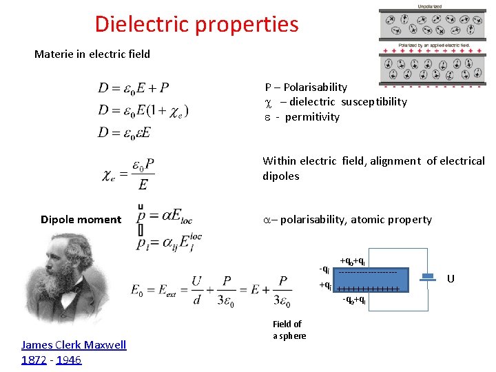
Dielectric properties Materie in electric field P – Polarisability c – dielectric susceptibility e - permitivity Within electric field, alignment of electrical dipoles Dipole moment a– polarisability, atomic property +q 0+qi ----------+qi +++++++ -q 0+qi James Clerk Maxwell 1872 - 1946 Field of a sphere U

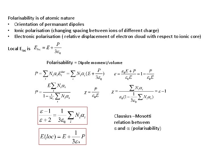
Polarisability is of atomic nature • Orientation of permanant dipoles • Ionic polarisation (changing spacing between ions of different charge) • Electronic polarisation ( relative displacement of electron cloud with respect to ionic core) Local Eloc is Polarisability = Dipole moment/volume Clausius –Mosotti relation between e and a (polarisability)

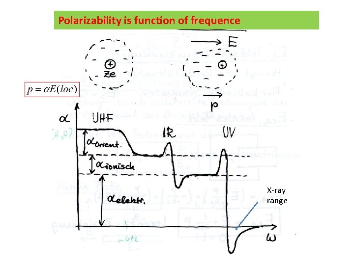
Polarizability is function of frequence X-ray range

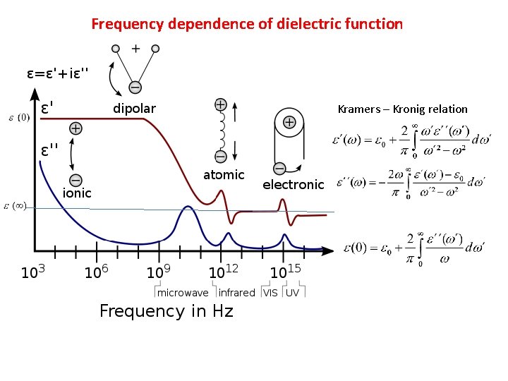
Frequency dependence of dielectric function Kramers – Kronig relation

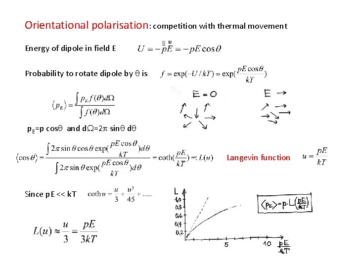
Orientational polarisation: competition with thermal movement Energy of dipole in field E Probability to rotate dipole by q is E p. E=p cosq and d. W=2 p sinq dq Langevin function Since p. E << k. T

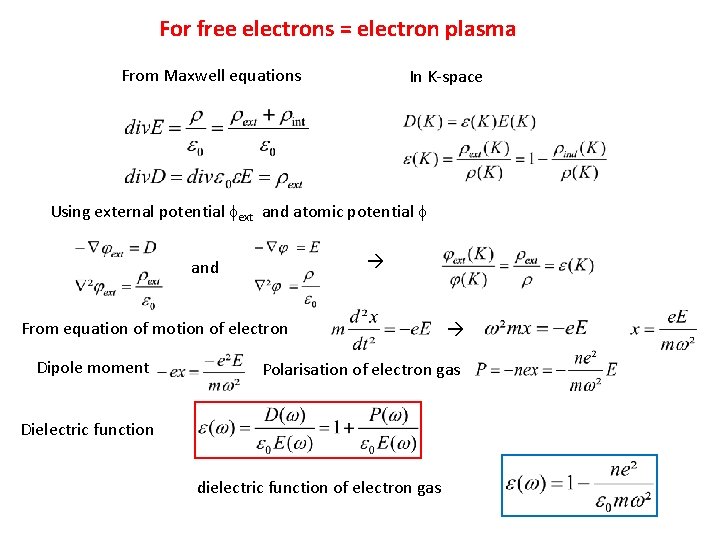
For free electrons = electron plasma From Maxwell equations In K-space Using external potential fext and atomic potential f and From equation of motion of electron Dipole moment Polarisation of electron gas Dielectric function dielectric function of electron gas

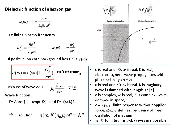
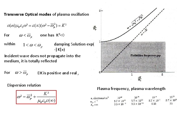
Dielectric function of electron gas Defining plasma frequency If positive ion core background has DK is e=0 at w=wp Because of wave equ. Wave function: E= A exp(-iwt)exp(i. Kr) and D=e(w, K)E solution • e is real and >0, w is real, K is real, electromagnetic wave propageates with phase velocity c/e^ ½ • e is real and <0, w is real, K is inaginary, wave is damped with length 1/|K| • e is complex, w is real, K is complex, wave damped in space, • e= , finite response without applied force, e(w, K) defines frequency of free oscillation of medium • e =0, longitudinal pol. waves are possible

Transverse Optical modes of plasma oscillation For one has K²<0 within damping Solution exp( -|K|x) Incident wave does not propagate into the medium, it is totally reflected For DK is positive and real , Dispersion relation Plasma frequency, plasma wavelength

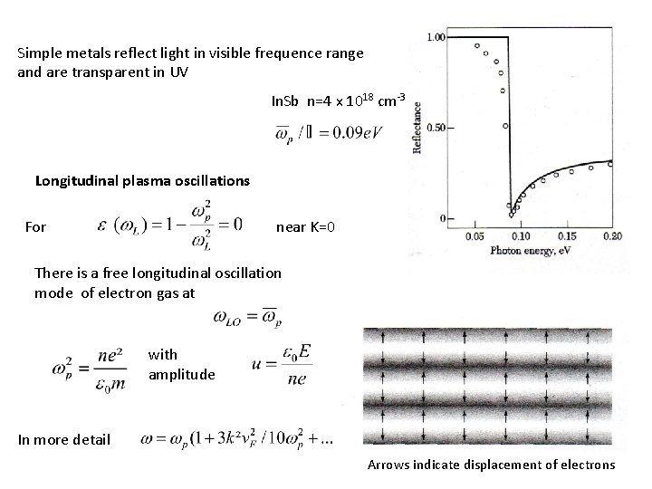
Simple metals reflect light in visible frequence range and are transparent in UV In. Sb n=4 x 1018 cm-3 Longitudinal plasma oscillations For near K=0 There is a free longitudinal oscillation mode of electron gas at with amplitude In more detail Arrows indicate displacement of electrons

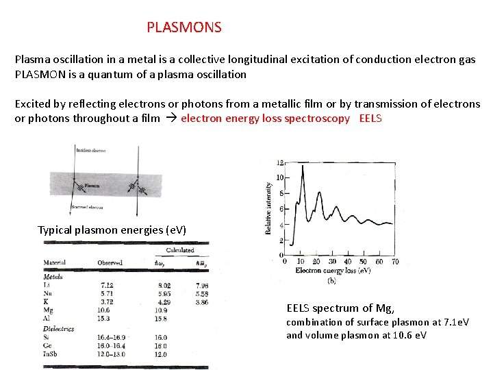
PLASMONS Plasma oscillation in a metal is a collective longitudinal excitation of conduction electron gas PLASMON is a quantum of a plasma oscillation Excited by reflecting electrons or photons from a metallic film or by transmission of electrons or photons throughout a film electron energy loss spectroscopy EELS Typical plasmon energies (e. V) EELS spectrum of Mg, combination of surface plasmon at 7. 1 e. V and volume plasmon at 10. 6 e. V

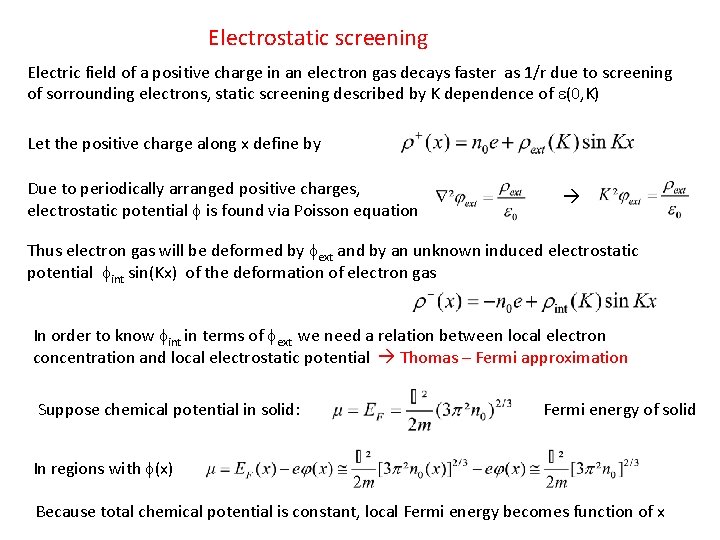
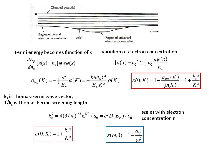
Electrostatic screening Electric field of a positive charge in an electron gas decays faster as 1/r due to screening of sorrounding electrons, static screening described by K dependence of e(0, K) Let the positive charge along x define by Due to periodically arranged positive charges, electrostatic potential f is found via Poisson equation Thus electron gas will be deformed by fext and by an unknown induced electrostatic potential fint sin(Kx) of the deformation of electron gas In order to know fint in terms of fext we need a relation between local electron concentration and local electrostatic potential Thomas – Fermi approximation Suppose chemical potential in solid: Fermi energy of solid In regions with f(x) Because total chemical potential is constant, local Fermi energy becomes function of x

Fermi energy becomes function of x Variation of electron concentration ks is Thomas-Fermi wave vector; 1/ks is Thomas-Fermi screening length scales with electron concentration n

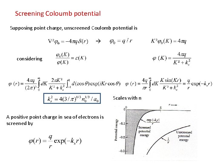
Screening Coloumb potential Supposing point charge, unscreened Coulomb potential is considering Scales with n A positive point charge in sea of electrons is screened by

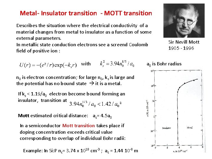
Metal- Insulator transition - MOTT transition Describes the situation where the electrical conductivity of a material changes from metal to insulator as a function of some external parameters. In metallic state conduction electrons see a screend Coulomb field of positive ion : with n 0 is electron concentration; for large n 0, ks is large and the potential has no bound state it is a metal. If ks < 1. 19/a 0 electron become bound forming an insulator, transition at Mott estimated critical distance: ac= 4. 5 a 0 In a semiconductor Mott transition takes place if doping concentration exceeds critical value corresponding to overlap of individual Bohr radii: Example: In Si: P nc= 3. 74 x 1018 cm-3 ; ac = 1. 44 10 -8 m Sir Nevill Mott 1905 - 1996 a 0 is Bohr radius

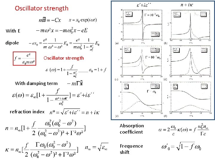
Oscillator strength With E dipole Oscillator strength With damping term refraction index Absorption coefficient Frequence shift

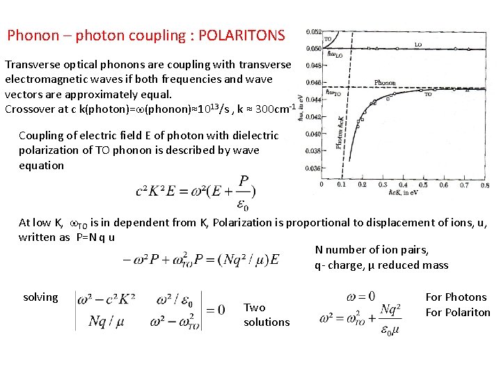
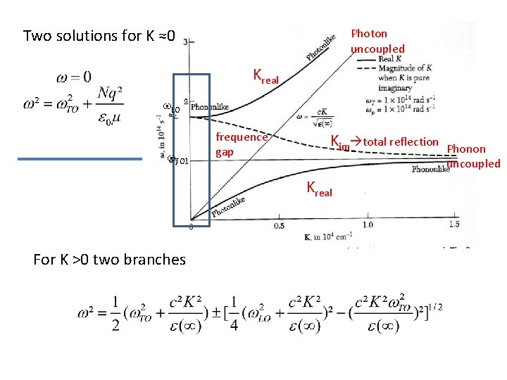
Phonon – photon coupling : POLARITONS Transverse optical phonons are coupling with transverse electromagnetic waves if both frequencies and wave vectors are approximately equal. Crossover at c k(photon)=w(phonon)≈1013/s , k ≈ 300 cm-1 Coupling of electric field E of photon with dielectric polarization of TO phonon is described by wave equation At low K, w. TO is in dependent from K, Polarization is proportional to displacement of ions, u, written as P=N q u N number of ion pairs, q- charge, µ reduced mass solving Two solutions For Photons For Polariton

Two solutions for K ≈0 Photon uncoupled Kreal w. LO w. TO frequence gap Kim total reflection Kreal For K >0 two branches Phonon uncoupled

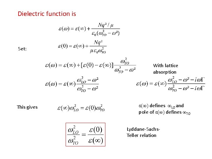
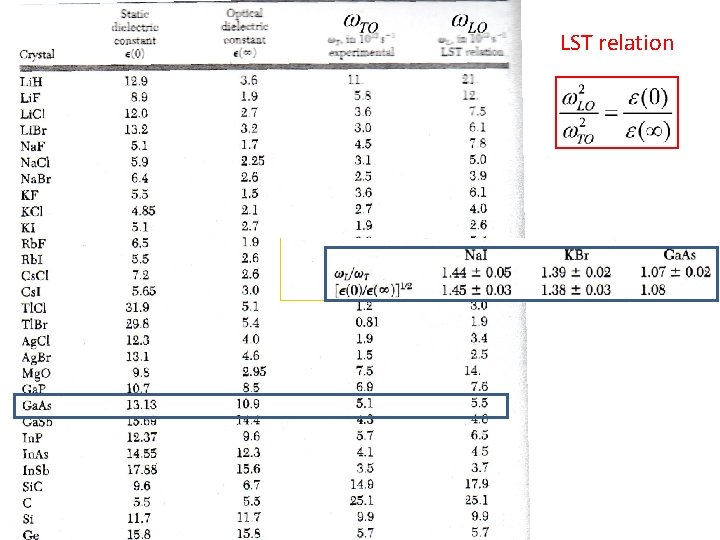
Dielectric function is Set: With lattice absorption This gives e(w) defines w. LO and pole of e(w) defines w. TO Lyddane-Sachs. Teller relation

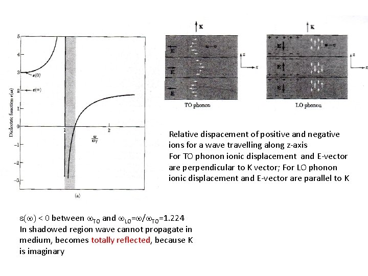
Relative dispacement of positive and negative ions for a wave travelling along z-axis For TO phonon ionic displacement and E-vector are perpendicular to K vector; For LO phonon ionic displacement and E-vector are parallel to K e(w) < 0 between w. TO and w. LO=w/w. TO=1. 224 In shadowed region wave cannot propagate in medium, becomes totally reflected, because K is imaginary

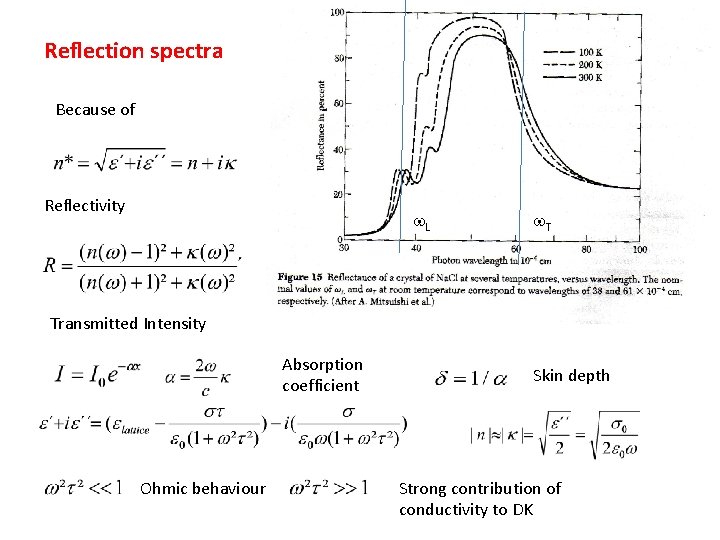
Reflection spectra Because of Reflectivity w. L w. T Transmitted Intensity Absorption coefficient Ohmic behaviour Skin depth Strong contribution of conductivity to DK

LST relation

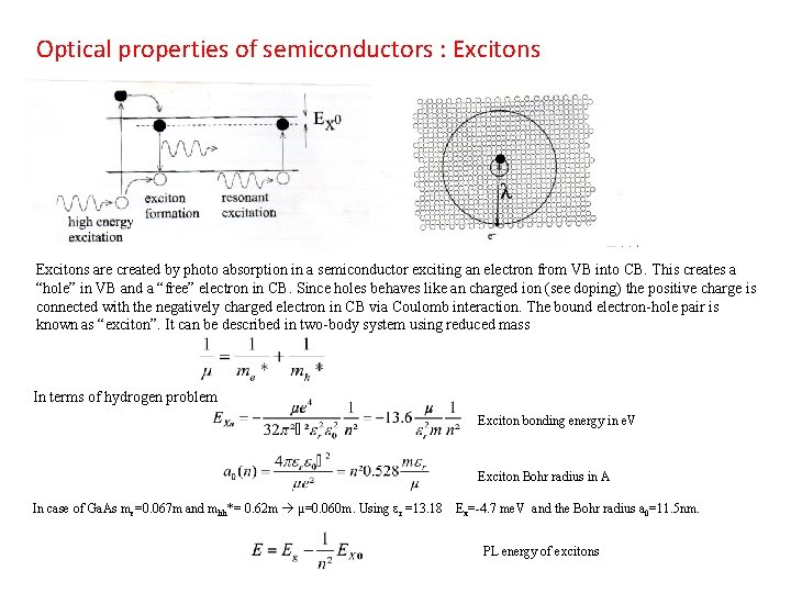
Optical properties of semiconductors : Excitons are created by photo absorption in a semiconductor exciting an electron from VB into CB. This creates a “hole” in VB and a “free” electron in CB. Since holes behaves like an charged ion (see doping) the positive charge is connected with the negatively charged electron in CB via Coulomb interaction. The bound electron-hole pair is known as “exciton”. It can be described in two-body system using reduced mass In terms of hydrogen problem Exciton bonding energy in e. V Exciton Bohr radius in A In case of Ga. As me=0. 067 m and mhh*= 0. 62 m µ=0. 060 m. Using er =13. 18 Ex=-4. 7 me. V and the Bohr radius a 0=11. 5 nm. PL energy of excitons

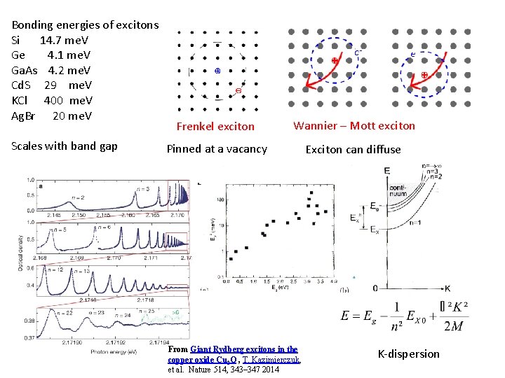
Bonding energies of excitons Si 14. 7 me. V Ge 4. 1 me. V Ga. As 4. 2 me. V Cd. S 29 me. V KCl 400 me. V Ag. Br 20 me. V Scales with band gap Frenkel exciton Wannier – Mott exciton Pinned at a vacancy Exciton can diffuse From Giant Rydberg excitons in the copper oxide Cu 2 O , T. Kazimierczuk, et al. Nature 514, 343– 347 2014 K-dispersion
![EHD Free exciton Electron Hole Droplet hn me V Under illumination and at EHD Free exciton Electron – Hole Droplet hn [me. V] Under illumination and at](https://slidetodoc.com/presentation_image_h/2f97e2503c6e8153006764d3859d4552/image-25.jpg)
EHD Free exciton Electron – Hole Droplet hn [me. V] Under illumination and at low temperatures SC can create an electron – hole droplet. After formation excitons decay into electron- hole pairs which condense to EHD In 1 st approx. electrons and holes move like a twocomponent ideal gas (plasma). Properties are determined by m* and er. In more details they move as in a „liquid“. Mean pair density/cm³

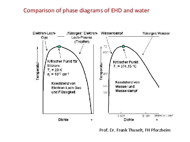
Comparison of phase diagrams of EHD and water Prof. Dr. Frank Thuselt, FH Pforzheim

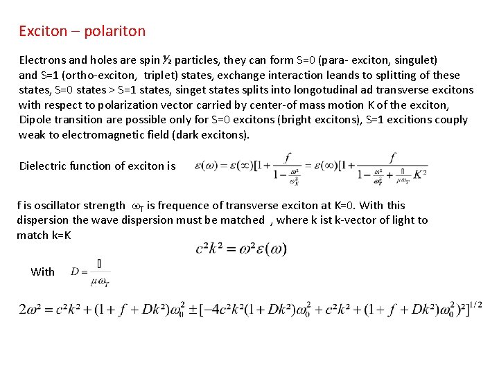
Exciton – polariton Electrons and holes are spin ½ particles, they can form S=0 (para- exciton, singulet) and S=1 (ortho-exciton, triplet) states, exchange interaction leands to splitting of these states, S=0 states > S=1 states, singet states splits into longotudinal ad transverse excitons with respect to polarization vector carried by center-of mass motion K of the exciton, Dipole transition are possible only for S=0 excitons (bright excitons), S=1 excitions couply weak to electromagnetic field (dark excitons). Dielectric function of exciton is f is oscillator strength w. T is frequence of transverse exciton at K=0. With this dispersion the wave dispersion must be matched , where k ist k-vector of light to match k=K With

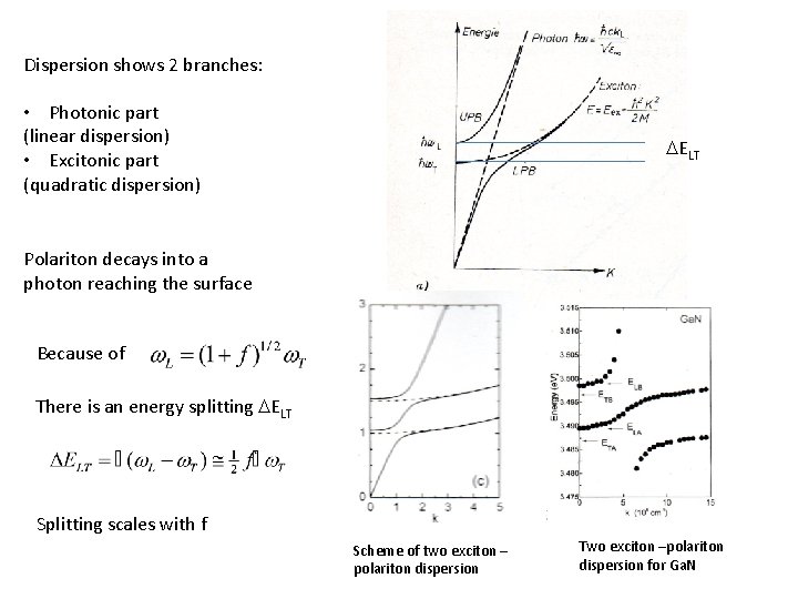
Dispersion shows 2 branches: • Photonic part (linear dispersion) • Excitonic part (quadratic dispersion) DELT Polariton decays into a photon reaching the surface Because of There is an energy splitting DELT Splitting scales with f Scheme of two exciton – polariton dispersion Two exciton –polariton dispersion for Ga. N

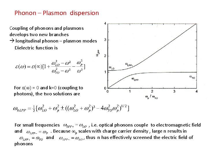
Phonon – Plasmon dispersion Coupling of phonons and plasmons develops two new branches longitudinal phonon – plasmon modes Dielectric function is For e(w) = 0 and k=0 (coupling to photons), the two solutions are For small frequencies , i. e. optical phonons couple to electromagnetic field and. Because wp scales with charge carrier density , large n results in and , thus n has effectively screened the electric field of phonons