Solid State Electronics EC 210 EC 211 Prof


")
 unit cell contains: 1 • 8 x 1/8 =1 atom/unit cell.")
 Each corner atom is shared among 8 unit cells 1/8")

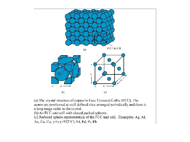
 Face-centered atoms only belong to two unit cells 1/2 atom")


 surface of a single crystal silicon")

- Slides: 18
Solid State Electronics EC 210 – EC 211 Prof. Dr. Iman Gamal Eldin Morsi 1
Crystal Structures Cubic Fe. S 2, iron sulfide, or pyrite, crystals. The crystals look brass-like yellow (“fool’s gold”). Galena is lead sulfide, Pb. S, and has a cubic crystal structure |SOURCE: Photo by SOK
Chapter 1: Crystal Structure 3
Classification of solids according to the arrangement of atoms: Crystalline atoms pack in periodic, 3 D arrays • typical of: -metals • many ceramicssome polymers- (Noncrystalline (amorphous atoms have no periodic packing • : occurs for • complex structuresrapid cooling- 4
Lattice and Unit cell: • Lattice- an in definitely extended arrangement of points each of which is surrounded by an identical grouping of neighboring point • Unit cell - smallest region that completely describes the pattern 5
Types of Unit Cell 6
Types of Cubic Unit Cell: Crystals with same type of atom: Simple Cubic (SC) Body-Centered Cubic (BCC) Face-Center Cubic (FCC) Diamond unit cell Crystals with multiple atoms: Zinc Blend unit cell NACl unit cell 7 • •
Simple Cubic (SC) unit cell contains: 1 • 8 x 1/8 =1 atom/unit cell. a: lattice parameter • R: atomic radius • a=2 R 8
Body Centered Cubic (BCC) Each corner atom is shared among 8 unit cells 1/8 atom at each corner • 1 atom at the center. • 1 Unit cell contains: • 1 + 8 x 1/8 = 2 atoms/unit cell. 4 R = Diagonals of the cube 9
Fig 1. 32
Face Centered Cubic (FCC) Face-centered atoms only belong to two unit cells 1/2 atom at the center of each face. • 1/8 atom at each corner. • 1 Unit cell contains: • ½ x 6 + 8 x ⅛= 4 atoms/unit cell. Diagonals of the face (square) 11
Fig 1. 39
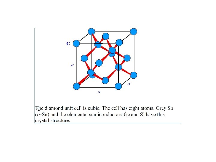
Diamond unit cell 1/2 atom at the center of each face. • 1/8 atom at each corner. • 1 atom at the quarter of each • diagonal. (there are 4 diagonals for the cube) 1 Unit cell contains: • ½ x 6 + 8 x ⅛ + 4= 8 atoms/unit cell. = 8 R 14
Silicon A silicon ingot is a single crystal of Si. Within the bulk of the crystal, the atoms are arranged on a well-defined periodical lattice. The crystal structure is that of diamond. |Courtesy of MEMC, Electronic Materials Inc.
Left: A polycrystalline diamond film on the (100) surface of a single crystal silicon wafer. The film thickness is 6 microns and the SEM magnification is 6000. Right: A 6 -micron-thick CVD diamond film grown on a single crystal silicon wafer. SEM magnification is 8000.
Fig 1. 43