SOLAR ENERGY The average solar power incident on
- Slides: 12

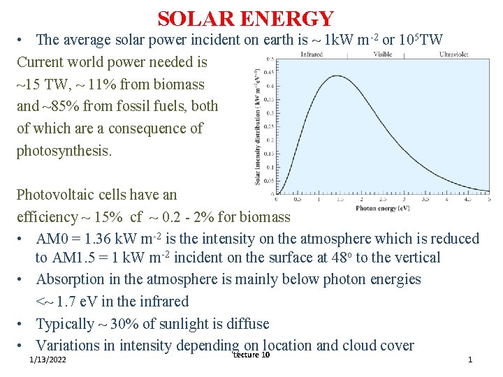
SOLAR ENERGY • The average solar power incident on earth is ~ 1 k. W m-2 or 105 TW Current world power needed is ~15 TW, ~ 11% from biomass and ~85% from fossil fuels, both of which are a consequence of photosynthesis. Photovoltaic cells have an efficiency ~ 15% cf ~ 0. 2 - 2% for biomass • AM 0 = 1. 36 k. W m-2 is the intensity on the atmosphere which is reduced to AM 1. 5 = 1 k. W m-2 incident on the surface at 48 o to the vertical • Absorption in the atmosphere is mainly below photon energies <~ 1. 7 e. V in the infrared • Typically ~ 30% of sunlight is diffuse • Variations in intensity depending. Lecture on 10 location and cloud cover 1/13/2022 1

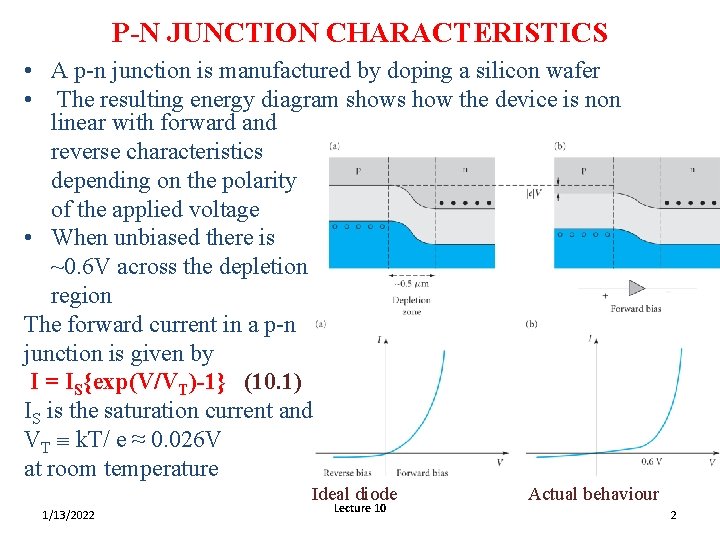
P-N JUNCTION CHARACTERISTICS • A p-n junction is manufactured by doping a silicon wafer • The resulting energy diagram shows how the device is non linear with forward and reverse characteristics depending on the polarity of the applied voltage • When unbiased there is ~0. 6 V across the depletion region The forward current in a p-n junction is given by I = IS{exp(V/VT)-1} (10. 1) IS is the saturation current and VT k. T/ e ≈ 0. 026 V at room temperature Ideal diode 1/13/2022 Lecture 10 Actual behaviour 2

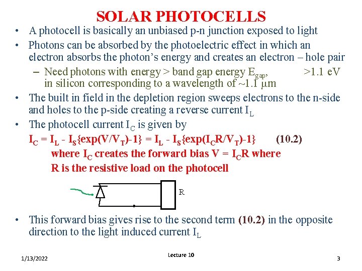
SOLAR PHOTOCELLS • A photocell is basically an unbiased p-n junction exposed to light • Photons can be absorbed by the photoelectric effect in which an electron absorbs the photon’s energy and creates an electron – hole pair – Need photons with energy > band gap energy Egap, >1. 1 e. V in silicon corresponding to a wavelength of ~1. 1 mm • The built in field in the depletion region sweeps electrons to the n-side and holes to the p-side creating a reverse current IL • The photocell current IC is given by IC = IL - IS{exp(V/VT)-1} = IL - IS{exp(ICR/VT)-1} (10. 2) where IC creates the forward bias V = ICR where R is the resistive load on the photocell R • This forward bias gives rise to the second term (10. 2) in the opposite direction to the light induced current IL 1/13/2022 Lecture 10 3

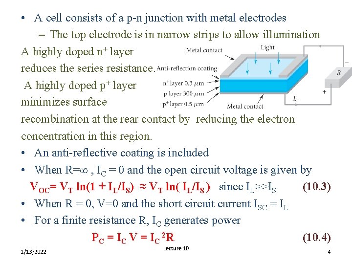
• A cell consists of a p-n junction with metal electrodes – The top electrode is in narrow strips to allow illumination A highly doped n+ layer reduces the series resistance. A highly doped p+ layer minimizes surface recombination at the rear contact by reducing the electron concentration in this region. • An anti-reflective coating is included • When R=∞ , IC = 0 and the open circuit voltage is given by VOC= VT ln(1 + IL/IS) ≈ VT ln( IL/IS ) since IL>>IS (10. 3) • When R = 0, V=0 and the short circuit current ISC = IL • For a finite resistance R, IC generates power P C = I C V = I C 2 R (10. 4) 1/13/2022 Lecture 10 4

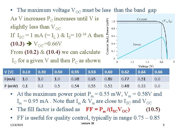
• The maximum voltage VOC must be less than the band gap As V increases PC increases until V is slightly less than VOC If ISC = 1 m. A (= IL ) & IS= 10 -14 A then (10. 3) VOC =0. 66 V From (10. 2) & (10. 4) we can calculate IC for a given V and then PC as shown V (V) 0. 10 0. 30 0. 55 0. 58 0. 60 0. 62 0. 64 0. 66 I (m. A) 1. 0 0. 98 0. 95 0. 89 0. 77 0. 51 0. 0 P (m. W) 0. 1 0. 3 0. 54 0. 55 0. 53 0. 48 0. 33 0. 0 • At the maximum power point Pm = 0. 55 m. W, Vm = 0. 58 V and Im = 0. 95 m. A. Note that Im & Vm are close to ISC and VOC • The fill factor is defined as FF = Pm /(ISCVOC) (10. 5) • FF is useful for quality control, typically in range 0. 75 – 0. 85 1/13/2022 Lecture 10 5

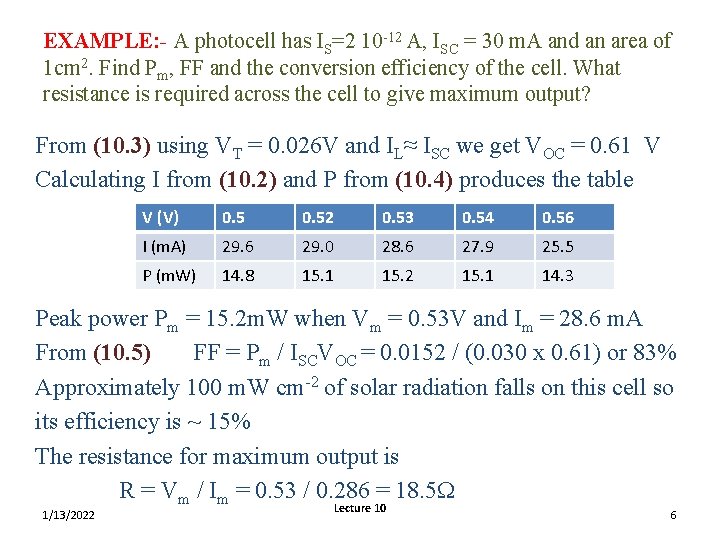
EXAMPLE: - A photocell has IS=2 10 -12 A, ISC = 30 m. A and an area of 1 cm 2. Find Pm, FF and the conversion efficiency of the cell. What resistance is required across the cell to give maximum output? From (10. 3) using VT = 0. 026 V and IL≈ ISC we get VOC = 0. 61 V Calculating I from (10. 2) and P from (10. 4) produces the table V (V) 0. 52 0. 53 0. 54 0. 56 I (m. A) 29. 6 29. 0 28. 6 27. 9 25. 5 P (m. W) 14. 8 15. 1 15. 2 15. 1 14. 3 Peak power Pm = 15. 2 m. W when Vm = 0. 53 V and Im = 28. 6 m. A From (10. 5) FF = Pm / ISCVOC = 0. 0152 / (0. 030 x 0. 61) or 83% Approximately 100 m. W cm-2 of solar radiation falls on this cell so its efficiency is ~ 15% The resistance for maximum output is R = Vm / Im = 0. 53 / 0. 286 = 18. 5 W 1/13/2022 Lecture 10 6

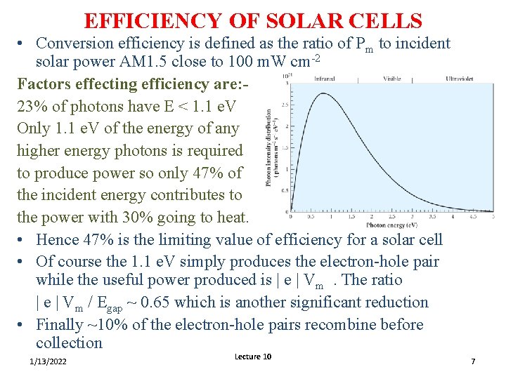
EFFICIENCY OF SOLAR CELLS • Conversion efficiency is defined as the ratio of Pm to incident solar power AM 1. 5 close to 100 m. W cm-2 Factors effecting efficiency are: 23% of photons have E < 1. 1 e. V Only 1. 1 e. V of the energy of any higher energy photons is required to produce power so only 47% of the incident energy contributes to the power with 30% going to heat. • Hence 47% is the limiting value of efficiency for a solar cell • Of course the 1. 1 e. V simply produces the electron-hole pair while the useful power produced is | e | Vm. The ratio | e | Vm / Egap ~ 0. 65 which is another significant reduction • Finally ~10% of the electron-hole pairs recombine before collection 1/13/2022 Lecture 10 7

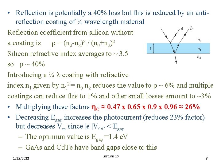
• Reflection is potentially a 40% loss but this is reduced by an antireflection coating of ¼ wavelength material Reflection coefficient from silicon without a coating is r = (n 0 -n 2)2 / (n 0+n 2)2 Silicon refractive index averages to ~ 3. 5 so r ~ 40% Introducing a ¼ l coating with refractive index n 1 given by n 12 = n 0 n 2 reduces the value to r ~ 6% and multiple coatings can reduce this to 1% and other small losses amount to ~3% • Multiplying these factors h. C ≈ 0. 47 x 0. 65 x 0. 96 ≈ 26% • Decreasing Egap increases the photocurrent (reduces 23% factor) but decreases Vm since |e |VOC < Egap – The optimum value is Egap =1. 4 e. V – Ga. As and Cd. Te have band gaps close to this 1/13/2022 Lecture 10 8

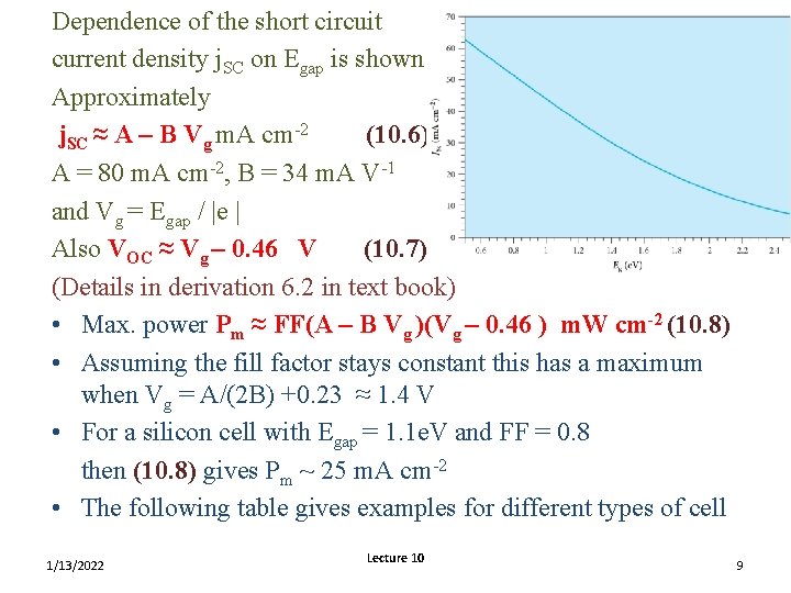
Dependence of the short circuit current density j. SC on Egap is shown Approximately j. SC ≈ A – B Vg m. A cm-2 (10. 6) A = 80 m. A cm-2, B = 34 m. A V-1 and Vg = Egap / |e | Also VOC ≈ Vg – 0. 46 V (10. 7) (Details in derivation 6. 2 in text book) • Max. power Pm ≈ FF(A – B Vg )(Vg – 0. 46 ) m. W cm-2 (10. 8) • Assuming the fill factor stays constant this has a maximum when Vg = A/(2 B) +0. 23 ≈ 1. 4 V • For a silicon cell with Egap = 1. 1 e. V and FF = 0. 8 then (10. 8) gives Pm ~ 25 m. A cm-2 • The following table gives examples for different types of cell 1/13/2022 Lecture 10 9

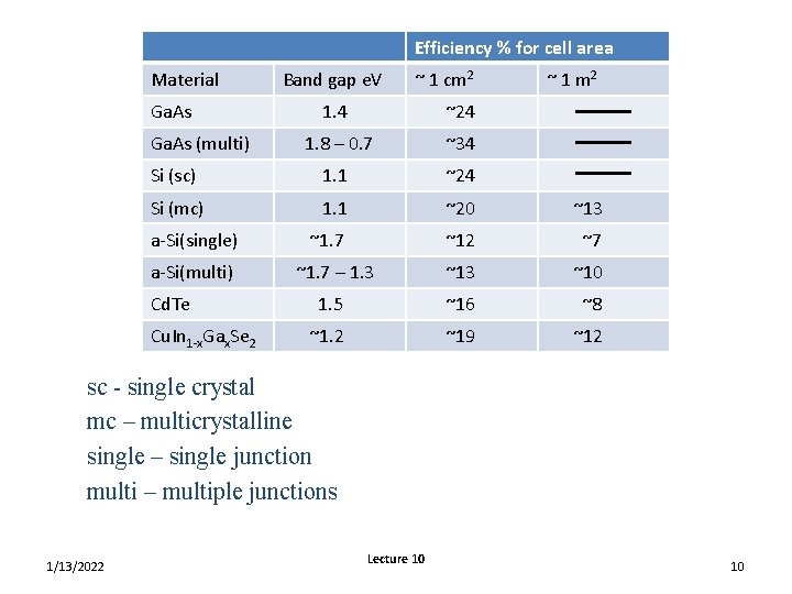
Efficiency % for cell area Material Ga. As Band gap e. V ~ 1 cm 2 ~ 1 m 2 1. 4 ~24 1. 8 – 0. 7 ~34 Si (sc) 1. 1 ~24 Si (mc) 1. 1 ~20 ~13 ~1. 7 ~12 ~7 ~1. 7 – 1. 3 ~10 1. 5 ~16 ~8 ~1. 2 ~19 ~12 Ga. As (multi) a-Si(single) a-Si(multi) Cd. Te Cu. In 1 -x. Gax. Se 2 sc - single crystal mc – multicrystalline single – single junction multi – multiple junctions 1/13/2022 Lecture 10 10

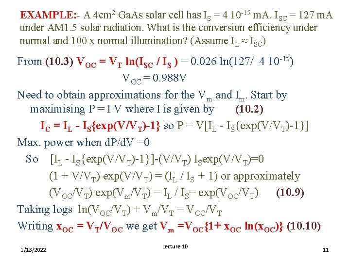
EXAMPLE: - A 4 cm 2 Ga. As solar cell has IS = 4 10 -15 m. A. ISC = 127 m. A under AM 1. 5 solar radiation. What is the conversion efficiency under normal and 100 x normal illumination? (Assume IL ≈ ISC) From (10. 3) VOC = VT ln(ISC / IS ) = 0. 026 ln(127/ 4 10 -15) VOC = 0. 988 V Need to obtain approximations for the Vm and Im. Start by maximising P = I V where I is given by (10. 2) IC = IL - IS{exp(V/VT)-1} so P = V[IL - IS{exp(V/VT)-1}] Max. power when d. P/d. V =0 So [IL - IS{exp(V/VT)-1}]-(V/VT) ISexp(V/VT)=0 (1 + V/VT) exp(V/VT) = (IL / IS + 1) or approximately (VOC/VT) exp(Vm/VT) = IL / IS= exp(VOC/VT) (10. 9) Taking logs ln(VOC/VT) + Vm/VT = VOC/VT Writing x. OC = VT/VOC we get Vm =VOC{1+ x. OC ln(x. OC)} (10. 10) 1/13/2022 Lecture 10 11

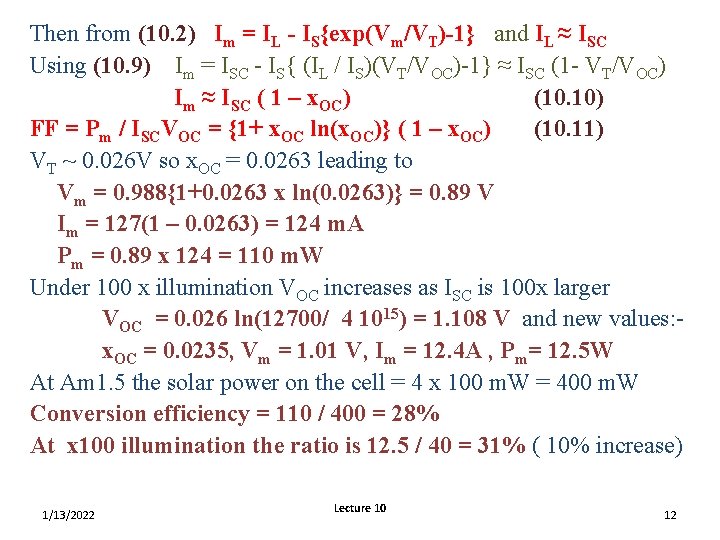
Then from (10. 2) Im = IL - IS{exp(Vm/VT)-1} and IL ≈ ISC Using (10. 9) Im = ISC - IS{ (IL / IS)(VT/VOC)-1} ≈ ISC (1 - VT/VOC) Im ≈ ISC ( 1 – x. OC) (10. 10) FF = Pm / ISCVOC = {1+ x. OC ln(x. OC)} ( 1 – x. OC) (10. 11) VT ~ 0. 026 V so x. OC = 0. 0263 leading to Vm = 0. 988{1+0. 0263 x ln(0. 0263)} = 0. 89 V Im = 127(1 – 0. 0263) = 124 m. A Pm = 0. 89 x 124 = 110 m. W Under 100 x illumination VOC increases as ISC is 100 x larger VOC = 0. 026 ln(12700/ 4 1015) = 1. 108 V and new values: x. OC = 0. 0235, Vm = 1. 01 V, Im = 12. 4 A , Pm= 12. 5 W At Am 1. 5 the solar power on the cell = 4 x 100 m. W = 400 m. W Conversion efficiency = 110 / 400 = 28% At x 100 illumination the ratio is 12. 5 / 40 = 31% ( 10% increase) 1/13/2022 Lecture 10 12