
Solar Cells An Overview Onkar S Game Senior







- Slides: 40
Solar Cells: An Overview Onkar S. Game Senior Research Fellow, National Chemical Laboratory, Pune.
Outline • Introduction: Need for harnessing solar energy • Historical development of modern photovoltaic effect: Example of p-n junction • Thin Film Solar Cells: Examples • Modern Solar Cells: Nanotechnology and Polymers • Current Status and Future Prospective
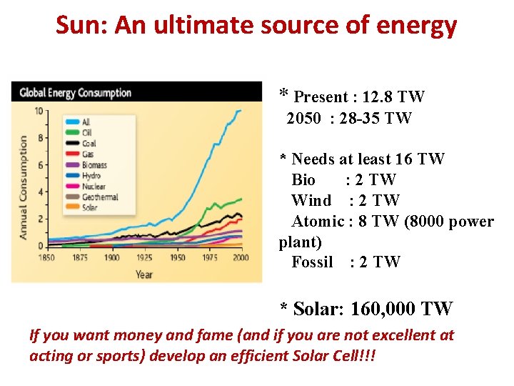
Sun: An ultimate source of energy * Present : 12. 8 TW 2050 : 28 -35 TW * Needs at least 16 TW Bio : 2 TW Wind : 2 TW Atomic : 8 TW (8000 power plant) Fossil : 2 TW * Solar: 160, 000 TW If you want money and fame (and if you are not excellent at acting or sports) develop an efficient Solar Cell!!!
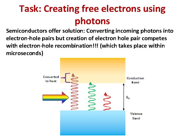
Task: Creating free electrons using photons Semiconductors offer solution: Converting incoming photons into electron-hole pairs but creation of electron hole pair competes with electron-hole recombination!!! (which takes place within microseconds)
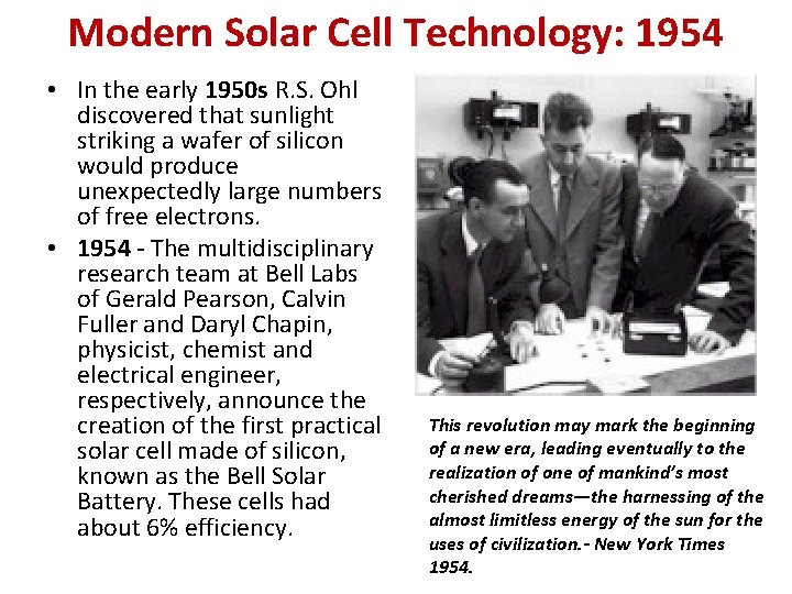
Modern Solar Cell Technology: 1954 • In the early 1950 s R. S. Ohl discovered that sunlight striking a wafer of silicon would produce unexpectedly large numbers of free electrons. • 1954 - The multidisciplinary research team at Bell Labs of Gerald Pearson, Calvin Fuller and Daryl Chapin, physicist, chemist and electrical engineer, respectively, announce the creation of the first practical solar cell made of silicon, known as the Bell Solar Battery. These cells had about 6% efficiency. This revolution may mark the beginning of a new era, leading eventually to the realization of one of mankind’s most cherished dreams—the harnessing of the almost limitless energy of the sun for the uses of civilization. - New York Times 1954.
Silicon Solar Cell Schematic Why thickness of p type and n type semiconductor layers are different?
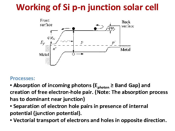
Working of Si p-n junction solar cell Processes: • Absorption of incoming photons (Ephoton ≥ Band Gap) and creation of free electron-hole pair. (Note: The absorption process has to dominant near junction) • Separation of electron hole pairs in presence of internal potential (junction potential). • Vectorial transport of electrons and holes in opposite direction.
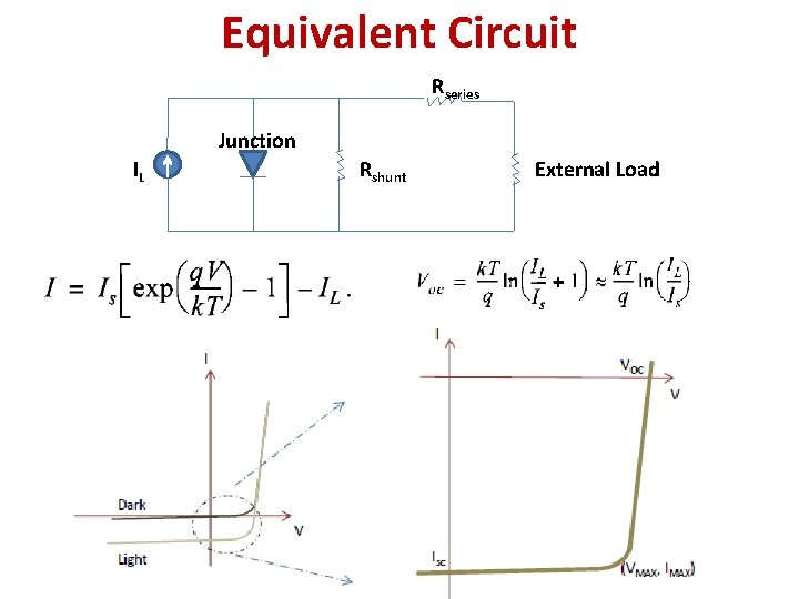
Equivalent Circuit Rseries Junction IL Rshunt External Load
Parameters that characterize solar cell IV curve • Voc: Open Circuit Voltage • Isc : Short Circuit Current • Pmax: Maximum Power Delivered • Vm: Voltage corresponding to Pmax • Im: Current corresponding to Pmax • FF (Fill Factor): • Efficiency = • Series Resistance: (d. I/dv)-1 at Voc • Shunt Resistance: (d. I/dv)-1 at Isc
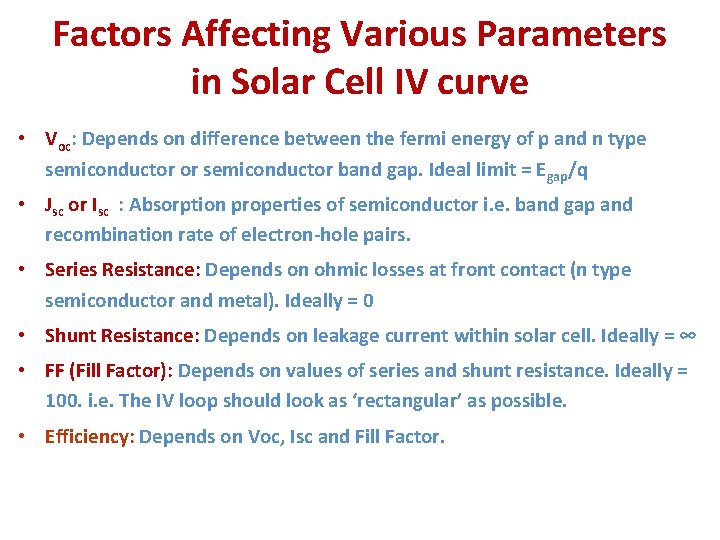
Factors Affecting Various Parameters in Solar Cell IV curve • Voc: Depends on difference between the fermi energy of p and n type semiconductor or semiconductor band gap. Ideal limit = Egap/q • Jsc or Isc : Absorption properties of semiconductor i. e. band gap and recombination rate of electron-hole pairs. • Series Resistance: Depends on ohmic losses at front contact (n type semiconductor and metal). Ideally = 0 • Shunt Resistance: Depends on leakage current within solar cell. Ideally = ∞ • FF (Fill Factor): Depends on values of series and shunt resistance. Ideally = 100. i. e. The IV loop should look as ‘rectangular’ as possible. • Efficiency: Depends on Voc, Isc and Fill Factor.
Solar Cell IV Measurement in Lab Solar Simulator
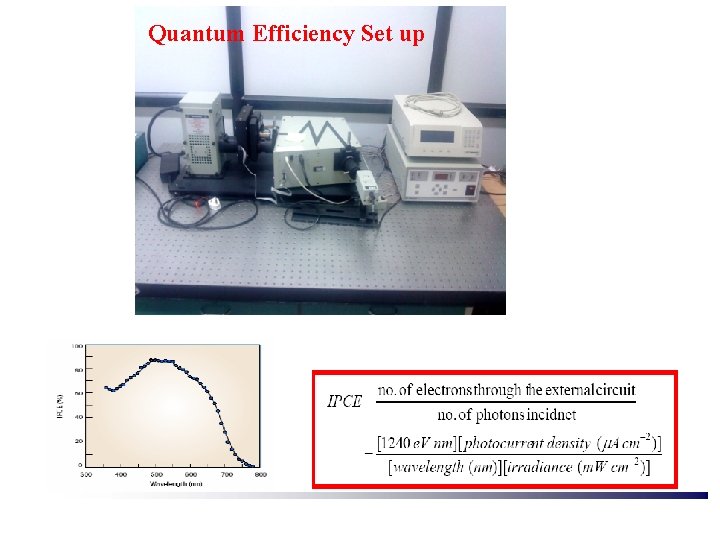
Quantum Efficiency Set up
Current Status of Si Solar Cells Factors Limiting Efficiencies:
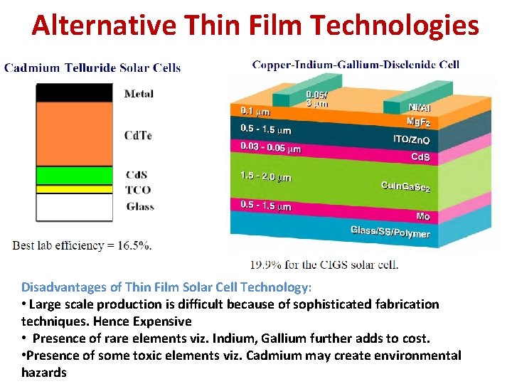
Alternative Thin Film Technologies Disadvantages of Thin Film Solar Cell Technology: • Large scale production is difficult because of sophisticated fabrication techniques. Hence Expensive • Presence of rare elements viz. Indium, Gallium further adds to cost. • Presence of some toxic elements viz. Cadmium may create environmental hazards
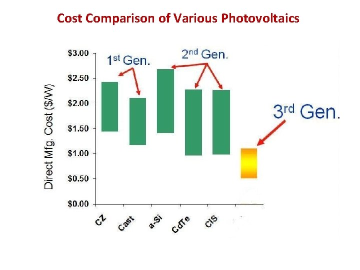
Cost Comparison of Various Photovoltaics
Nanotechnology: Towards low cost solar cells
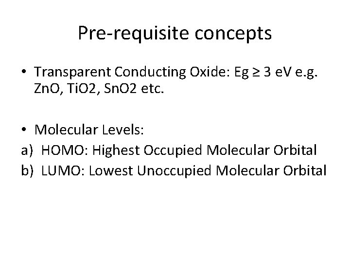
Pre-requisite concepts • Transparent Conducting Oxide: Eg ≥ 3 e. V e. g. Zn. O, Ti. O 2, Sn. O 2 etc. • Molecular Levels: a) HOMO: Highest Occupied Molecular Orbital b) LUMO: Lowest Unoccupied Molecular Orbital
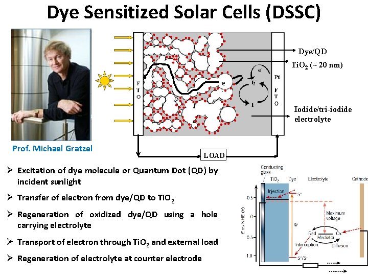
Dye Sensitized Solar Cells (DSSC) Dye/QD Ti. O 2 Ti. O (~(~2020 nm) 2 e - Iodide/tri-iodide electrolyte Prof. Michael Gratzel LOAD Ø Excitation of dye molecule or Quantum Dot (QD) by incident sunlight Ø Transfer of electron from dye/QD to Ti. O 2 Ø Regeneration of oxidized dye/QD using a hole carrying electrolyte Ø Transport of electron through Ti. O 2 and external load Ø Regeneration of electrolyte at counter electrode
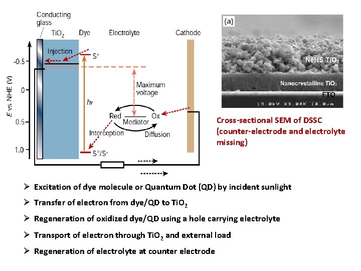
Cross-sectional SEM of DSSC (counter-electrode and electrolyte missing) Ø Excitation of dye molecule or Quantum Dot (QD) by incident sunlight Ø Transfer of electron from dye/QD to Ti. O 2 Ø Regeneration of oxidized dye/QD using a hole carrying electrolyte Ø Transport of electron through Ti. O 2 and external load Ø Regeneration of electrolyte at counter electrode
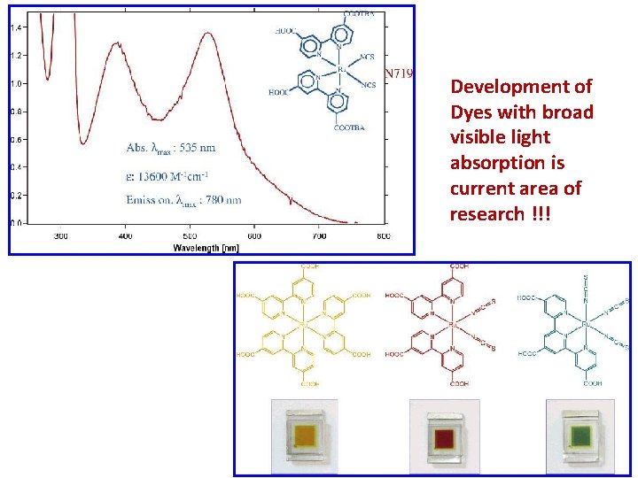
Development of Dyes with broad visible light absorption is current area of research !!!
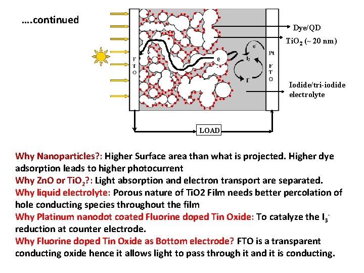
…. continued Dye/QD Ti. O 2 Ti. O (~(~2020 nm) 2 e - Iodide/tri-iodide electrolyte LOAD Why Nanoparticles? : Higher Surface area than what is projected. Higher dye adsorption leads to higher photocurrent Why Zn. O or Ti. O 2? : Light absorption and electron transport are separated. Why liquid electrolyte: Porous nature of Ti. O 2 Film needs better percolation of hole conducting species throughout the film Why Platinum nanodot coated Fluorine doped Tin Oxide: To catalyze the I 3 reduction at counter electrode. Why Fluorine doped Tin Oxide as Bottom electrode? FTO is a transparent conducting oxide hence it allows light to pass through it and it is conducting.
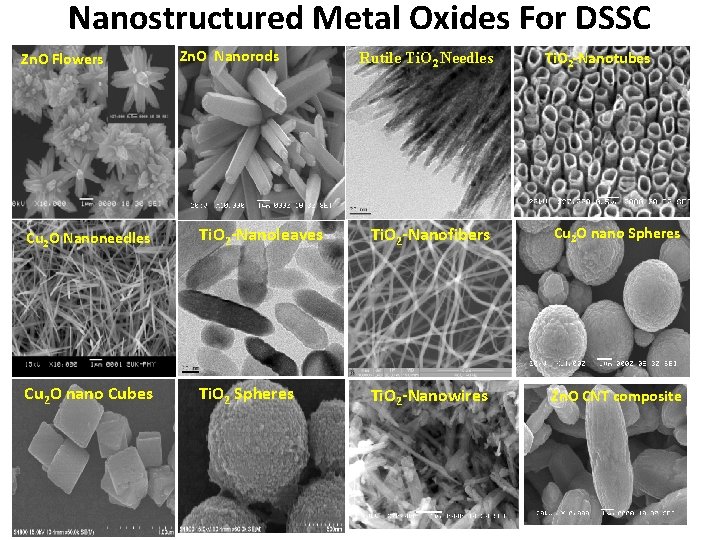
Nanostructured Metal Oxides For DSSC Zn. O Flowers Zn. O Nanorods Rutile Ti. O 2 Needles Ti. O 2 -Nanotubes Cu 2 O Nanoneedles Ti. O 2 -Nanoleaves Ti. O 2 -Nanofibers Cu 2 O nano Spheres Cu 2 O nano Cubes Ti. O 2 Spheres Ti. O 2 -Nanowires Zn. O CNT composite
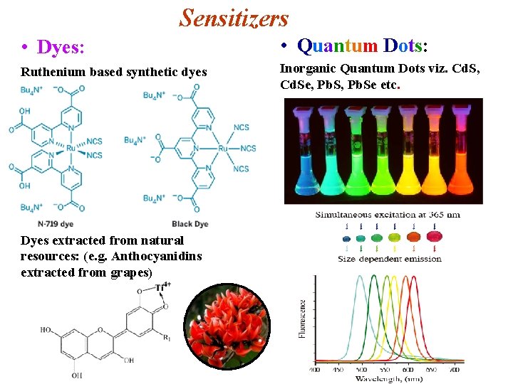
Sensitizers • Dyes: • Quantum Dots: Ruthenium based synthetic dyes Inorganic Quantum Dots viz. Cd. S, Cd. Se, Pb. Se etc. Dyes extracted from natural resources: (e. g. Anthocyanidins extracted from grapes)
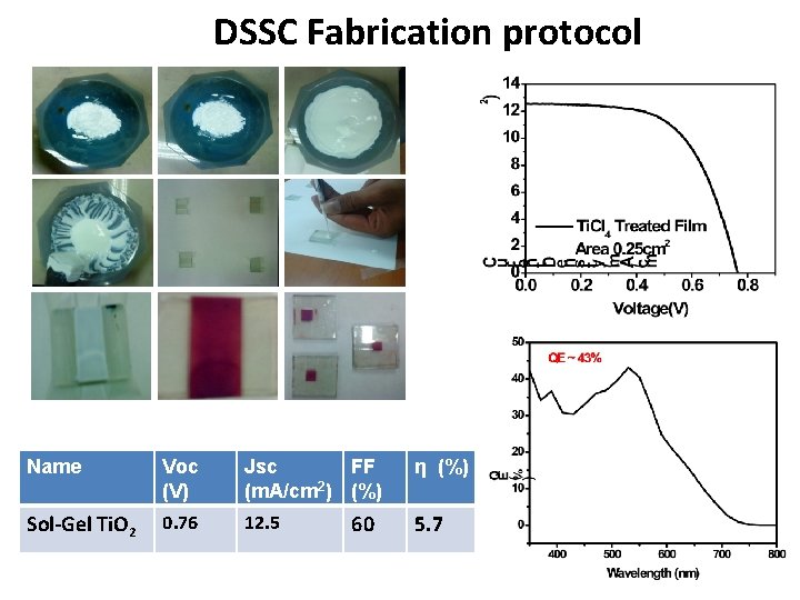
DSSC Fabrication protocol Name Voc (V) Jsc FF (m. A/cm 2) (%) Sol-Gel Ti. O 2 0. 76 12. 5 60 η (%) 5. 7
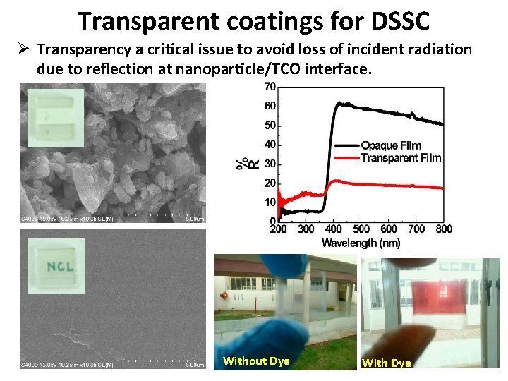
Transparent coatings for DSSC Ø Transparency a critical issue to avoid loss of incident radiation due to reflection at nanoparticle/TCO interface. Without Dye With Dye
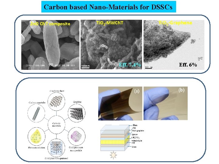
Carbon based Nano-Materials for DSSCs Zn. O CNT composite Ti. O 2 -MWCNT Eff. 7. 4% Ti. O 2 -Graphene Eff. 6%
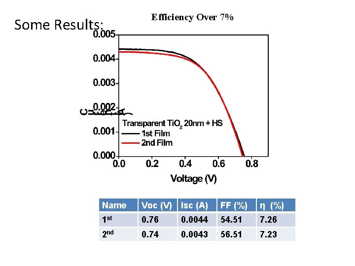
Some Results: Efficiency Over 7% Name Voc (V) Isc (A) FF (%) η (%) 1 st 0. 76 0. 0044 54. 51 7. 26 2 nd 0. 74 0. 0043 56. 51 7. 23
Various Experimental Techniques Used to Characterize DSSC • IV measurement under Solar Simulator • Wavelength Dependant IV measurement: IPCE Setup or Quantum Efficiency Setup • Electrochemical Impedance Spectroscopy: To determine time dynamics in DSSC upto microsecond scale • Transient pump-probe measurement setup: To determine time dynamics in DSSC on nanosecond and picosencond time scale
Current Status of DSSC • Highest Efficiency on small area test cells: 11. 3%. Further increase is a challenge. • Highest efficiency on modules: 9. 2% • Issues related to use of liquid electrolyte and its evaporation. Development of solid state electrolytes. • Development of dyes with enhanced visible light absorption.
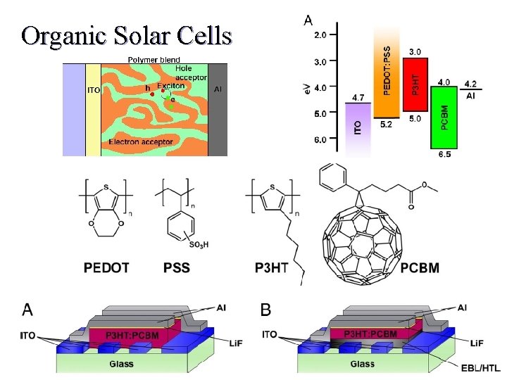
Organic Solar Cells
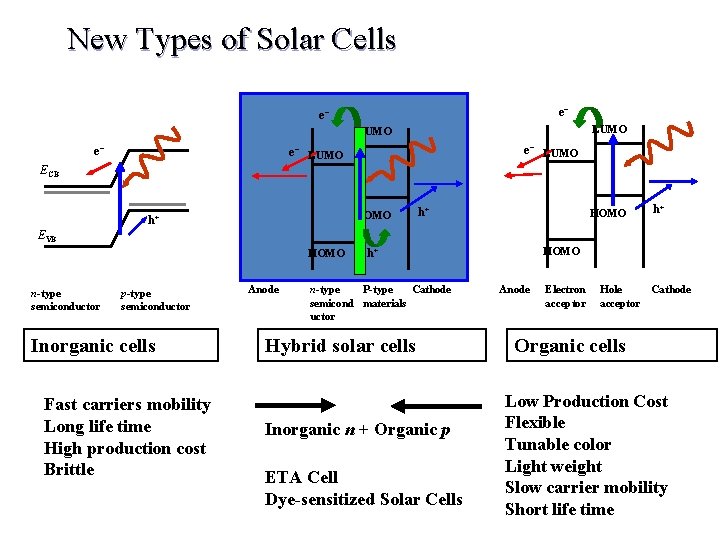
New Types of Solar Cells e– e– LUMO ECB HOMO h+ h+ HOMO h+ EVB HOMO n-type semiconductor p-type semiconductor Inorganic cells Fast carriers mobility Long life time High production cost Brittle Anode HOMO h+ n-type P-type Cathode semicond materials uctor Hybrid solar cells Inorganic n + Organic p ETA Cell Dye-sensitized Solar Cells Anode Electron acceptor Hole acceptor Cathode Organic cells Low Production Cost Flexible Tunable color Light weight Slow carrier mobility Short life time
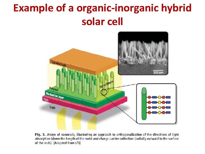
Example of a organic-inorganic hybrid solar cell
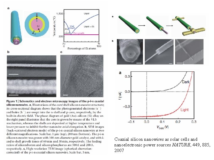
Nano p-n junction solar cells
Coaxial silicon nanowires as solar cells and nanoelectronic power sources NATURE, 449, 885, 2007
Thank You!!!