Solar Cells 1 st developed 1950 Silicon melted

 to use US space satellite Solar")


 cotton, (dry) paper, (dry),")


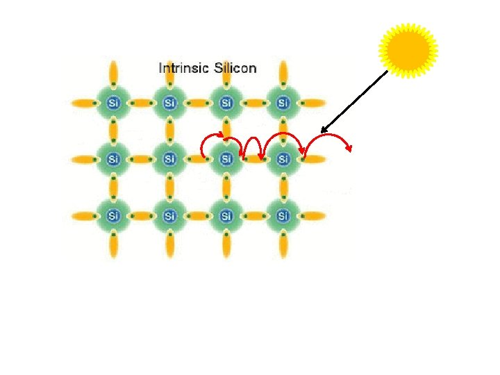
 Continually produce new e- hole pairs How its continually produced? Due")
 +")


 generation by absorption of")
 =hc/λ or E =hv Where, h=planck's constant (6. 62 x")
 like Phosphorous")
 Single Crystal Silicon b) Poly Crystalline & Amorphous Silicon")
 Silicon melting point 1410 o. C")
 Single Crystal Silicon b) Poly Crystalline & Amorphous Silicon")

 Single Crystal Silicon b) Poly Crystalline & Amorphous Silicon")
- Slides: 44
Solar Cells 태 양 전지
1 st developed 1950 Silicon 규소 (melted sand) to use US space satellite Solar cell or PV cell is a device Solar radiation into electricity Two layers of solid chemical element semiconductor Using semiconductor 반도체 Conduct electricity under some conditions Two additive layers Good medium for control of electrical current Photosensitive 민 감한
Photon strike Electron hole pairs released Generate flow of electricity
Solar cells also called Photovoltaic cells or PV Cells Composed of various semi conducting materials 92 to 95% of solar cells Applications Roadside hoarding Composed of silicon semiconductor Calculators Home Amount of electricity Day - maximum Space crafts Night - zero
Light to electricity depends on Reflectivity of the surface Absorptivity of the material Rate of generation & recombination of charge carriers
Solar cell Fundamentals Before understand solar cell, we should know about Atoms 원자 made of Electrons Protons Neutrons 92% silicon What is semiconductor 반도체? How its work?
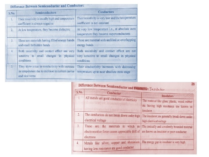
Any solid materials based on electrical conductivity classified into Conductor 도체 Conductivity 전도도 Semiconductor 반도체 Insulator 절연체 Depends on number of e- in the valence 원자가 orbit Valence is outer most orbit
3 valence electrons 5 valence electrons 4 valence electrons 32 p+ 41 n 0 Electron diagram of 3 typical elements Element’s used in semiconductor manufacture Degree of conductivity Good conductor Atoms < 4 valance electrons Poor conductor Atoms > 4 valance electrons Semi conductor반도체 Atoms with 4 valance electrons
Based on Band Gap Theory: 3 types of solid based on electricity conduction 전도도 Conductor도체 Insulator Semi conductor Therefore, conductor have many conduction electron available to conduct electric current, without need for applied energy (light or heat) Many e- in conduction band at room temperature So easy for valence electron to become a conduction electron Same energies in valence & conduction band Two bands overlap No forbidden gap between valence & conduction band
Valence band - highest range of electron energies Conduction band - lowest range of vacant electronic states. Eg. Silver, copper, gold, aluminum, iron, steel, brass, bronze, mercury, graphite, dirty water, concrete
Based on Band Gap Theory: 3 types of solid based on electricity conduction 전도도 Conductor도체 Insulator 절연체 Forbidden energy band (gab between the valence and conduction band) very large So not possible for e- in the valence band to reach conduction band So no conduction of current Semi conductor
Eg. Glass, rubber, oil, asphalt, fiberglass, porcelain, ceramic, quartz, (dry) cotton, (dry) paper, (dry), wood, plastic, air, diamond, pure water
Based on Band Gap Theory: 3 types of solid based on electricity conduction 전도도 Conductor도체 Forbidden energy band (gab between valence & conduction band) smaller than insulator & larger than conductor Insulator 절연체 Semi conductor 반도체 e- in valence band get sufficient energy enough to cross forbidden gap So semi conductor capable of conducting electric current at room temperature
Semiconductor materials Intrinsic semiconductor 반도체 Pure Electrons & holes slowly created by thermal excitation Low electrical conductivity Extrinsic semiconductor Breaking up of some co-valent bonds by thermal energy So holes are created in the covalent-bonds So number of free electrons in intrinsic semiconductor is always equal to number of holes Activity depends on temperature Temperature increase e- reaching conduction band due to thermal excitation leave equal number of vacancies or holes in valence band
Thermal energy (heat) Continually produce new e- hole pairs How its continually produced? Due to other e- hole pairs disappear as a result of recombination of holes & free electrons. Eg. Gallium arsenide thermal excitation
Semiconductor materials Intrinsic semiconductor 반도체 Extrinsic semiconductor 반도체 Intrinsic material (Silicon or Germanium) + impurity (Phosphorus or arsenic or antimony) Conducting properties of intrinsic semiconductor increased - High electrical Electrical conductivity depends on temperature and amount of impurity conductivity Free electrons in Extrinsic semiconductor not equal to number of holes Depending on impurity n- type semiconductor p-type semiconductor
Depending on impurity n- type semiconductor p-type semiconductor pentavalent Small amount of impurity (arsenic, antimony or phosphorous) + Si or Gr 4 valance electrons Arsenic 5 valance electrons 1 free electron in covaland bond For each arsenic atom added, one free electron will be available in the germanium crystal. 'n-type' - n is negative charge of the electron Larger electron concentration than hole concentration
Conduction band Valence band Band structure of n-type semiconductor Dark circles electrons Light circles holes The image shows electrons are majority charge carrier.
Depending on impurity n- type semiconductor Trivalent impurity + Silicon forms covalent bonds (sharing electron pairs between atoms) with silicon Silicon 4 e- & 4 holes in their valence shells One space valence shell e- (extra electron) produced each impurity atom added Free e- enter to conduction band as a free e- Impurity provides enough atoms to supply missions of free e. So n-type semiconductor excess of e- & number of holes small compared to parent semiconductor Electrons are majority carriers & holes are minority carriers. p-type semiconductor 반도체
Conduction band Valence band Dark circles electrons Light circles holes The image shows holes are majority carrier. Incomplete covalent bond Valence band
http: //blog. naver. com/Post. View. nhn? blog. Id=msj 6062&log. No=150168894416&parent Category. No=&category. No=16&view. Date=&is. Show. Popular. Posts=true&from=search
Eg. of semiconductor Characteristics of semiconductors Boron, Carbon, Silicon, Germanium, Phosphorus, Arsenic, Antimony, Sulphur, Selenium, Tellurium, Iodine High resistivity 저 항 Increase temperature conductance increase Negative temperature coefficient Suitable metallic impurity added conducting property change Higher resistance in one direction Hard and brittle (brake easily)
+3 +5 Incomplete covalent bond Conduction band Valence band Band structure of n-type semiconductor Dark circles electrons Light circles holes The image shows electrons are majority charge carrier. Conduction band Valence band Band structure of p-type semiconductor Dark circles electrons Light circles holes The image shows holes are majority carrier.
PN junctions: Joining of n-type & p-type semiconductor p-type high hole concentration n-type high electron concentration Conduction band Valence band Band structure of n-type semiconductor Band structure of p-type semiconductor Assume only holes in p-side & only elections in n-side Electrons diffuse from n-type side to p-type side. PN junction Holes diffuse from p-type side to n-type side
What is PN junction? What happens when PN junctions made? Because of the movement of e- & holes Electric field is creased in this space charge region Direction of electric field is from N to P
What is PN junction? This movement of e- & holes in space region gives Diffusion current확산 전류 This move back (e- & holes) continues until equilibrium is reached
http: //blog. naver. com/Post. Vi ew. nhn? blog. Id=chylook&log. N o=70097594996
Two ways to apply voltage to p-n junction Reverse biasing Forward Biasing
Two ways to apply voltage to p-n junction Reverse biasing Forward Biasing Driving them towards junction Resulting the junction to shrink If voltage above specified range Depletion region of space region narrows down Current flow increased e in N region drifts through the junction and migrate to P region Holes in P region drifts through the junction and migrate to N region
If voltage above specified range e in N region drifts through the junction and migrate to P region Holes in P region drifts through the junction and migrate to N region Now current stop to flow across the circuit Drift Current
Two ways to apply voltage to p-n junction Forward Biasing Reverse biasing Holes attached to negative terminal of the battery e- attached to positive terminal of the battery Resulting increase of depletion region due to repulsion of e- and holes Increase depletion region Repulsion
Increase depletion region Now PN junction depletion layer acting as an insulator and not allowed any current in the circuit Now Battery charge is increased In this process current flowing through the PN junction is very high PN junction get damaged due to over heating of excess current flow
Characteristic of P-N junction when a voltage v is applied across a p-n junction, the total current I flowing through the junction is given by I 0 Reverse saturation current e = Electronic charge = 1. 60219 x 10 -19 C K Boltzmann constant = 1. 38066 x 10 -23 J/k T Absolute temperature [k] - 1 for Ge, 2 for Si v = voltage across the junction [v] Forward Bias and Reverse bias
Theory of solar Cell Solar cell composed of various semiconductor materials - 92% silicon Silicon solar cell consist of thin slice of crystal p-type silicon into which a very thin layer of n-type material is diffused (spread or cover the surface) n-type semiconductor p-n junction p-type semiconductor
Working Principle of photovoltaic effect emf (Electric and magnetic fields) generation by absorption of ionizing radiation Sun light composed of photons Photons contain various amounts of energy at different wavelengths May be reflected Photons strike photovoltaic cells May be pass through May be absorbed Absorbed photos provide thermal energy to excite the e- to generate electricity
Energy of Photon (E) =hc/λ or E =hv Where, h=planck's constant (6. 62 x 10 -34) c=velocity of light( 2. 99792458 x 108) λ=Wavelength v=Frequency
Solar cell materials Silicon is basic Electrical conductivity depends on dopants (impurity) like Phosphorous & Boron Considered energy band gab, efficiency & cost 4 type of materials a) Single Crystal Silicon b) Poly Crystalline & Amorphous Silicon c) Cadmium Sulphide Cadmium Telluride d) Copper Indium Diselenide
4 type of materials a) Single Crystal Silicon b) Poly Crystalline & Amorphous Silicon Silica (Silicon dioxide) Melted 녹는 c) Cadmium Sulphide Cadmium Telluride Measured the amount of Carbon added Carbon dioxide is formed Not suitable for solar cells 1% impurity & inexpensive Again converted to semiconductor grade silicon (pure silicon) by Purification process d) Copper Indium Diselenide Silica is reduced Pure Silicon (Metallurgical grade silicon) Poly crystalline form Converted to single crystalline form Expensive cost 100 times higher than silica
Quartz (Si. O 2 or sand or silica) Silicon melting point 1410 o. C Hot electric arc furnace
4 type of materials a) Single Crystal Silicon b) Poly Crystalline & Amorphous Silicon Poly Crystalline Silicon cells from Amorphous Silicon Poly crystalline form Thin Si by Chemical vapour deposition technique c) Cadmium Sulphide Cadmium Telluride d) Copper Indium Diselenide High cost & low efficiency then single crystal silicon Converted to single crystalline form Expensive cost 100 times higher than silica
Poly Crystalline Silicon cells from Amorphous Silicon Thin Si by Chemical vapour deposition technique Vacuum chamber filled with silicon gas + small quantity of doping agent (Boron) Gas is ionized Ionized atom of Si deposited Conversion efficiency is less than single or poly crystalline silicon cells Used in automation, large scale & fabrication of large size cells
4 type of materials a) Single Crystal Silicon b) Poly Crystalline & Amorphous Silicon Cadmium Sulphide Cadmium Telluride Commercialized in japan Thin film cell 4 type of materials a) Single Crystal Silicon Poly crystalline form b) Poly Crystalline & Amorphous Silicon Copper Indium Diselenide d) Copper Indium Diselenide c) Cadmium Sulphide Cadmium Telluride Laboratory scale performance c) Cadmium Sulphide Cadmium Telluride d) Copper Indium Diselenide