
SOI STJ 2015 1130 on behalf of Neutrino
超伝導体検出器 ― SOI技術との融合による遠赤外一光子検出 STJ 開発 ― 2015年 11月30日 /光量子計測器開発推進室発足会議 武内勇司 (筑波大 数理物質融合科学センター) on behalf of Neutrino Decay Collaboration S. H. Kim, K. Takemasa, K. Kiuchi, K. Nagata, K. Kasahara, K. Moriuchi, R. Senzaki, S. Murakami, S. Yagi (U. Tsukuba), S. Matsuura (Kwansei Gakuin U. ), H. Ikeda, T. Wada, K. Nagase (JAXA/ISAS), H. Ishino, A. Kibayashi (Okayama U. ), S. Mima (RIKEN), T. Yoshida, R. Hirose, Y. Kato, C. Asano, T. Nakamura (U. Fukui), Y. Kato (Kinki U. ), Y. Arai, M. Hazumi, I. Kurachi (KEK), S. Shiki, M. Ukibe, G. Fujii, M. Ohkubo (AIST), E. Ramberg, J. H. Yoo, M. Kozlovsky, P. Rubinov, D. Sergatskov (FNAL), S. B. Kim (Seoul National U. ) and S. Kawahito (Shizuoka U. ) 1
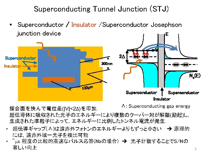
Superconducting Tunnel Junction (STJ) • Superconductor / Insulator /Superconductor Josephson junction device E 2 Superconductor 300 nm Insulator Ns(E) 100 m Superconductor Insulator Δ: Superconducting gap energy • 超伝導ギャップ(Δ)は遠赤外フォトンのエネルギーよりもずっと小さい 原理的 には,遠赤外域一光子を検出可能 • ~ s 程度の比較的高速なパルス応答(Nbの場合) 光子計数することでS/Nの 著しい向上 2
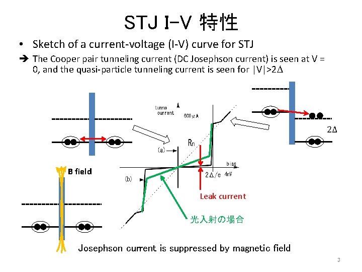
STJ I-V 特性 • Sketch of a current-voltage (I-V) curve for STJ The Cooper pair tunneling current (DC Josephson current) is seen at V = 0, and the quasi-particle tunneling current is seen for |V|>2 B field Leak current 光入射の場合 Josephson current is suppressed by magnetic field 3
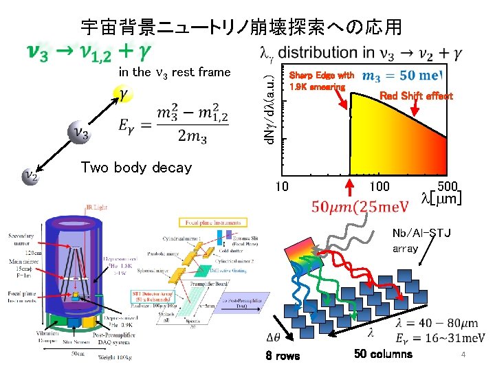
宇宙背景ニュートリノ崩壊探索への応用 in the 3 rest frame d. N /d (a. u. ) Sharp Edge with 1. 9 K smearing Red Shift effect Two body decay 10 100 500 [ m] Nb/Al-STJ array 8 rows 50 columns 4
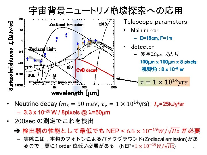
Surface brightness I [MJy/sr] 宇宙背景ニュートリノ崩壊探索への応用 Zodiacal Emission CMB Telescope parameters • Main mirror – D=15 cm, F=1 m • detector Zodiacal Light ISD DGL C B decay – 波長 0. 8 m あたり 100 m x 8 pixels 視野角 : 8 x 10 -8 sr SL Integrated flux from galaxy counts wavelength [ m] 5
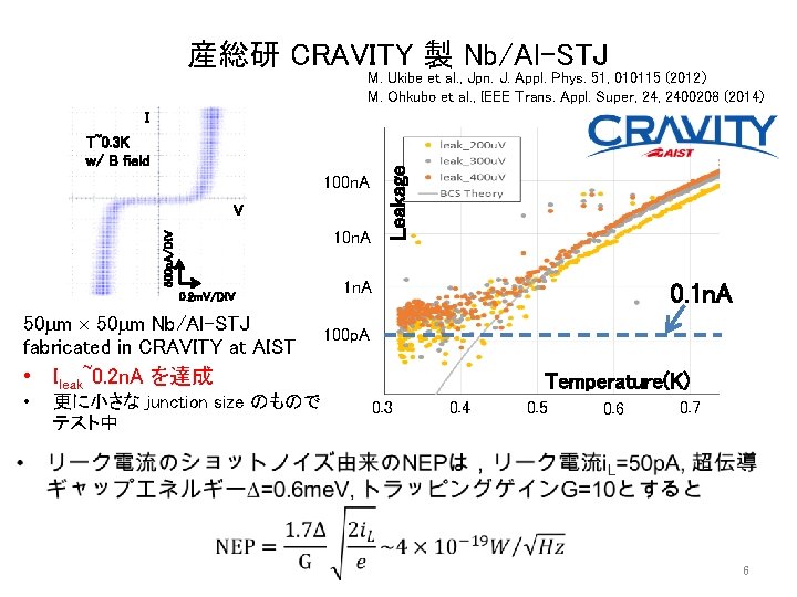
産総研 CRAVITY 製 Nb/Al-STJ M. Ukibe et al. , Jpn. J. Appl. Phys. 51, 010115 (2012) M. Ohkubo et al. , IEEE Trans. Appl. Super, 2400208 (2014) T~0. 3 K w/ B field 100 n. A V 500 p. A/DIV 10 n. A 0. 2 m. V/DIV 50 m Nb/Al-STJ fabricated in CRAVITY at AIST Leakage I 1 n. A 0. 1 n. A 100 p. A • Ileak~0. 2 n. A を達成 • 更に小さな junction size のもので テスト中 Temperature(K) 0. 3 0. 4 0. 5 0. 6 0. 7 6
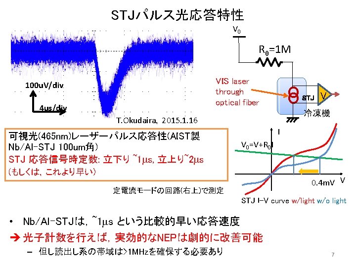
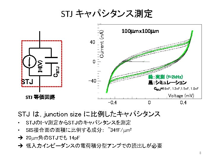
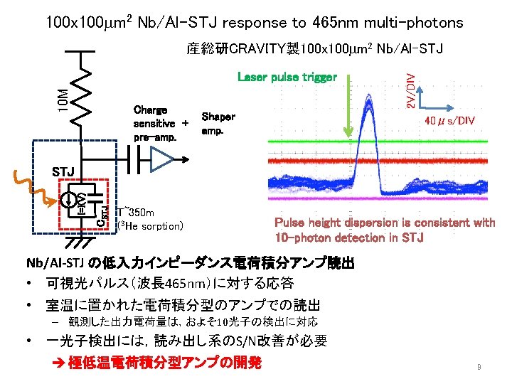
100 x 100 m 2 Nb/Al-STJ response to 465 nm multi-photons 10 M Laser pulse trigger Charge sensitive + pre-amp. Shaper amp. 2 V/DIV 産総研CRAVITY製 100 x 100 m 2 Nb/Al-STJ 40μs/DIV CSTJ I=I(V) STJ T~350 m (3 He sorption) Pulse height dispersion is consistent with 10 -photon detection in STJ Nb/Al-STJ の低入力インピーダンス電荷積分アンプ読出 • 可視光パルス(波長 465 nm)に対する応答 • 室温に置かれた電荷積分型のアンプでの読出 – 観測した出力電荷量は,およそ 10光子の検出に対応 • 一光子検出には,読み出し系のS/N改善が必要 極低温電荷積分型アンプの開発 9
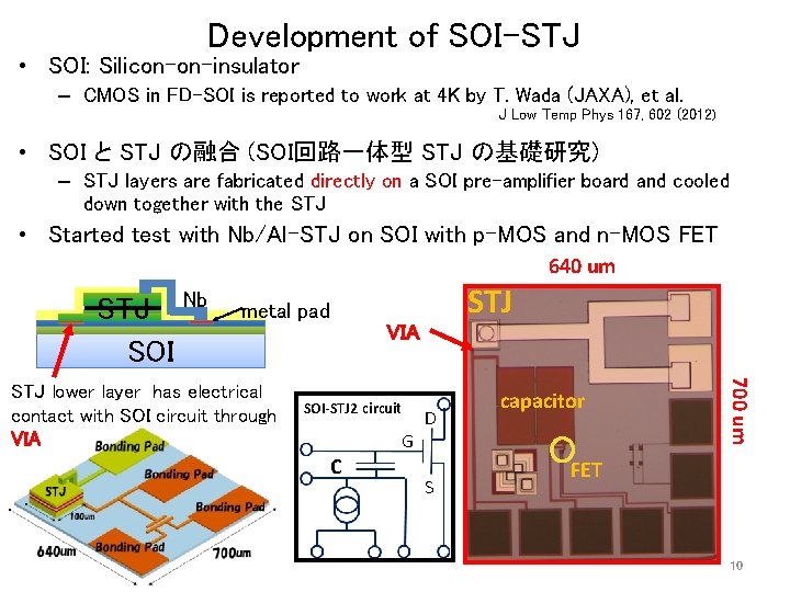
Development of SOI-STJ • SOI: Silicon-on-insulator – CMOS in FD-SOI is reported to work at 4 K by T. Wada (JAXA), et al. J Low Temp Phys 167, 602 (2012) • SOI と STJ の融合 (SOI回路一体型 STJ の基礎研究) – STJ layers are fabricated directly on a SOI pre-amplifier board and cooled down together with the STJ • Started test with Nb/Al-STJ on SOI with p-MOS and n-MOS FET 640 um STJ Nb SOI STJ metal pad SOI-STJ 2 circuit C G D S capacitor 700 um STJ lower layer has electrical contact with SOI circuit through VIA FET 10
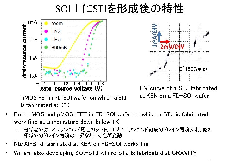
1 m. A/DIV drain-source current SOI上にSTJを形成後の特性 1 A 2 m. V/DIV 1 n. A B~150 Gauss 1 p. A -0. 2 0. 4 0. 6 0. 8 gate-source voltage (V) n. MOS-FET in FD-SOI wafer on which a STJ is fabricated at KEK I-V curve of a STJ fabricated at KEK on a FD-SOI wafer • Both n. MOS and p. MOS-FET in FD-SOI wafer on which a STJ is fabricated work fine at temperature down below 1 K – 極低温では,スレッショルド電圧のシフト,サブスレッショルド領域のドレイン電流抑制,飽和 領域でのドレイン電流の上昇など,特性が変動 • Nb/Al-STJ fabricated at KEK on FD-SOI works fine • We are also developing SOI-STJ where STJ is fabricated at CRAVITY 11

Backup 14
Neutrino • 15
Density (cm-3) C B (=neutrino decoupling) ~1 s after the big bang The universe is filled with neutrinos. However, they have not been detected yet! 16
Motivation of -decay search in C B • SM: SU(2)Lx U(1)Y PRL 38, (1977)1252, PRD 17(1978)1395 LRS: SU(2)LxSU(2)RxU(1)B-L 1026 enhancement to SM 17
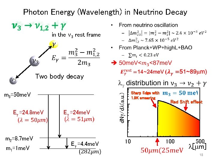
Photon Energy (Wavelength) in Neutrino Decay in the 3 rest frame m 3=50 me. V E =24. 8 me. V m 2=8. 7 me. V m 1=1 me. V E =24 me. V E =4. 4 me. V d. N /d (a. u. ) Two body decay Sharp Edge with 1. 9 K smearing 10 Red Shift effect 100 500 [ m] 18
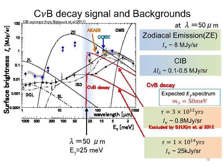
Surface brightness I [MJy/sr] CIB summary from Matsuura et al. (2011) ZE AKARI COBE CMB ZL ISD DGL at λ= 50μm C B decay SL wavelength [ m] E [me. V] λ= 50 μm E =25 me. V Excluded by S. H. Kim et. al 2012 19
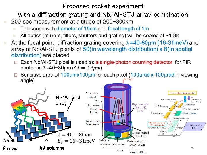
Proposed rocket experiment with a diffraction grating and Nb/Al-STJ array combination Nb/Al-STJ array 8 rows 50 columns 20
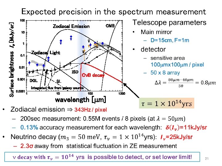
Surface brightness I [MJy/sr] Expected precision in the spectrum measurement Zodiacal Emission CMB • Zodiacal Light ISD DGL C B decay SL Integrated flux from galaxy counts wavelength [ m] 21
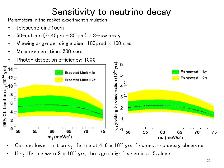
Sensitivity to neutrino decay Parameters in the rocket experiment simulation • • • telescope dia. : 15 cm 50 -column ( : 40 m – 80 m) 8 -row array Viewing angle per single pixel: 100 rad Measurement time: 200 sec. Photon detection efficiency: 100% • • Can set lower limit on 3 lifetime at 4 -6 1014 yrs if no neutrino decay observed If 3 lifetime were 2 1014 yrs, the signal significance is at 5 level 22
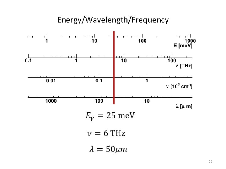
Energy/Wavelength/Frequency 23
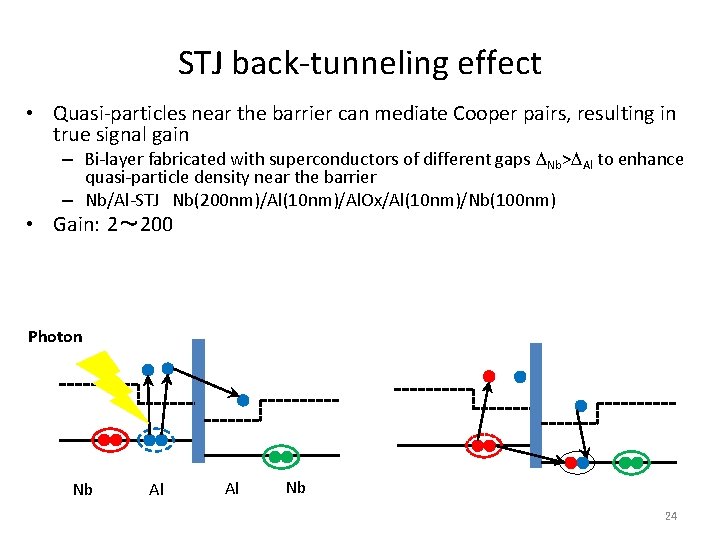
STJ back-tunneling effect • Quasi-particles near the barrier can mediate Cooper pairs, resulting in true signal gain – Bi-layer fabricated with superconductors of different gaps Nb> Al to enhance quasi-particle density near the barrier – Nb/Al-STJ Nb(200 nm)/Al(10 nm)/Al. Ox/Al(10 nm)/Nb(100 nm) • Gain: 2~ 200 Photon Nb Al Al Nb 24
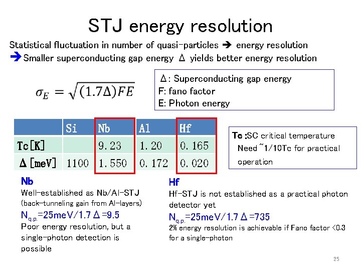
STJ energy resolution Statistical fluctuation in number of quasi-particles energy resolution Smaller superconducting gap energy Δ yields better energy resolution Δ: Superconducting gap energy F: fano factor E: Photon energy Si Tc[K] Nb Al Hf 9. 23 1. 20 0. 165 0. 172 0. 020 Δ[me. V] 1100 1. 550 Tc : SC critical temperature Need ~1/10 Tc for practical operation Nb Hf Well-established as Nb/Al-STJ Hf-STJ is not established as a practical photon detector yet (back-tunneling gain from Al-layers) Nq. p. =25 me. V/1. 7Δ=9. 5 Poor energy resolution, but a single-photon detection is possible Nq. p. =25 me. V/1. 7Δ=735 2% energy resolution is achievable if Fano factor <0. 3 for a single-photon 25
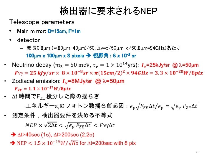
検出器に要求されるNEP Telescope parameters • Main mirror: D=15 cm, F=1 m • detector – 波長 0. 8 m (=(80 m-40 m)/50, =c/50 m-c/50. 8 m=94 GHz)あたり 100 m x 8 pixels 視野角 : 8 x 10 -8 sr 26
- Slides: 26