
Snovanje vgrajenih sistemov z veziji FPGA Anton Biasizzo

Snovanje vgrajenih sistemov z veziji FPGA Anton Biasizzo Odsek za računalniške sisteme
Outline • • Introduction FPGA structure Embedded system on FPGA design platform Embedded system design on FPGA Embedded software design FPGA Embedded design with Programmable Logic Software debugging

Introduction • Field Programmable Gate Array • Integrated circuit that can be programmed after manufacturing (at field) • First FPGA in 1984 (Altera EP 300) • Initially primarily used in telecommunication and networking • Spread to consumer, automotive, and industrial applications • Used for acceleration (Bing search engine), in data centers (Amazon AWS)
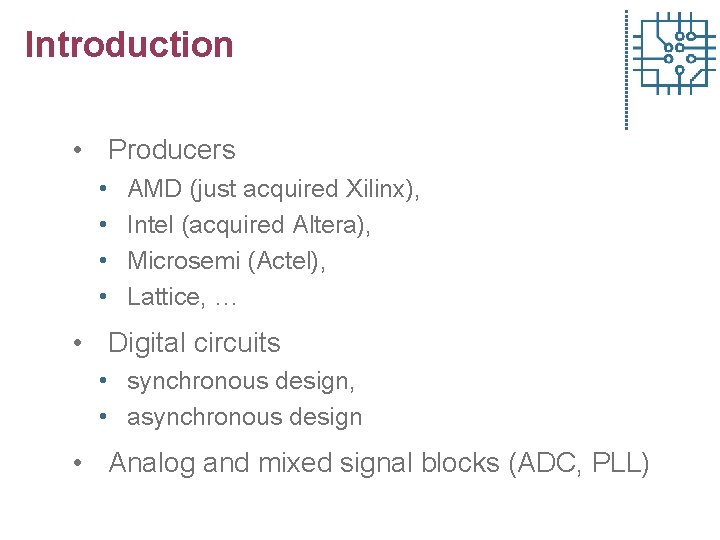
Introduction • Producers • • AMD (just acquired Xilinx), Intel (acquired Altera), Microsemi (Actel), Lattice, … • Digital circuits • synchronous design, • asynchronous design • Analog and mixed signal blocks (ADC, PLL)
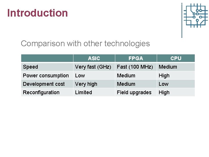
Introduction Comparison with other technologies ASIC FPGA CPU Speed Very fast (GHz) Fast (100 MHz) Medium Power consumption Low Medium High Development cost Very high Medium Low Reconfiguration Limited Field upgrades High
Outline • • Introduction FPGA structure FPGA design platform Design simulation Synthesis and implementation Design analysis Design debugging High level synthesis
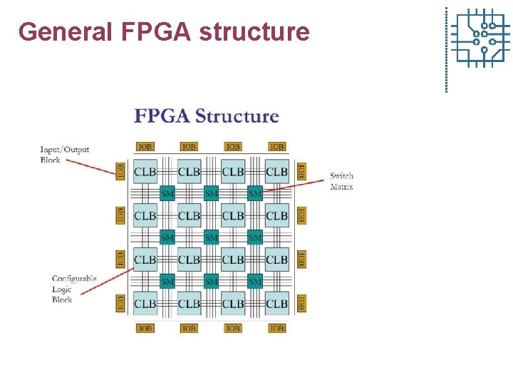
General FPGA structure
Configuration memory • 2 D array of frames • Technology • Volatile memory: SRAM (Xilinx, Intel) • Non-volatile memory • Flash (Microsemi, Lattice) • EPROM, EEPROM (obsolete) • fuses • Vulnerable to radiation induced faults (SEU) • Error correction techniques
Outline • • Introduction FPGA structure Embedded system on FPGA design platform Embedded system design on FPGA Embedded software design FPGA Embedded design with Programmable Logic Software debugging
FPGA hardware resources • • Logic blocks (CLB or slice) IOB Memory DSP blocks (computational blocks) Switching matrix Clock sources Special blocks (e. g. ICAP) Analog or mixed signal blocks
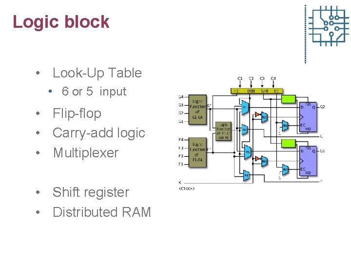
Logic block • Look-Up Table • 6 or 5 input • Flip-flop • Carry-add logic • Multiplexer • Shift register • Distributed RAM
Input / Output Block • Interface to chip pins • Support voltage levels for different semiconductor technologies • TTL, CMOS, … • Different speed: • General purpose interface (majority of IO pins) • High performance interface (DDR, PCI, Ethernet) • Latching flip-flops • Buffers on the IO pins
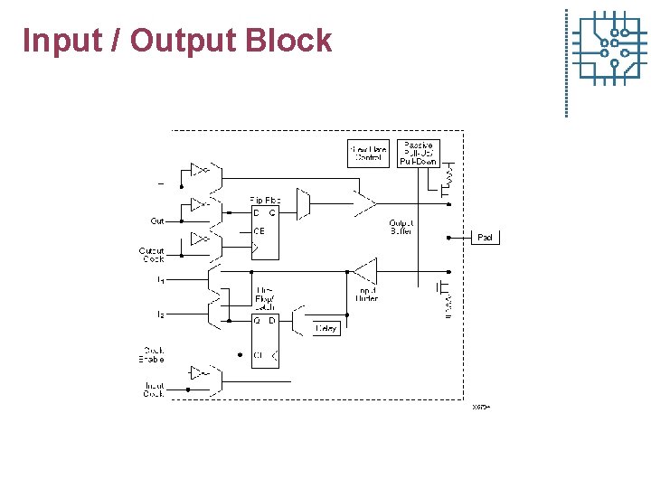
Input / Output Block
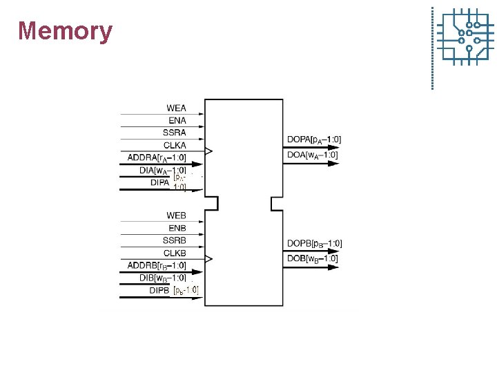
Memory • • • Distributed memory consumes logic blocks Block RAM (memory cores) Synchronous memory 2 x 18 kb or 36 kb RAM blocks Single/Dual port RAM Used for • Buffers • FIFOs • Integrated error correction
Memory
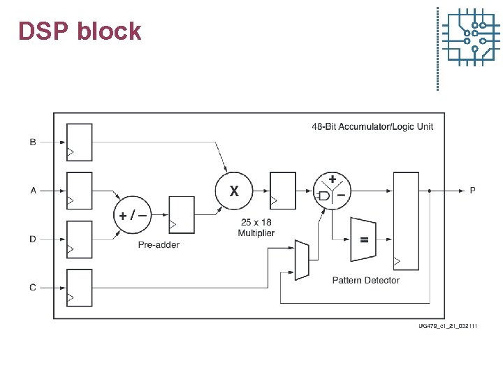
DSP block • • 25 x 18 multiplier 48 bit adder 48 bit logic operators Pipeline registers Pattern detectors SIMD operations Pre-adder
DSP block
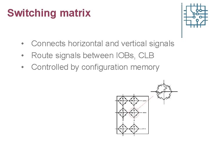
Switching matrix • Connects horizontal and vertical signals • Route signals between IOBs, CLB • Controlled by configuration memory
Clock sources • Global clock buffer • High fan-out clock distribution buffer • Low-skew clock distribution • Clock regions • Clock management tile (CMT) • One Mixed-Mode Clock Manager (MMCM) and one Phase-Locked Loop (PLL) per clock • Frequency synthesis, clock de-skew, and jitter filter
Special blocks • ICAP interface • Dynamic partial reconfiguration • SEM controller • Soft Error Mitigation controller • • Frame ECC interface Status interface Error Injection interface Monitor interface, …
Analog or mixed signal blocks • XADC block introduced in latest Xilinx 7 -series and Zynq family • Dual 12 -bit 1 Msps ADC • 17 analog inputs • 1 V input range • 16 bit resolution • Built in digital gain and offset calibration
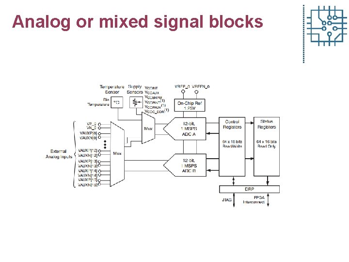
Analog or mixed signal blocks
Xilinx FPGA device families • XC series (from 1984) • Spartan series • Virtex – high performance family With 7 -series Xilinx introduced new families: • Artix – low power and cost • Kintex – best price/performance ratio • Zynq – So. C with hard ARM processor core
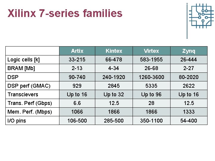
Xilinx 7 -series families Artix Kintex Virtex Zynq 33 -215 66 -478 583 -1955 26 -444 2 -13 4 -34 26 -68 2 -27 90 -740 240 -1920 1260 -3600 80 -2020 929 2845 5335 2622 Up to 16 Up to 32 Up to 96 Up to 16 Trans. Perf (Gbps) 6. 6 12. 5 28 12. 5 Mem. Perf. (Mbps) 1066 1866 1333 106 -500 285 -500 350 -1100 54 -400 Logic cells [k] BRAM [Mb] DSP perf (GMAC) Transcievers I/O pins
Outline • • Introduction FPGA structure Embedded system on FPGA design platform Embedded system design on FPGA Embedded software design FPGA Embedded design with Programmable Logic Software debugging
System-on-Chip • Complete system implemented in an ASIC • System-on-Chip (So. C) can include: • Processor, • Memory (RAM and storage), • Other digital devices (timers, interfaces, . . . ), • Radio frequency components, • Mixed signal devices (ADC, DAC, . . . )
System-on-Chip on FPGA • All-programmable System-on-Chip (APSo. C) • Hardware devices can be modified • FPGA implementations • Soft processor: micro. Blaze, Nios, Leon, or 1200, . . . • Hard processor: Power. PC, ARM • Dedicated IP cores • On field upgrades
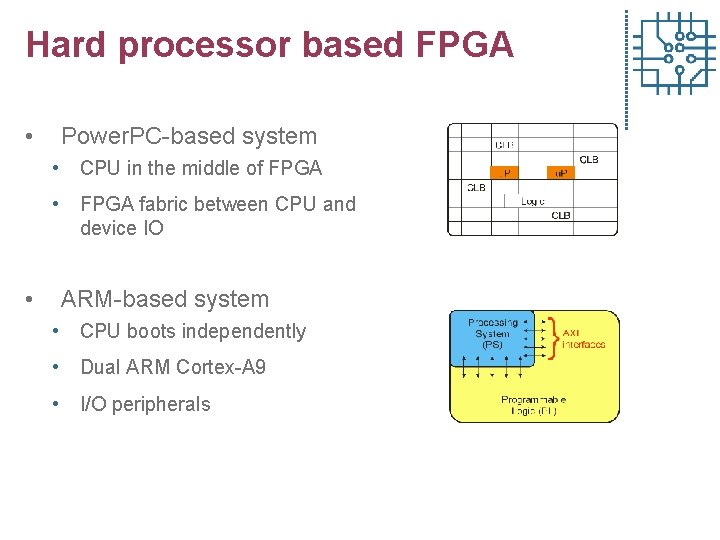
Hard processor based FPGA • Power. PC-based system • CPU in the middle of FPGA • FPGA fabric between CPU and device IO • ARM-based system • CPU boots independently • Dual ARM Cortex-A 9 • I/O peripherals
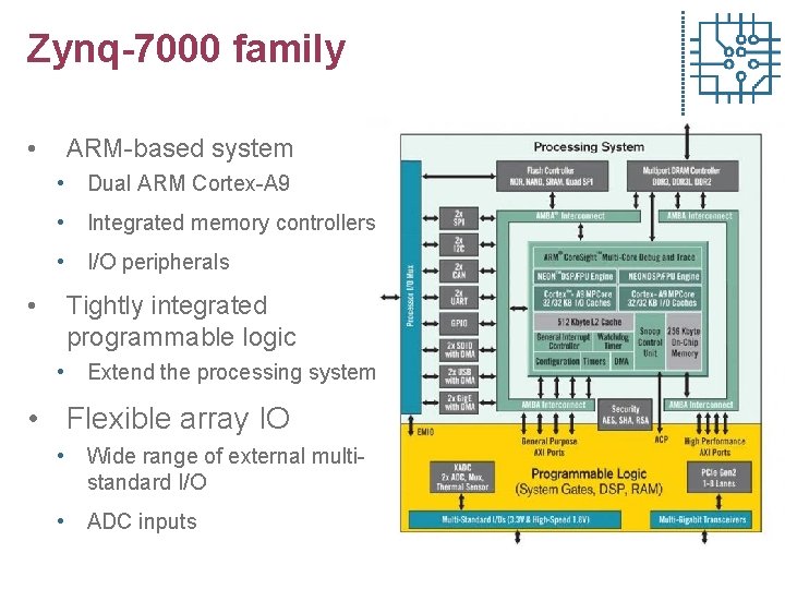
Zynq-7000 family • ARM-based system • Dual ARM Cortex-A 9 • Integrated memory controllers • I/O peripherals • Tightly integrated programmable logic • Extend the processing system • Flexible array IO • Wide range of external multistandard I/O • ADC inputs
Outline • • Introduction FPGA structure Embedded system on FPGA design platform Embedded system design on FPGA Embedded software design FPGA Embedded design with Programmable Logic Software debugging
Xilinx FPGA design flow Xilinx EDA Environments: • Xilinx ISE: • Xilinx stopped its support (latest version from 2014) • Supports older families – up to 7 -series • Xilinx Vivado • Supports Xilinx 7 -series and newer • Xilinx Vivado XLS • High-Level Synthesis • Xilinx SDAccel
Xilinx FPGA design flow • Tools support MS Windows and Linux OS • Xilinx ISE/Vivado functionality: • • Design Integrate existing IP cores into design Visualize and analyze design Simulate design Generate (build) configuration (place & route) Configure FPGA device Debug design
Xilinx FPGA design flow • Advanced features: • • Journaling Logging Batch processing Tcl command interface
Xilinx Vivado • Web. Pack: • • • Limited to smaller FPGA devices Synthesis HDL Simulation Logic analyzer High-level synthesis • Design edition: • All 7 -series devices and later devices • System edition: • System Generator for DSP

Xilinx Vivado • Hardware representation (Vivado HLx): • HDL languages: • VHDL language • Verilog • Not all code is synthesizable • Schematic capture is not supported • C / C++/ System. C (Vivado HLS) • Constraint specification • Timing constraints, clock definitions • I/O pin definitions
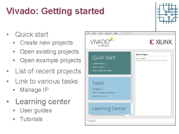
Vivado: Getting started • Quick start • Create new projects • Open existing projects • Open example projects • List of recent projects • Link to various tasks • Manage IP • Learning center • User guides • Tutorials
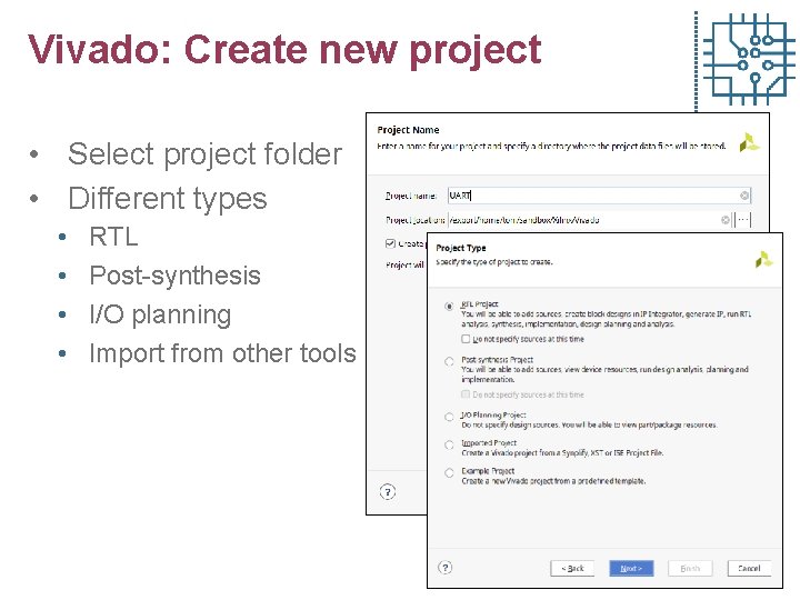
Vivado: Create new project • Select project folder • Different types • • RTL Post-synthesis I/O planning Import from other tools
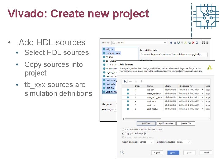
Vivado: Create new project • Add HDL sources • Select HDL sources • Copy sources into project • tb_xxx sources are simulation definitions
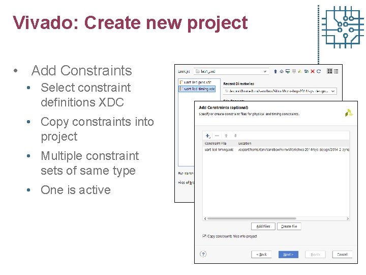
Vivado: Create new project • Add Constraints • Select constraint definitions XDC • Copy constraints into project • Multiple constraint sets of same type • One is active
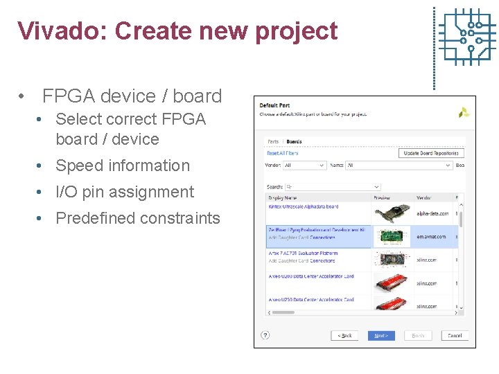
Vivado: Create new project • FPGA device / board • Select correct FPGA board / device • Speed information • I/O pin assignment • Predefined constraints
Vivado: Project manager • Manage source, customize IP, and view project details in the Project Summary window • Flow navigator • Source view: • Hierarchical display of sources • IP sources an library view • Access to constraint sources • Project summary • Report device utilization, timing, … • Consoles: tcl, messages, reports, …
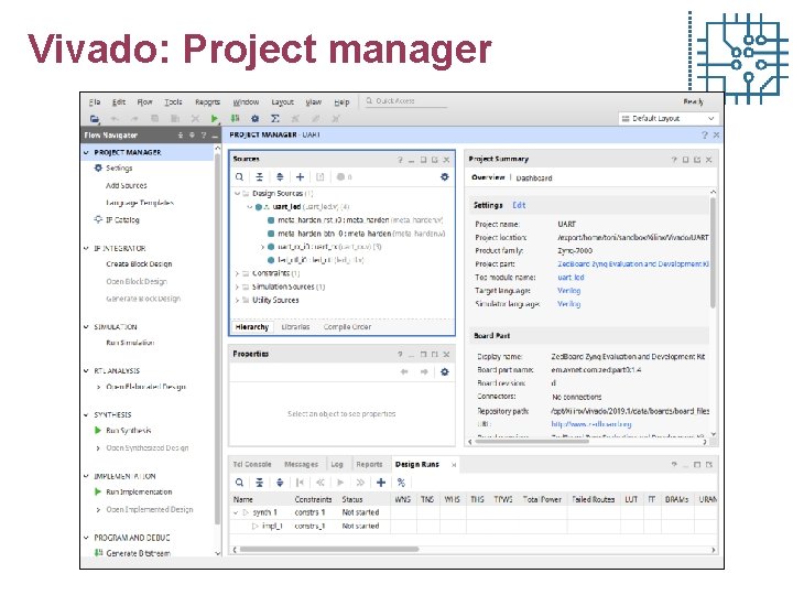
Vivado: Project manager
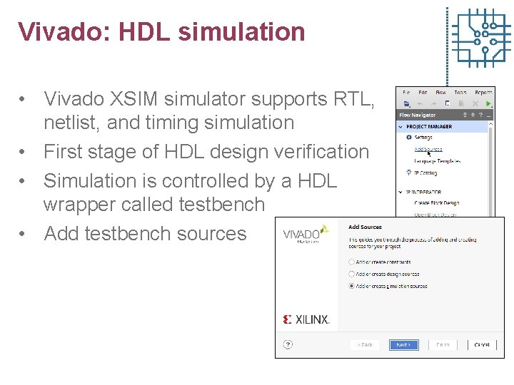
Vivado: HDL simulation • Vivado XSIM simulator supports RTL, netlist, and timing simulation • First stage of HDL design verification • Simulation is controlled by a HDL wrapper called testbench • Add testbench sources
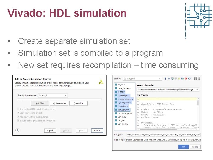
Vivado: HDL simulation • Create separate simulation set • Simulation set is compiled to a program • New set requires recompilation – time consuming
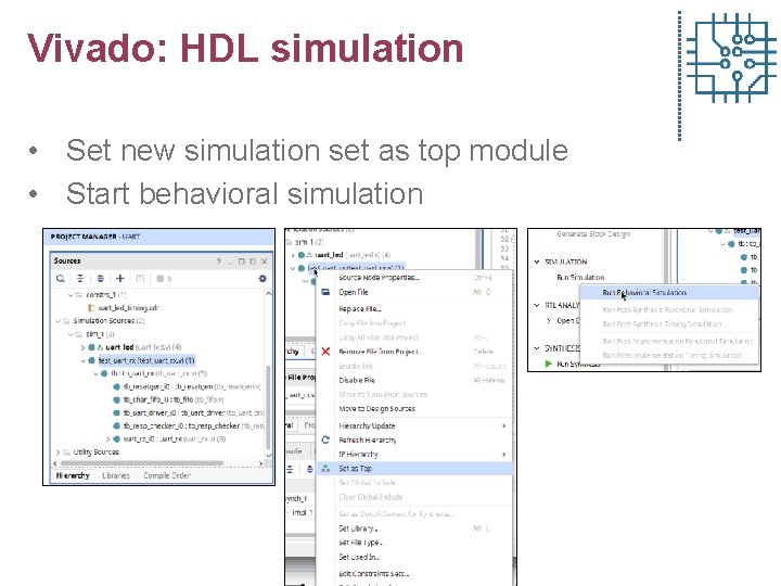
Vivado: HDL simulation • Set new simulation set as top module • Start behavioral simulation
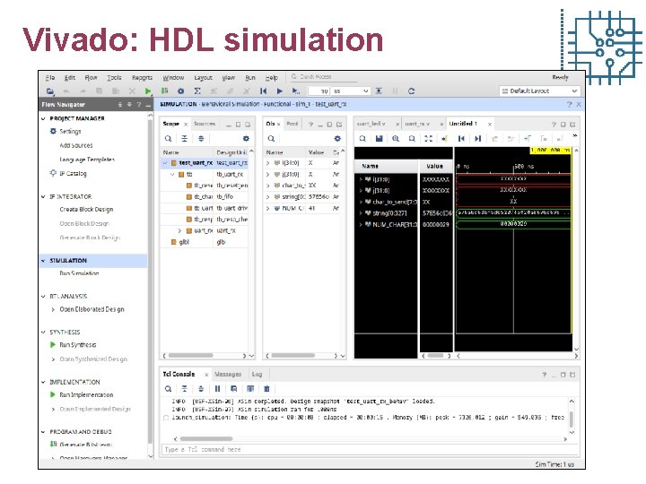
Vivado: HDL simulation
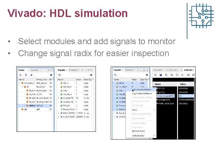
Vivado: HDL simulation • Select modules and add signals to monitor • Change signal radix for easier inspection
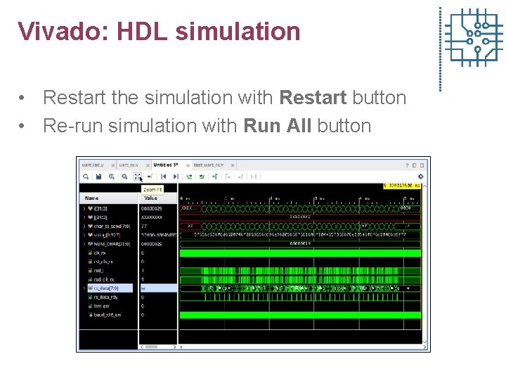
Vivado: HDL simulation • Restart the simulation with Restart button • Re-run simulation with Run All button
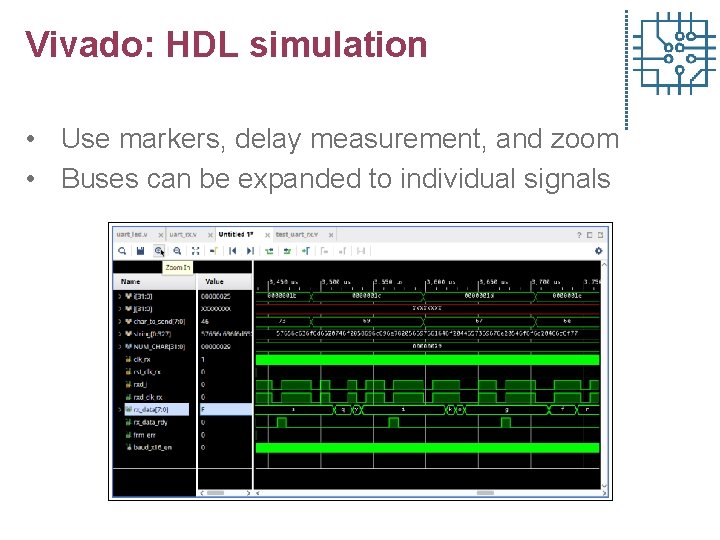
Vivado: HDL simulation • Use markers, delay measurement, and zoom • Buses can be expanded to individual signals
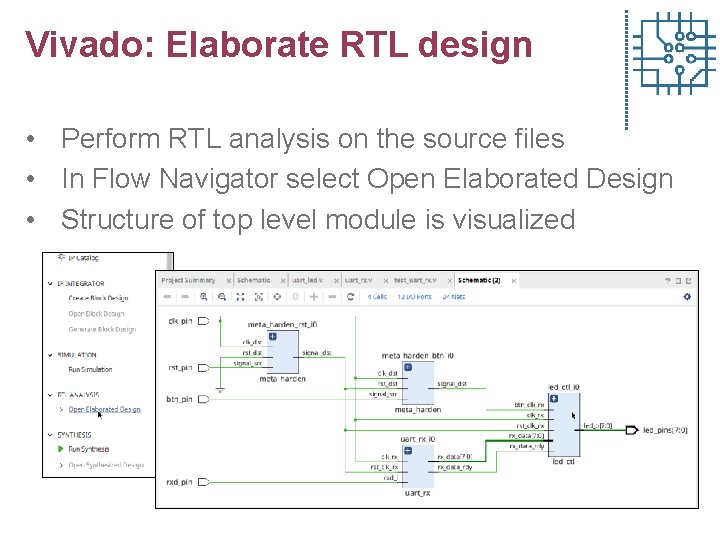
Vivado: Elaborate RTL design • Perform RTL analysis on the source files • In Flow Navigator select Open Elaborated Design • Structure of top level module is visualized
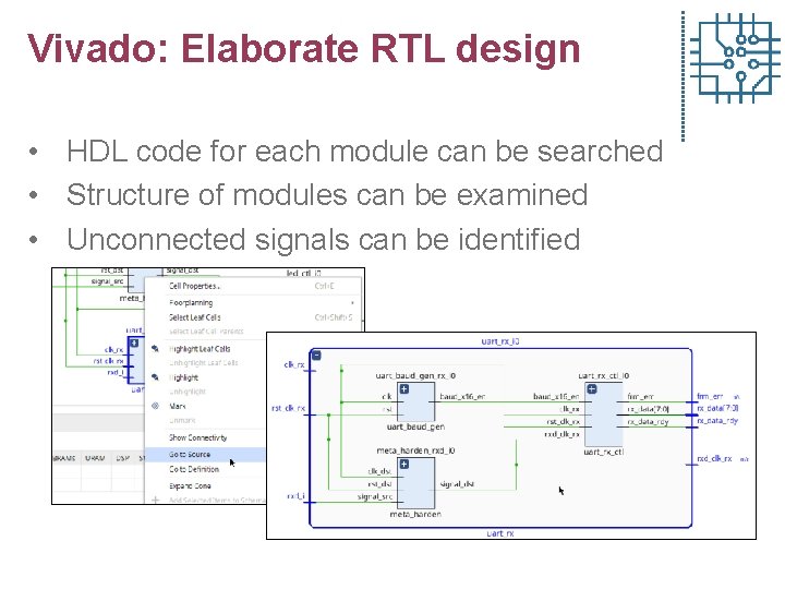
Vivado: Elaborate RTL design • HDL code for each module can be searched • Structure of modules can be examined • Unconnected signals can be identified
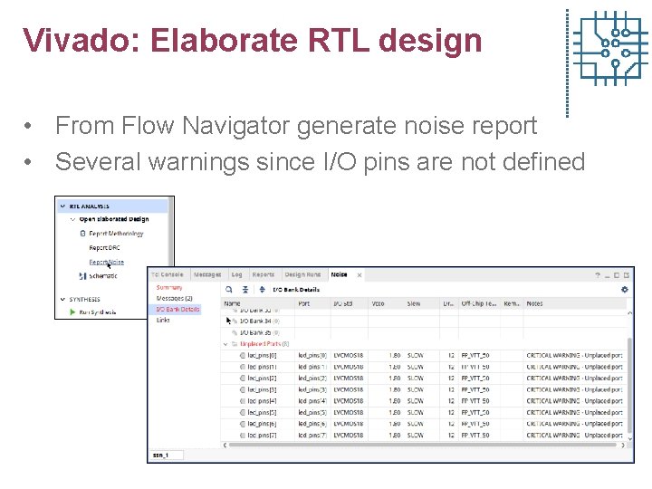
Vivado: Elaborate RTL design • From Flow Navigator generate noise report • Several warnings since I/O pins are not defined
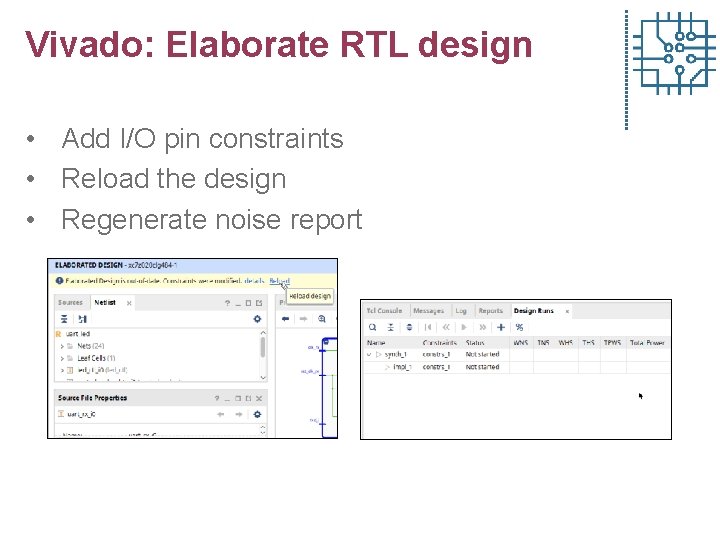
Vivado: Elaborate RTL design • Add I/O pin constraints • Reload the design • Regenerate noise report
Outline • • Introduction FPGA structure Embedded system on FPGA design platform Embedded system design on FPGA Embedded software design FPGA Embedded design with Programmable Logic Software debugging
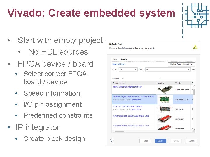
Vivado: Create embedded system • Start with empty project • No HDL sources • FPGA device / board • Select correct FPGA board / device • Speed information • I/O pin assignment • Predefined constraints • IP integrator • Create block design
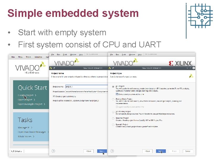
Simple embedded system • Start with empty system • First system consist of CPU and UART
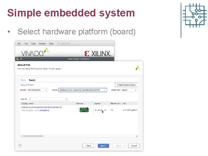
Simple embedded system • Select hardware platform (board)
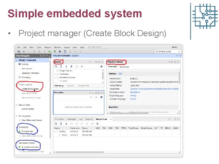
Simple embedded system • Project manager (Create Block Design)
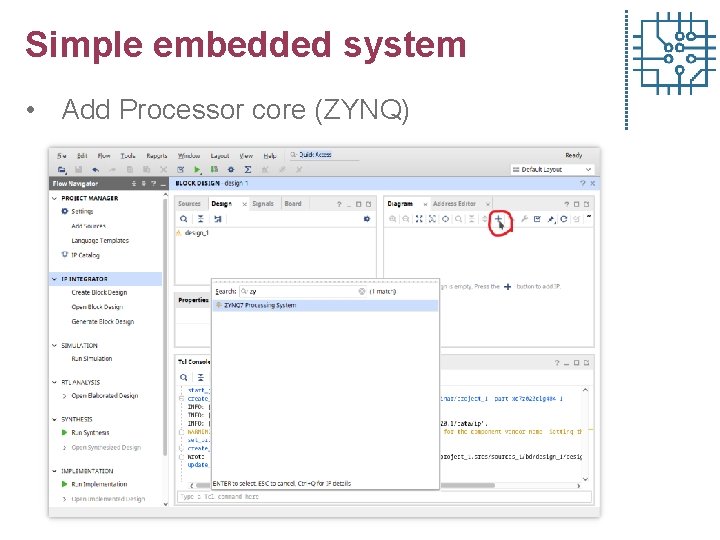
Simple embedded system • Add Processor core (ZYNQ)
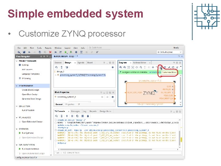
Simple embedded system • Customize ZYNQ processor
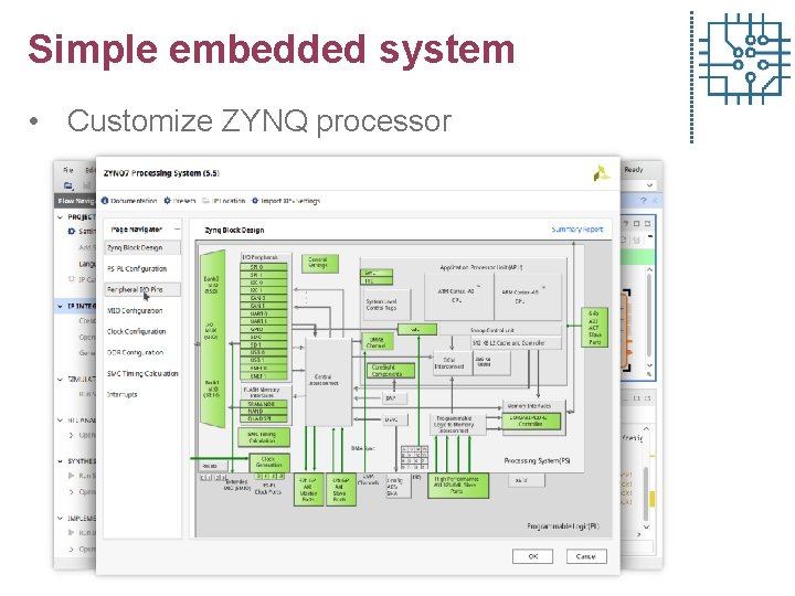
Simple embedded system • Customize ZYNQ processor
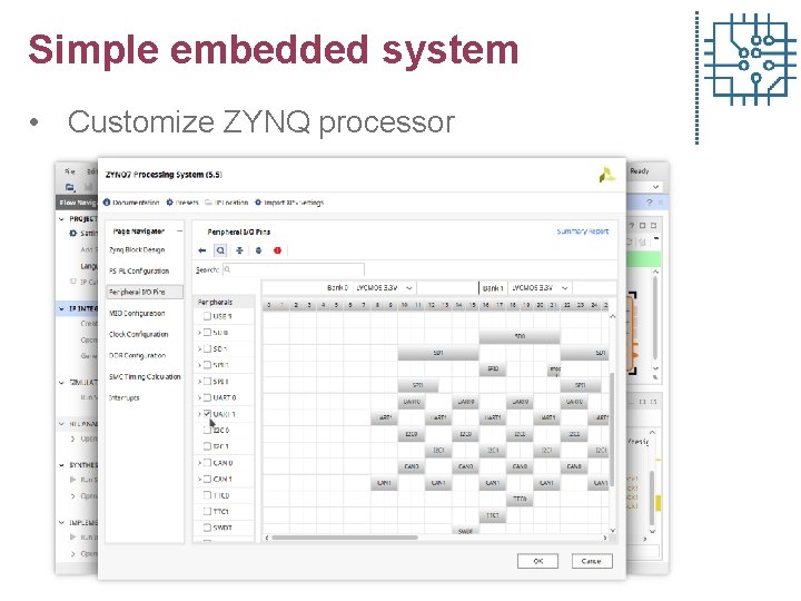
Simple embedded system • Customize ZYNQ processor
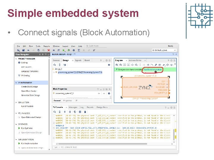
Simple embedded system • Connect signals (Block Automation)
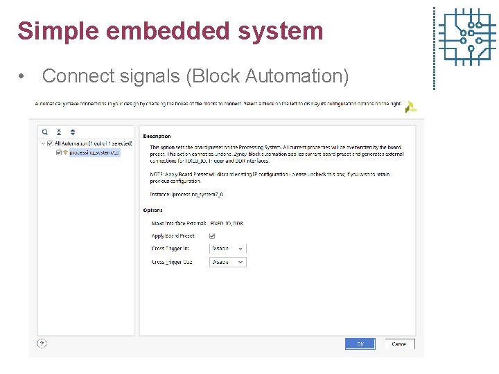
Simple embedded system • Connect signals (Block Automation)
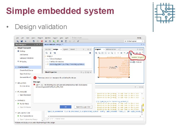
Simple embedded system • Design validation
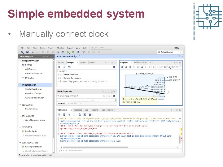
Simple embedded system • Manually connect clock
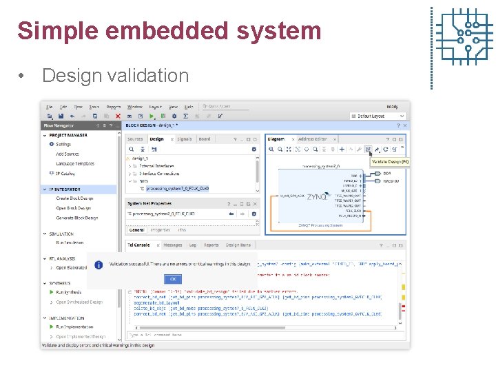
Simple embedded system • Design validation
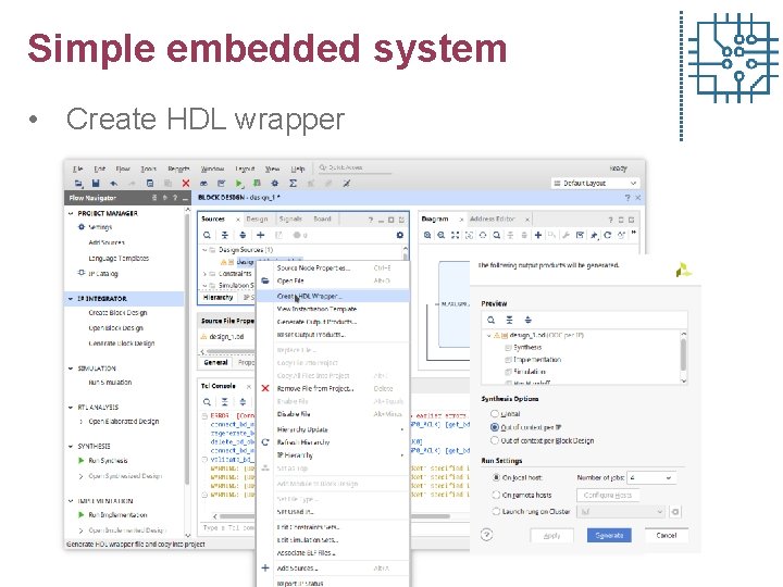
Simple embedded system • Create HDL wrapper
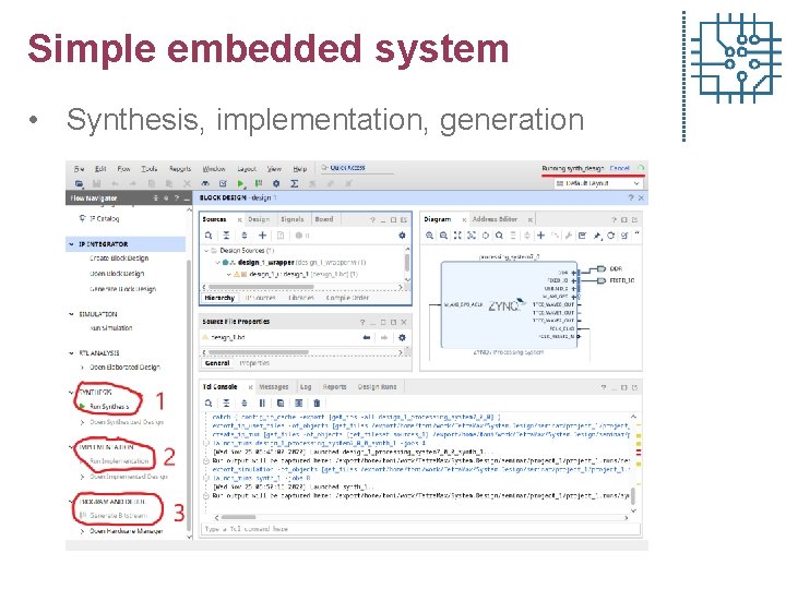
Simple embedded system • Synthesis, implementation, generation
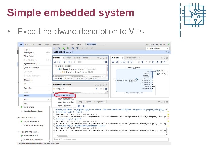
Simple embedded system • Export hardware description to Vitis
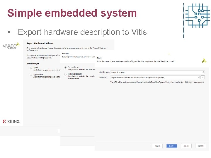
Simple embedded system • Export hardware description to Vitis
Outline • • Introduction FPGA structure Embedded system on FPGA design platform Embedded system design on FPGA Embedded software design FPGA Embedded design with Programmable Logic Software debugging
Vitis: Software Development Kit • • Unified software development environment Based on eclipse Requires hardware definition files (Vivado) Supports different types of applications: • Standalone • free. RTOS • Petalinux (proprietary) • Programming tools (over JTAG) • Debugging tools
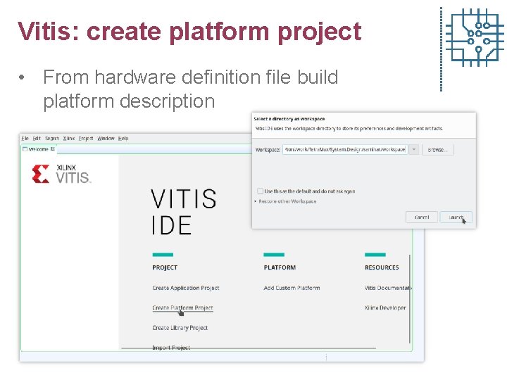
Vitis: create platform project • From hardware definition file build platform description
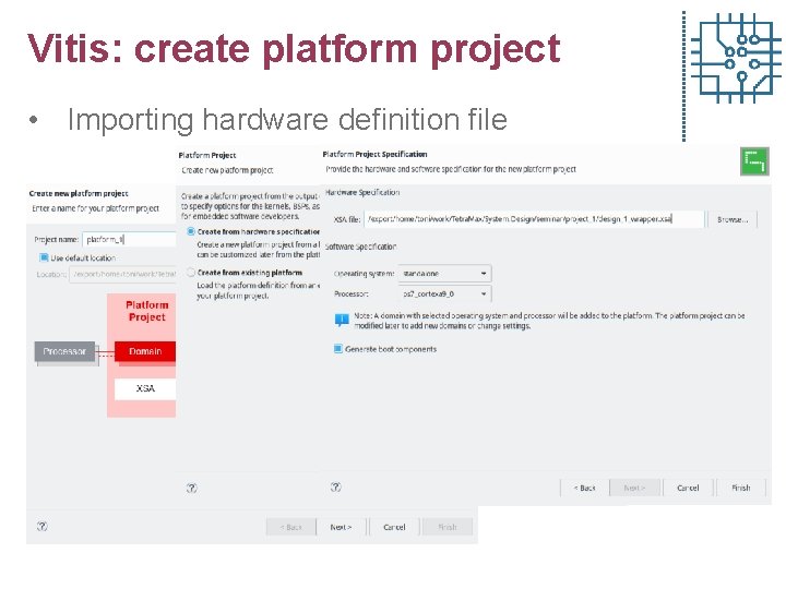
Vitis: create platform project • Importing hardware definition file
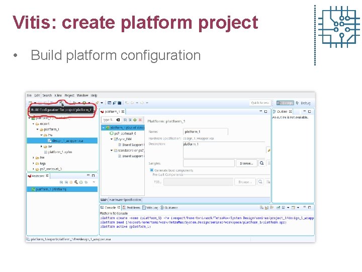
Vitis: create platform project • Build platform configuration
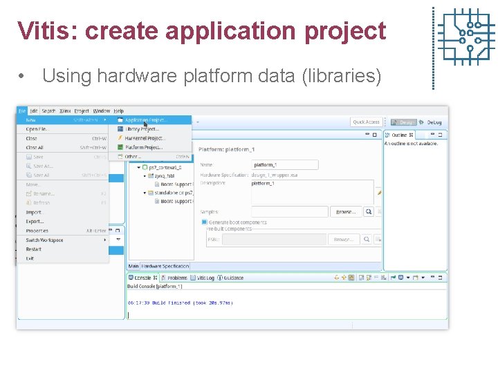
Vitis: create application project • Using hardware platform data (libraries)
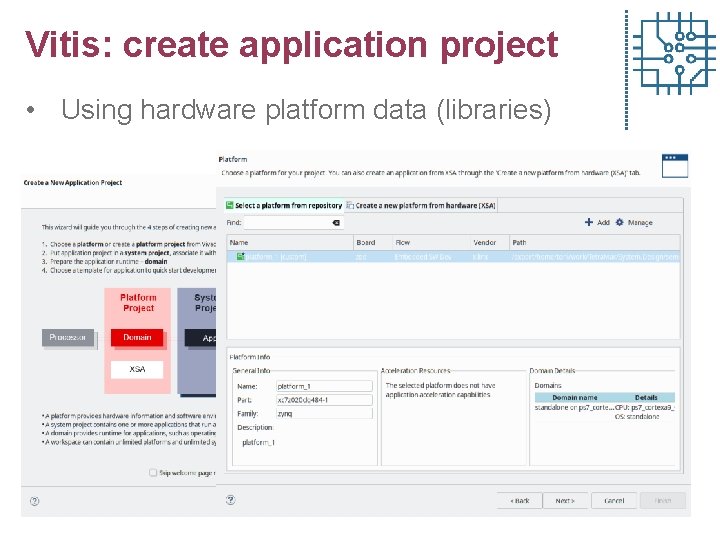
Vitis: create application project • Using hardware platform data (libraries)
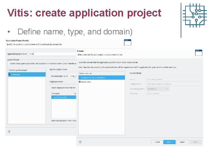
Vitis: create application project • Define name, type, and domain)
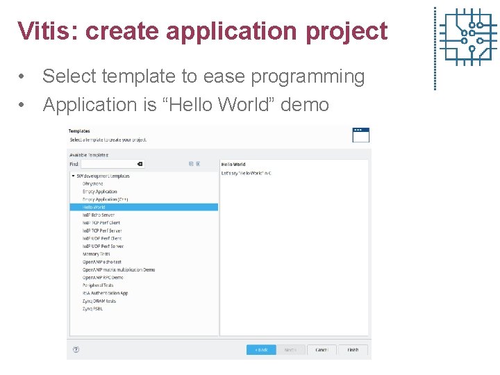
Vitis: create application project • Select template to ease programming • Application is “Hello World” demo
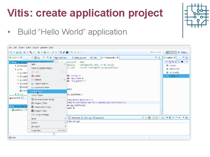
Vitis: create application project • Build “Hello World” application
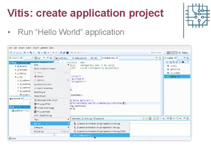
Vitis: create application project • Run “Hello World” application
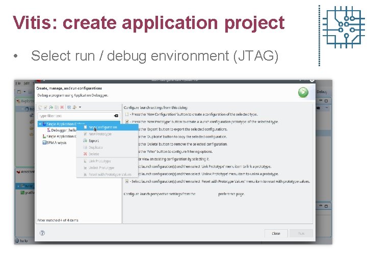
Vitis: create application project • Select run / debug environment (JTAG)
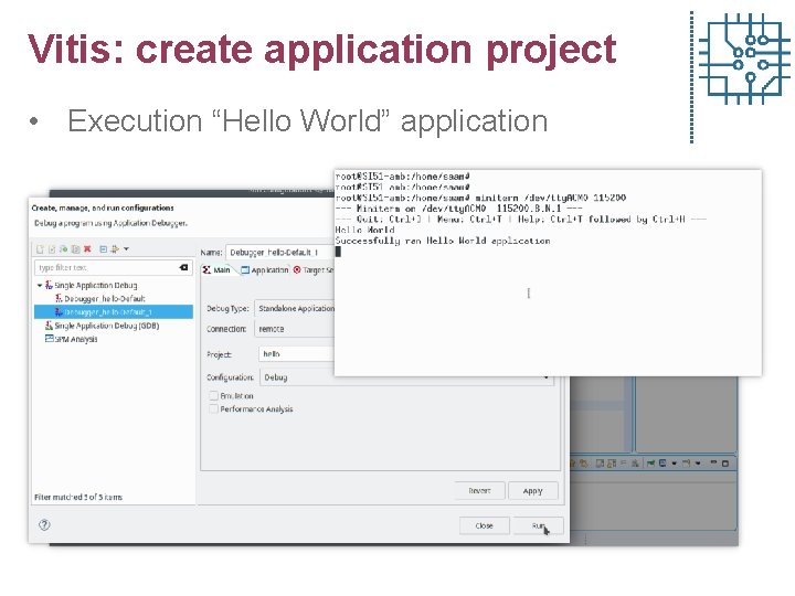
Vitis: create application project • Execution “Hello World” application
Outline • • Introduction FPGA structure Embedded system on FPGA design platform Embedded system design on FPGA Embedded software design FPGA Embedded design with PL part Software debugging
Embedded system with PL part • Start from previously build system • Use Zedboard prototyping board • Define two GPIO interfaces in PL • One attached to five push buttons • Other attached to eight slide buttons • Use available AXI-Lite cores
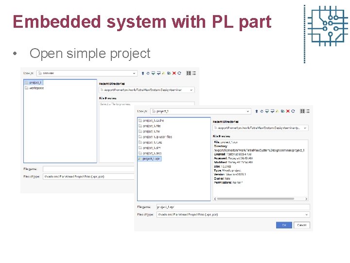
Embedded system with PL part • Open simple project
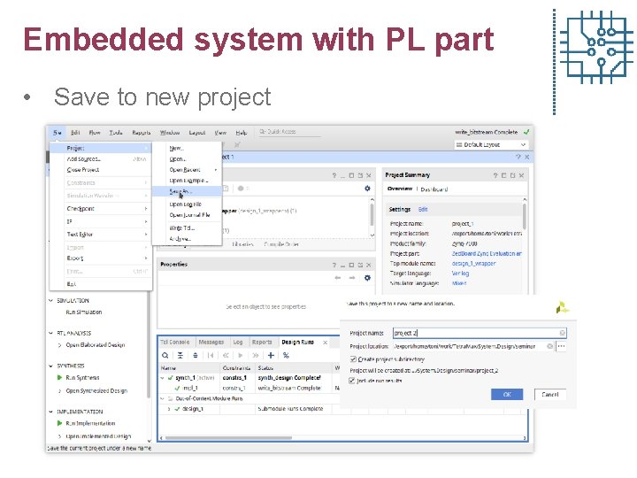
Embedded system with PL part • Save to new project
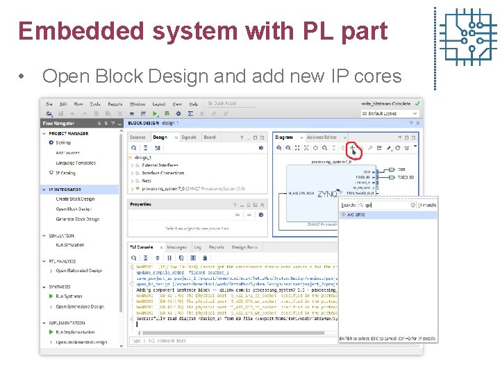
Embedded system with PL part • Open Block Design and add new IP cores
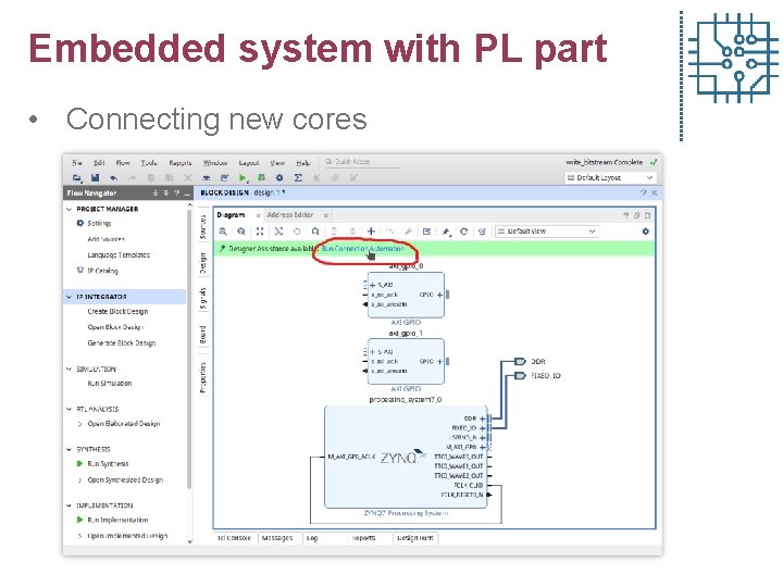
Embedded system with PL part • Connecting new cores
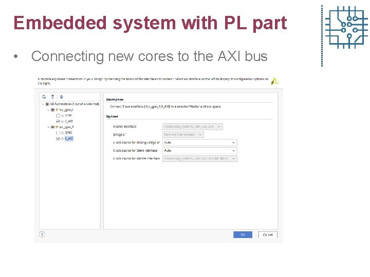
Embedded system with PL part • Connecting new cores to the AXI bus
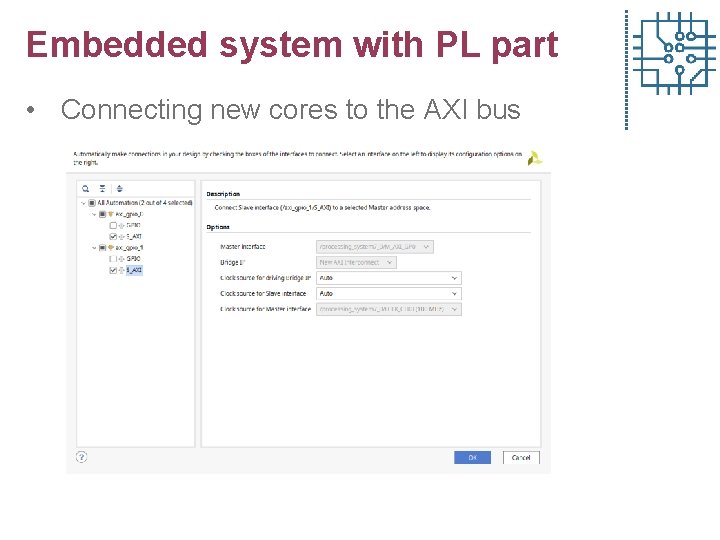
Embedded system with PL part • Connecting new cores to the AXI bus
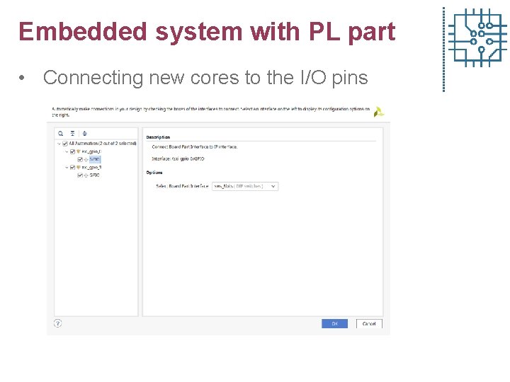
Embedded system with PL part • Connecting new cores to the I/O pins
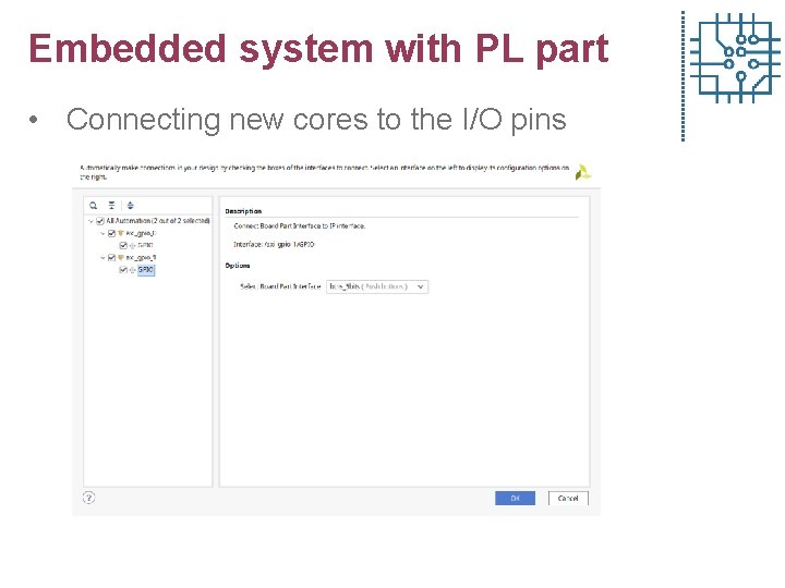
Embedded system with PL part • Connecting new cores to the I/O pins
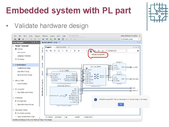
Embedded system with PL part • Validate hardware design
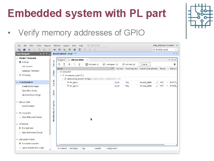
Embedded system with PL part • Verify memory addresses of GPIO
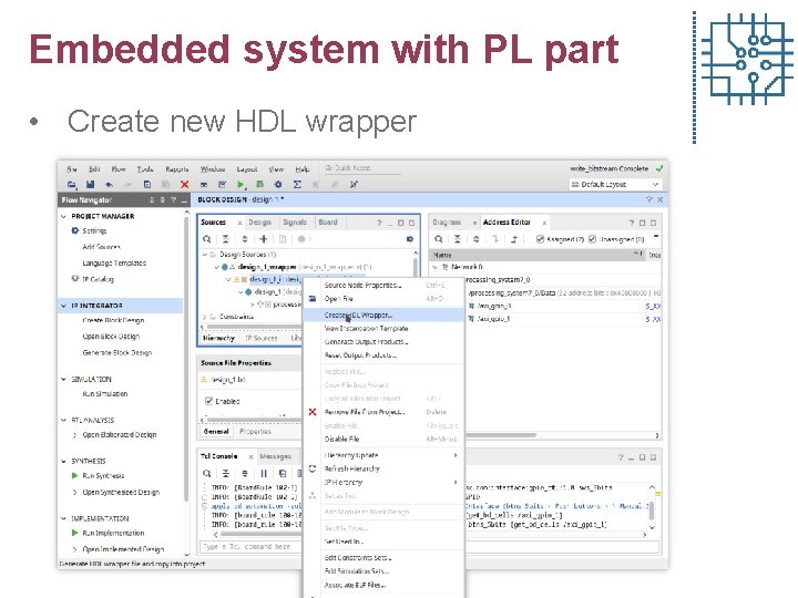
Embedded system with PL part • Create new HDL wrapper
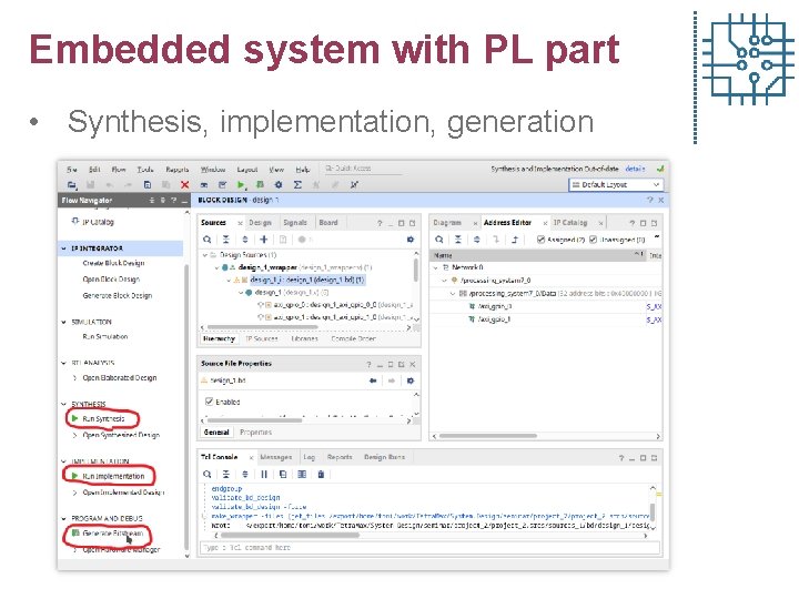
Embedded system with PL part • Synthesis, implementation, generation
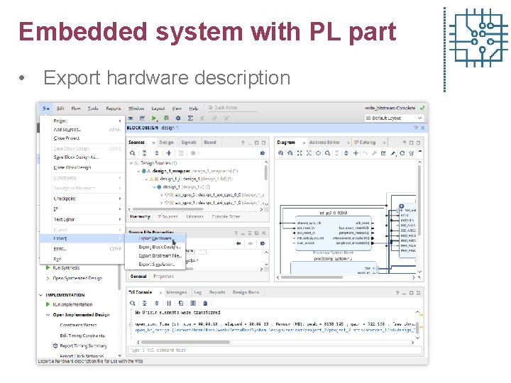
Embedded system with PL part • Export hardware description
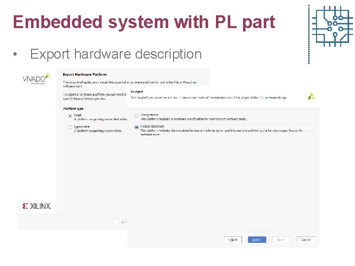
Embedded system with PL part • Export hardware description
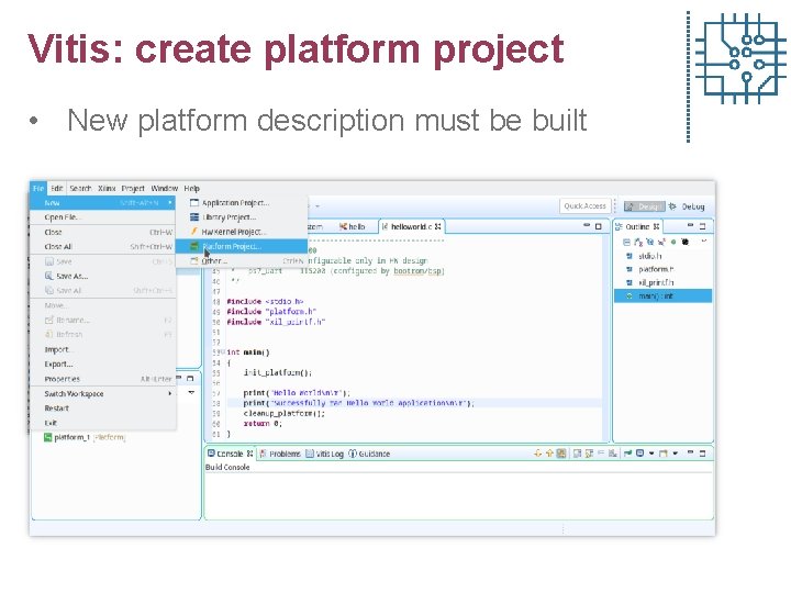
Vitis: create platform project • New platform description must be built
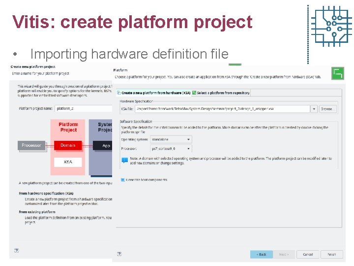
Vitis: create platform project • Importing hardware definition file
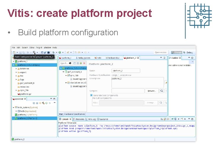
Vitis: create platform project • Build platform configuration
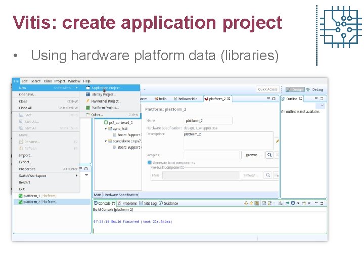
Vitis: create application project • Using hardware platform data (libraries)
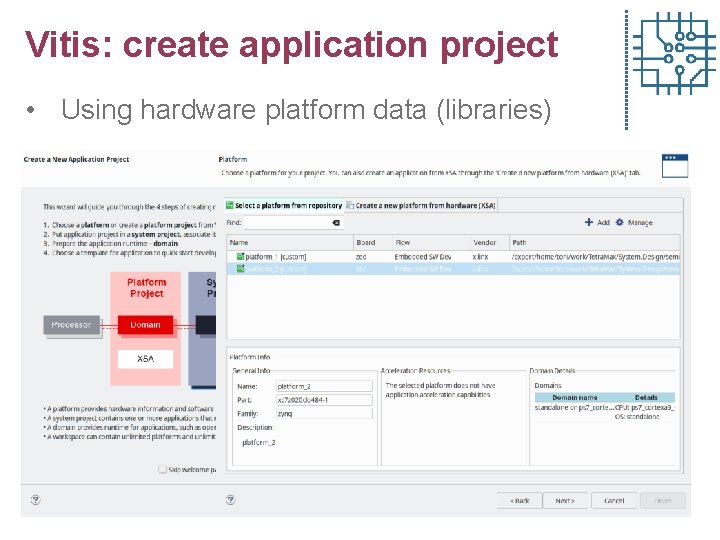
Vitis: create application project • Using hardware platform data (libraries)
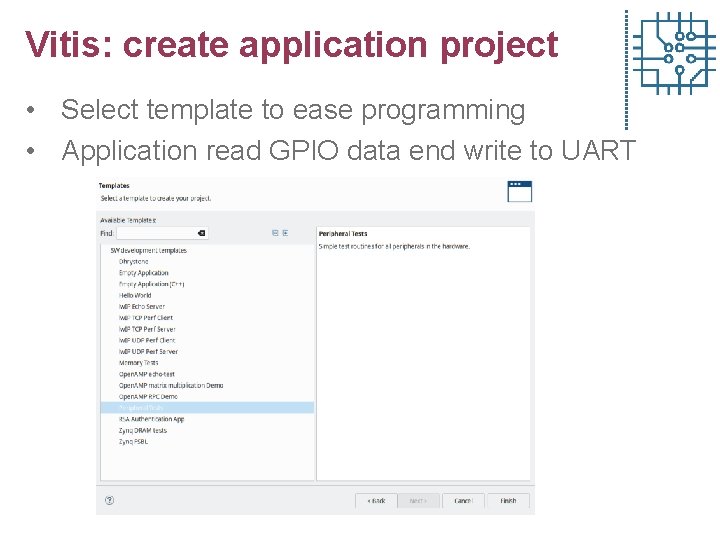
Vitis: create application project • Select template to ease programming • Application read GPIO data end write to UART
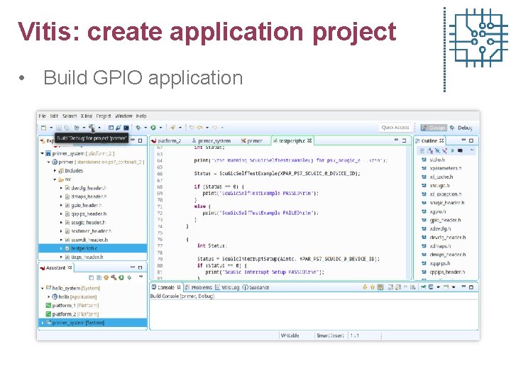
Vitis: create application project • Build GPIO application
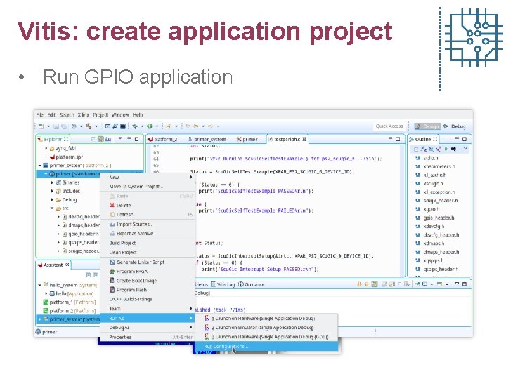
Vitis: create application project • Run GPIO application
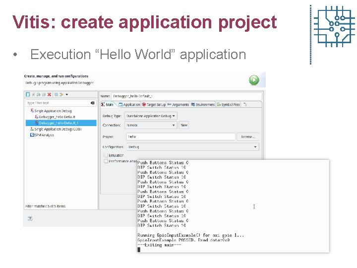
Vitis: create application project • Execution “Hello World” application
Outline • • Introduction FPGA structure Embedded system on FPGA design platform Embedded system design on FPGA Embedded software design FPGA Embedded design with Programmable Logic Software debugging
Vitis: Software debugging • Is part of the embedded toolkit • Is supported ove programming interface (Jtag) • Can be performed remotely • Applications must be build with enabled debugging • Debugging is enabled by default
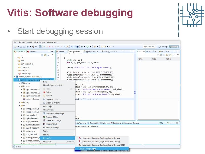
Vitis: Software debugging • Start debugging session

Vitis: Software debugging • Configuration is the same as in running
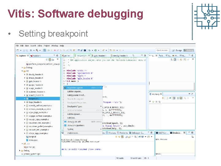
Vitis: Software debugging • Setting breakpoint
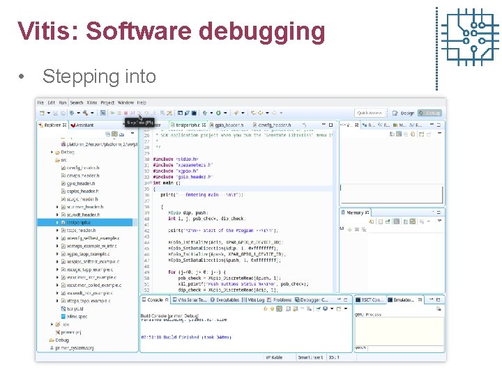
Vitis: Software debugging • Stepping into
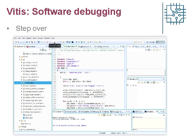
Vitis: Software debugging • Step over
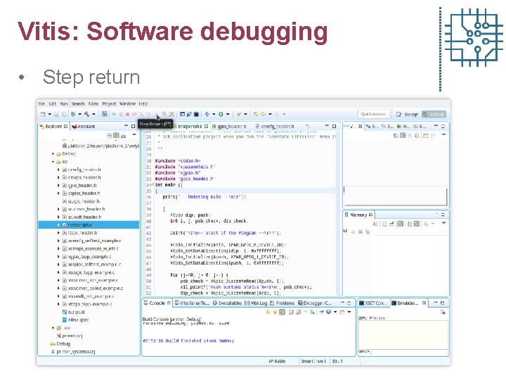
Vitis: Software debugging • Step return
- Slides: 117