SmallSignal Modeling Dr David W Graham West Virginia
- Slides: 27

Small-Signal Modeling Dr. David W. Graham West Virginia University Lane Department of Computer Science and Electrical Engineering © 2010 David W. Graham 1

Small-Signal Modeling • An approximation to the large-signal model around an operating point • Assumes perturbations in the bias conditions are small • Can use a linearized model for small changes 2

Small-Signal Modeling • Assumptions – Transistor is biased at some current level – Saturated operation (typically) – Only small potential changes at the terminals (G, S, D, B) • Consequences – DC bias levels (currents & voltages) can be ignored – Any voltage change at any terminal will modify the channel current 3

Different Small-Signal Models • Bulk-referred model • Source-referred model • T model 4

Bulk-Referred Small-Signal Model (Low Frequency) 5

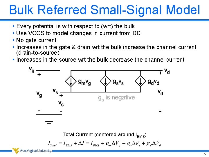
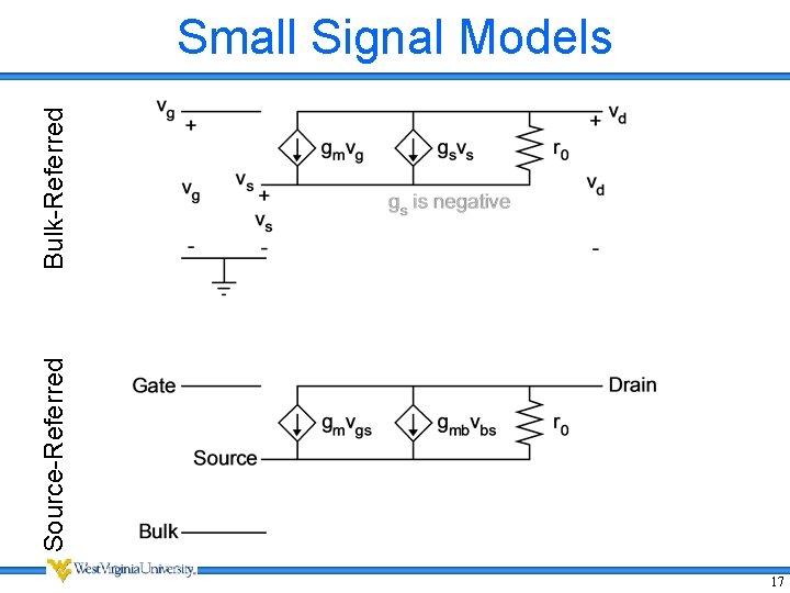
Bulk Referred Small-Signal Model • Every potential is with respect to (wrt) the bulk • Use VCCS to model changes in current from DC • No gate current • Increases in the gate & drain wrt the bulk increase the channel current (drain-to-source) • Increases in the source wrt the bulk decrease the channel current Total Current (centered around IBIAS) 6

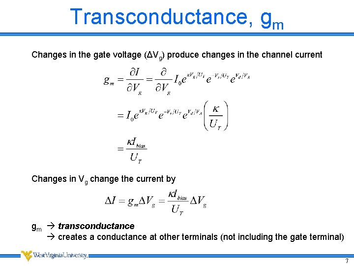
Transconductance, gm Changes in the gate voltage (ΔVg) produce changes in the channel current Changes in Vg change the current by gm transconductance creates a conductance at other terminals (not including the gate terminal) 7

Bulk-Referred Small-Signal Model • Derive the small signal parameters for subthreshold operation – gm – gs – gd • Bulk-referred model is typically used for subthreshold modeling • (Source-referred model is typically used for above threshold modeling) 8

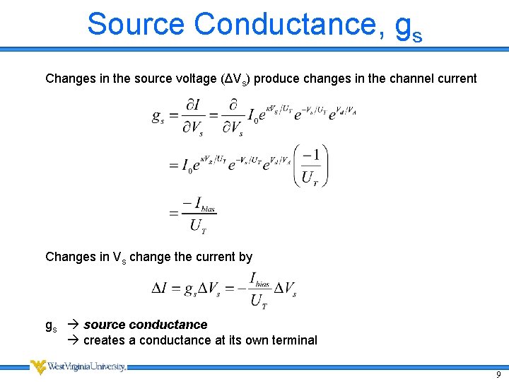
Source Conductance, gs Changes in the source voltage (ΔVs) produce changes in the channel current Changes in Vs change the current by gs source conductance creates a conductance at its own terminal 9

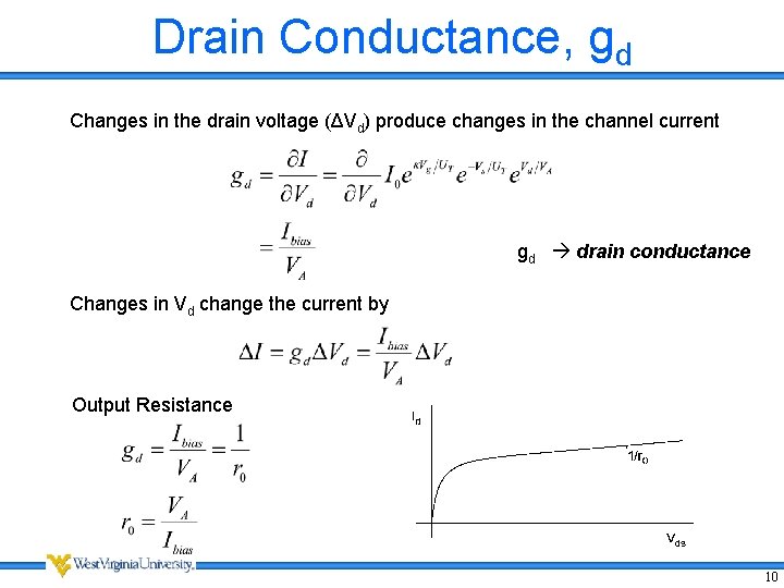
Drain Conductance, gd Changes in the drain voltage (ΔVd) produce changes in the channel current gd drain conductance Changes in Vd change the current by Output Resistance 10

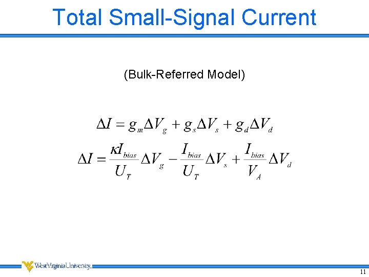
Total Small-Signal Current (Bulk-Referred Model) 11

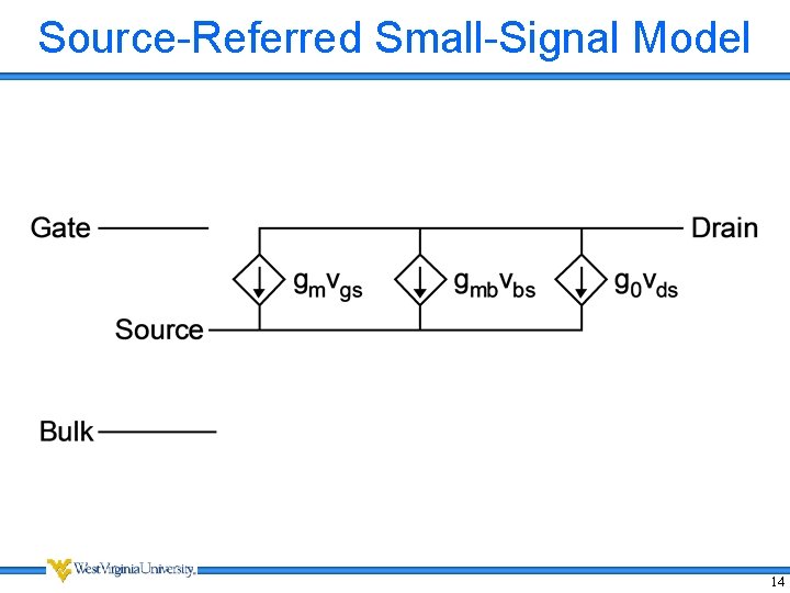
Source-Referred Small-Signal Model (Low Frequency) 12

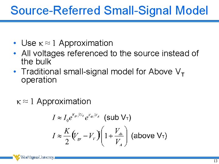
Source-Referred Small-Signal Model • Use κ ≈ 1 Approximation • All voltages referenced to the source instead of the bulk • Traditional small-signal model for Above VT operation κ ≈ 1 Approximation 13

Source-Referred Small-Signal Model 14

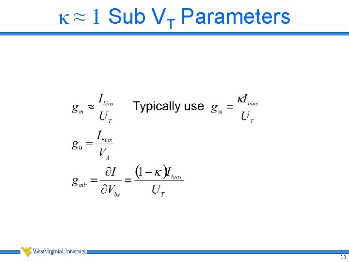
κ ≈ 1 Sub VT Parameters 15

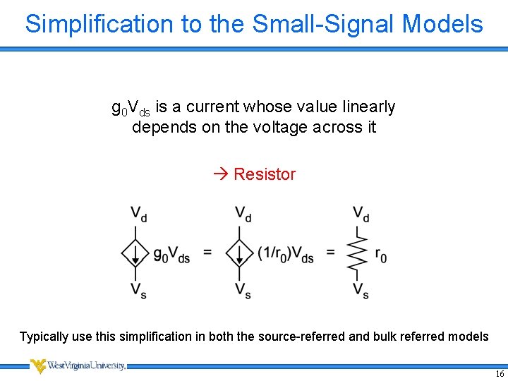
Simplification to the Small-Signal Models g 0 Vds is a current whose value linearly depends on the voltage across it Resistor Typically use this simplification in both the source-referred and bulk referred models 16

Source-Referred Bulk-Referred Small Signal Models 17

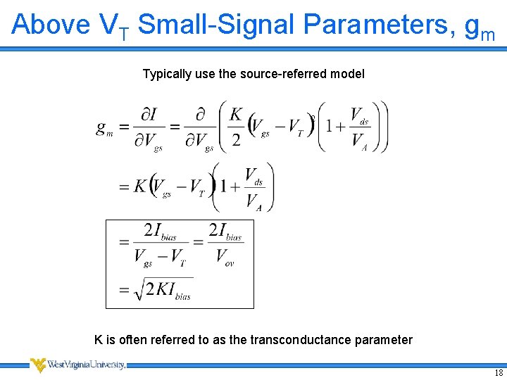
Above VT Small-Signal Parameters, gm Typically use the source-referred model K is often referred to as the transconductance parameter 18

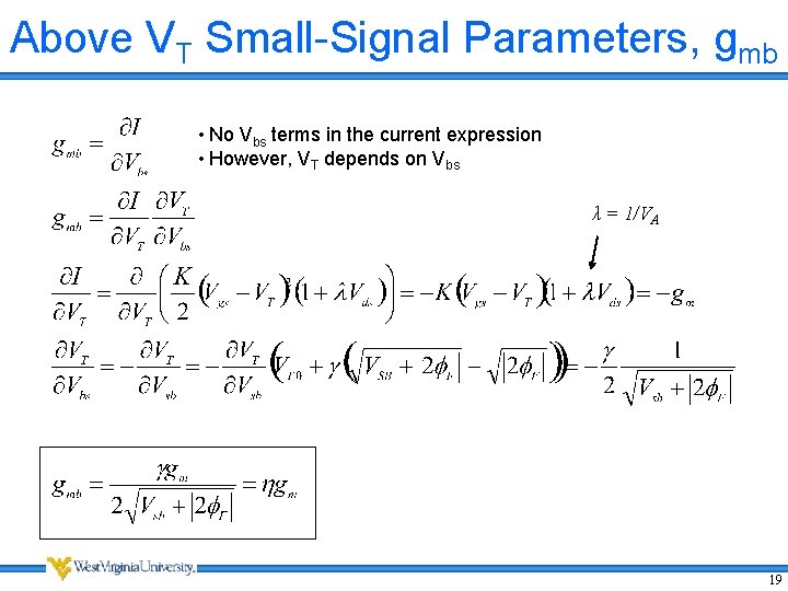
Above VT Small-Signal Parameters, gmb • No Vbs terms in the current expression • However, VT depends on Vbs λ = 1/VA 19

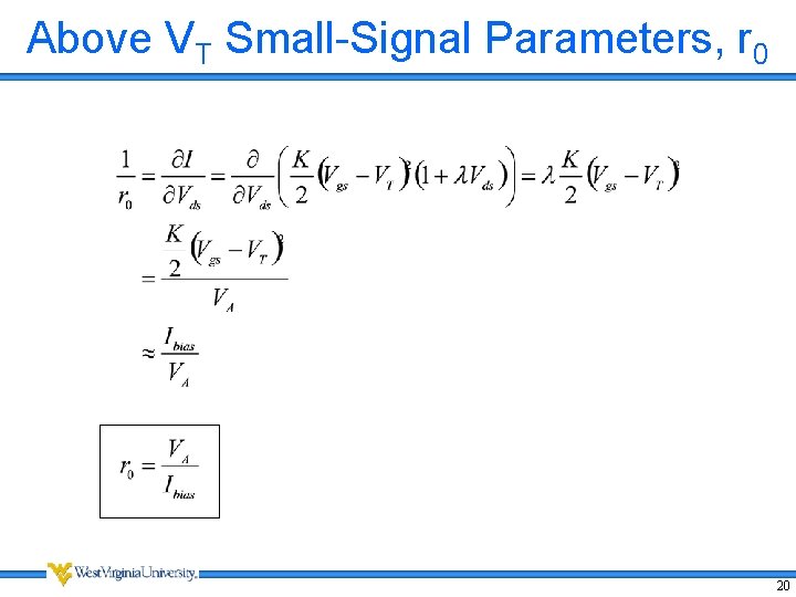
Above VT Small-Signal Parameters, r 0 20

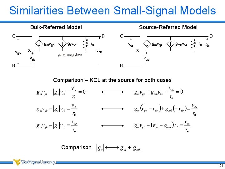
Similarities Between Small-Signal Models Bulk-Referred Model Source-Referred Model Comparison – KCL at the source for both cases Comparison 21

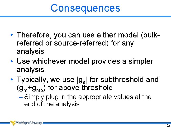
Consequences • Therefore, you can use either model (bulkreferred or source-referred) for any analysis • Use whichever model provides a simpler analysis • Typically, we use |gs| for subthreshold and (gm+gmb) for above threshold – Simply plug in the appropriate values at the end of the analysis 22

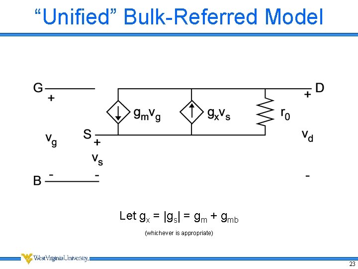
“Unified” Bulk-Referred Model Let gx = |gs| = gm + gmb (whichever is appropriate) 23

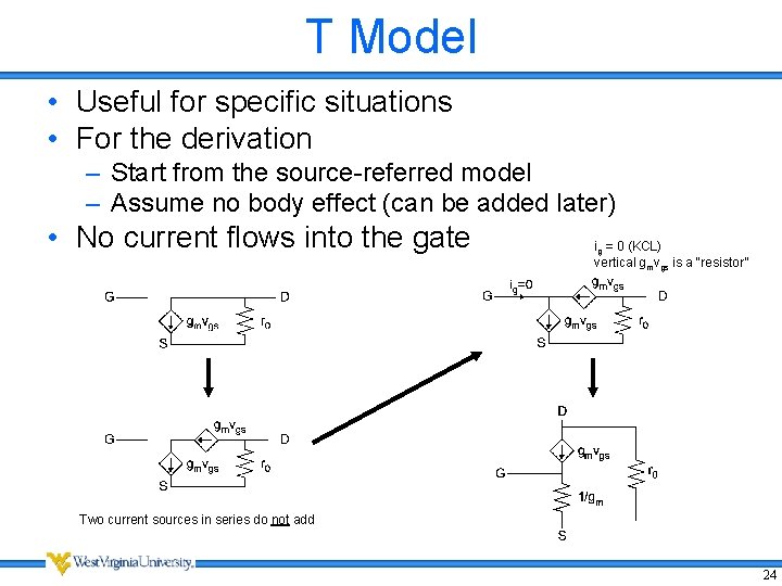
T Model • Useful for specific situations • For the derivation – Start from the source-referred model – Assume no body effect (can be added later) • No current flows into the gate ig = 0 (KCL) vertical gmvgs is a “resistor” Two current sources in series do not add 24

Exploring the Small-Signal Parameters 25

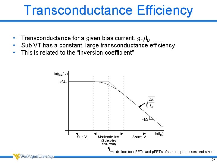
Transconductance Efficiency • Transconductance for a given bias current, gm/ID • Sub VT has a constant, large transconductance efficiency • This is related to the “inversion coefficient” Holds true for n. FETs and p. FETs of various processes and sizes 26

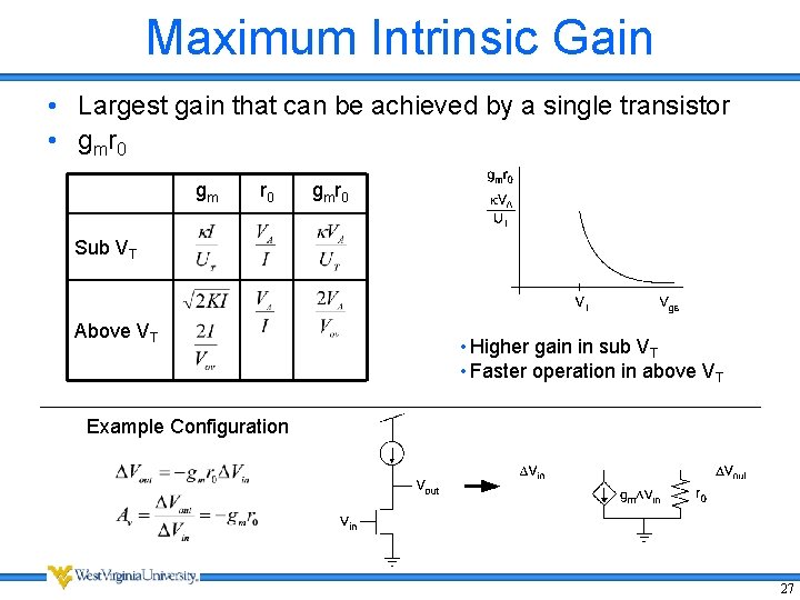
Maximum Intrinsic Gain • Largest gain that can be achieved by a single transistor • g mr 0 gmr 0 Sub VT Above VT • Higher gain in sub VT • Faster operation in above VT Example Configuration 27