SmallSignal Differential Amplifier Operation Chris Allen calleneecs ku
- Slides: 78

Small-Signal Differential Amplifier Operation Chris Allen (callen@eecs. ku. edu) Course website URL people. eecs. ku. edu/~callen/412/EECS 412. htm 1

Outline Differential amplifier overview BJT differential pair Small-signal characteristics of differential BJT amplifier Current sources and current mirrors Active loads Multistage Op Amp Circuit 741 Op Amp Circuit 2

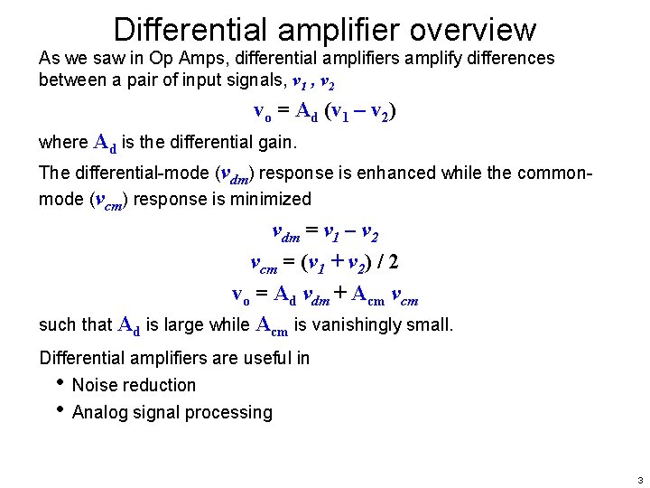
Differential amplifier overview As we saw in Op Amps, differential amplifiers amplify differences between a pair of input signals, v 1 , v 2 vo = Ad (v 1 – v 2) where Ad is the differential gain. The differential-mode (vdm) response is enhanced while the commonmode (vcm) response is minimized vdm = v 1 – v 2 vcm = (v 1 + v 2) / 2 vo = Ad vdm + Acm vcm such that Ad is large while Acm is vanishingly small. Differential amplifiers are useful in • Noise reduction • Analog signal processing 3

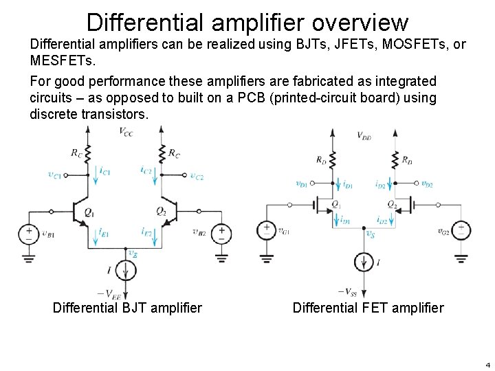
Differential amplifier overview Differential amplifiers can be realized using BJTs, JFETs, MOSFETs, or MESFETs. For good performance these amplifiers are fabricated as integrated circuits – as opposed to built on a PCB (printed-circuit board) using discrete transistors. Differential BJT amplifier Differential FET amplifier 4

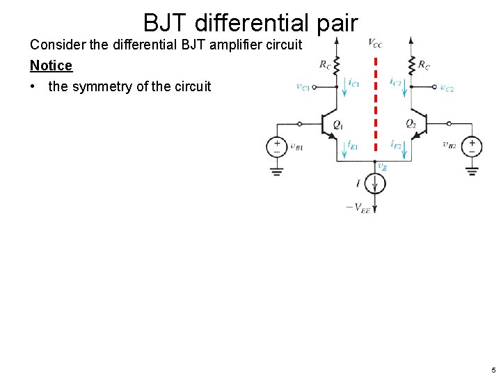
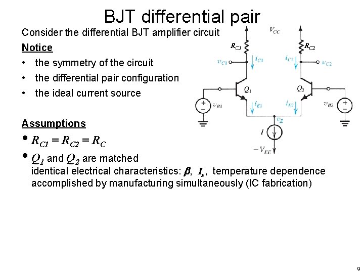
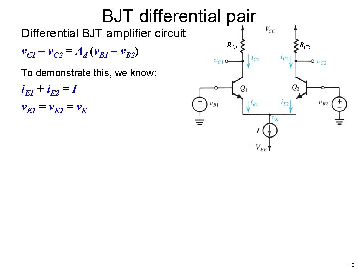
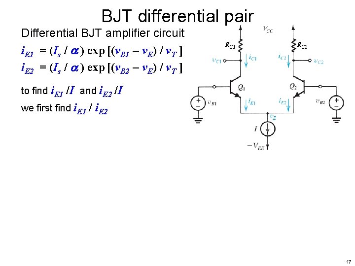
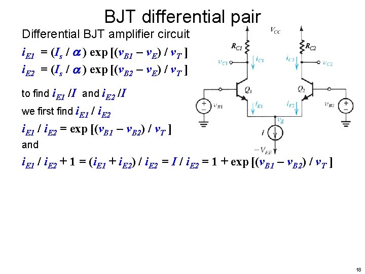
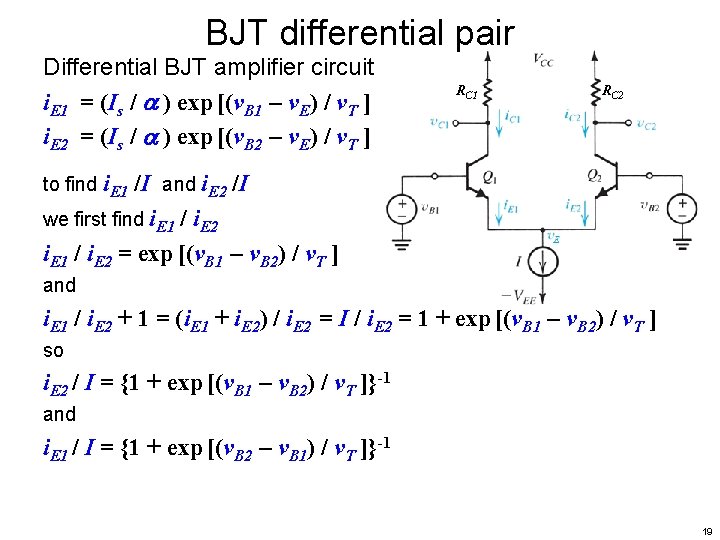
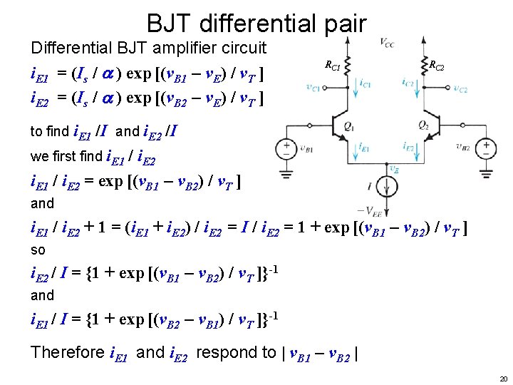
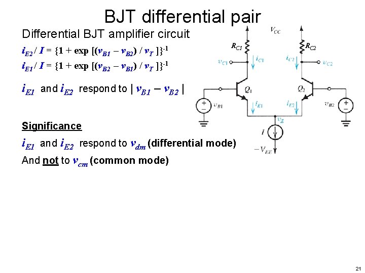
BJT differential pair Consider the differential BJT amplifier circuit Notice • the symmetry of the circuit 5

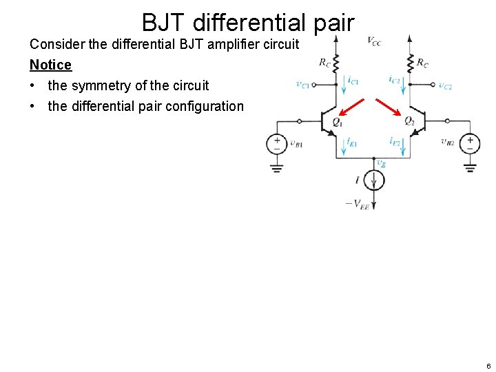
BJT differential pair Consider the differential BJT amplifier circuit Notice • the symmetry of the circuit • the differential pair configuration 6

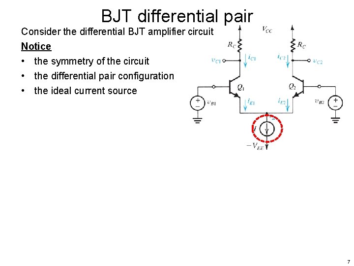
BJT differential pair Consider the differential BJT amplifier circuit Notice • the symmetry of the circuit • the differential pair configuration • the ideal current source 7

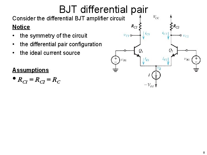
BJT differential pair Consider the differential BJT amplifier circuit Notice RC 1 RC 2 • the symmetry of the circuit • the differential pair configuration • the ideal current source Assumptions • RC 1 = RC 2 = RC 8

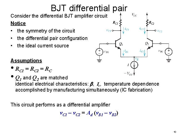
BJT differential pair Consider the differential BJT amplifier circuit Notice RC 1 RC 2 • the symmetry of the circuit • the differential pair configuration • the ideal current source Assumptions • RC 1 = RC 2 = RC • Q 1 and Q 2 are matched identical electrical characteristics: , Is, temperature dependence accomplished by manufacturing simultaneously (IC fabrication) 9

BJT differential pair Consider the differential BJT amplifier circuit Notice RC 1 RC 2 • the symmetry of the circuit • the differential pair configuration • the ideal current source Assumptions • RC 1 = RC 2 = RC • Q 1 and Q 2 are matched identical electrical characteristics: , Is, temperature dependence accomplished by manufacturing simultaneously (IC fabrication) This circuit performs as a differential amplifier v. C 1 – v. C 2 = Ad (v. B 1 – v. B 2) 10

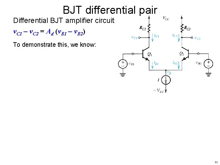
BJT differential pair Differential BJT amplifier circuit v. C 1 – v. C 2 = Ad (v. B 1 – v. B 2) RC 1 RC 2 To demonstrate this, we know: 11

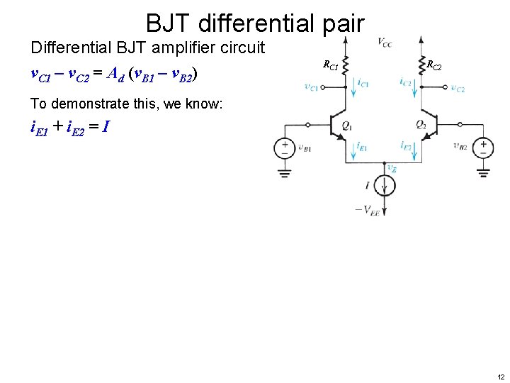
BJT differential pair Differential BJT amplifier circuit v. C 1 – v. C 2 = Ad (v. B 1 – v. B 2) RC 1 RC 2 To demonstrate this, we know: i. E 1 + i. E 2 = I 12

BJT differential pair Differential BJT amplifier circuit v. C 1 – v. C 2 = Ad (v. B 1 – v. B 2) RC 1 RC 2 To demonstrate this, we know: i. E 1 + i. E 2 = I v. E 1 = v. E 2 = v. E 13

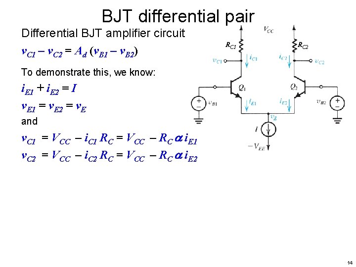
BJT differential pair Differential BJT amplifier circuit v. C 1 – v. C 2 = Ad (v. B 1 – v. B 2) RC 1 RC 2 To demonstrate this, we know: i. E 1 + i. E 2 = I v. E 1 = v. E 2 = v. E and v. C 1 = VCC – i. C 1 RC = VCC – RC i. E 1 v. C 2 = VCC – i. C 2 RC = VCC – RC i. E 2 14

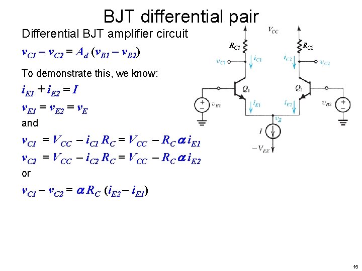
BJT differential pair Differential BJT amplifier circuit v. C 1 – v. C 2 = Ad (v. B 1 – v. B 2) RC 1 RC 2 To demonstrate this, we know: i. E 1 + i. E 2 = I v. E 1 = v. E 2 = v. E and v. C 1 = VCC – i. C 1 RC = VCC – RC i. E 1 v. C 2 = VCC – i. C 2 RC = VCC – RC i. E 2 or v. C 1 – v. C 2 = RC (i. E 2 – i. E 1) 15

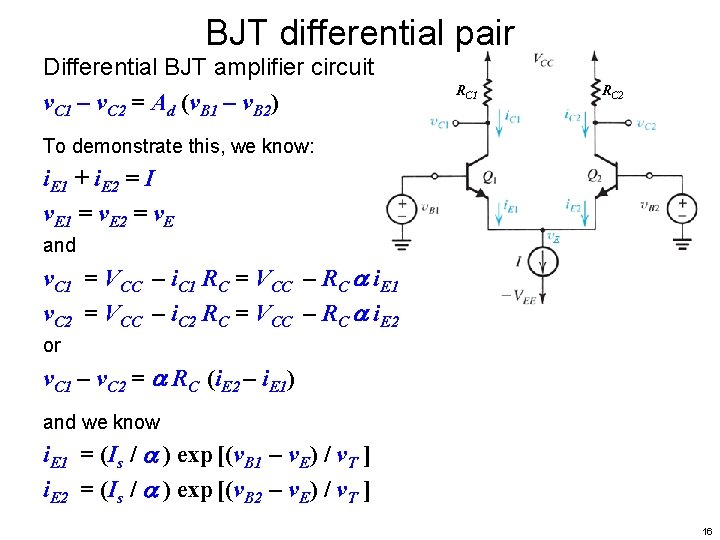
BJT differential pair Differential BJT amplifier circuit v. C 1 – v. C 2 = Ad (v. B 1 – v. B 2) RC 1 RC 2 To demonstrate this, we know: i. E 1 + i. E 2 = I v. E 1 = v. E 2 = v. E and v. C 1 = VCC – i. C 1 RC = VCC – RC i. E 1 v. C 2 = VCC – i. C 2 RC = VCC – RC i. E 2 or v. C 1 – v. C 2 = RC (i. E 2 – i. E 1) and we know i. E 1 = (Is / ) exp [(v. B 1 – v. E) / v. T ] i. E 2 = (Is / ) exp [(v. B 2 – v. E) / v. T ] 16

BJT differential pair Differential BJT amplifier circuit i. E 1 = (Is / ) exp [(v. B 1 – v. E) / v. T ] i. E 2 = (Is / ) exp [(v. B 2 – v. E) / v. T ] RC 1 RC 2 to find i. E 1 /I and i. E 2 /I we first find i. E 1 / i. E 2 17

BJT differential pair Differential BJT amplifier circuit i. E 1 = (Is / ) exp [(v. B 1 – v. E) / v. T ] i. E 2 = (Is / ) exp [(v. B 2 – v. E) / v. T ] RC 1 RC 2 to find i. E 1 /I and i. E 2 /I we first find i. E 1 / i. E 2 = exp [(v. B 1 – v. B 2) / v. T ] and i. E 1 / i. E 2 + 1 = (i. E 1 + i. E 2) / i. E 2 = I / i. E 2 = 1 + exp [(v. B 1 – v. B 2) / v. T ] 18

BJT differential pair Differential BJT amplifier circuit i. E 1 = (Is / ) exp [(v. B 1 – v. E) / v. T ] i. E 2 = (Is / ) exp [(v. B 2 – v. E) / v. T ] RC 1 RC 2 to find i. E 1 /I and i. E 2 /I we first find i. E 1 / i. E 2 = exp [(v. B 1 – v. B 2) / v. T ] and i. E 1 / i. E 2 + 1 = (i. E 1 + i. E 2) / i. E 2 = I / i. E 2 = 1 + exp [(v. B 1 – v. B 2) / v. T ] so i. E 2 / I = {1 + exp [(v. B 1 – v. B 2) / v. T ]}-1 and i. E 1 / I = {1 + exp [(v. B 2 – v. B 1) / v. T ]}-1 19

BJT differential pair Differential BJT amplifier circuit i. E 1 = (Is / ) exp [(v. B 1 – v. E) / v. T ] i. E 2 = (Is / ) exp [(v. B 2 – v. E) / v. T ] RC 1 RC 2 to find i. E 1 /I and i. E 2 /I we first find i. E 1 / i. E 2 = exp [(v. B 1 – v. B 2) / v. T ] and i. E 1 / i. E 2 + 1 = (i. E 1 + i. E 2) / i. E 2 = I / i. E 2 = 1 + exp [(v. B 1 – v. B 2) / v. T ] so i. E 2 / I = {1 + exp [(v. B 1 – v. B 2) / v. T ]}-1 and i. E 1 / I = {1 + exp [(v. B 2 – v. B 1) / v. T ]}-1 Therefore i. E 1 and i. E 2 respond to | v. B 1 – v. B 2 | 20

BJT differential pair Differential BJT amplifier circuit i. E 2 / I = {1 + exp [(v. B 1 – v. B 2) / v. T ]}-1 i. E 1 / I = {1 + exp [(v. B 2 – v. B 1) / v. T ]}-1 RC 2 i. E 1 and i. E 2 respond to | v. B 1 – v. B 2 | Significance i. E 1 and i. E 2 respond to vdm (differential mode) And not to vcm (common mode) 21

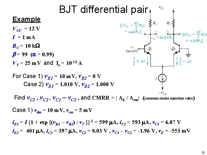
BJT differential pair Example VCC = 12 V I = 1 m. A RC = 10 k = 99 ( = 0. 99) VT = 25 m. V and Is = 10 -13 A For Case 1) v. B 1 = 10 m. V, v. B 2 = 0 V Case 2) v. B 1 = 1. 010 V, v. B 2 = 1. 000 V Find v. C 1 , v. C 2 , v. C 1 – v. C 2 , and CMRR = | Ad / Acm| (common-mode rejection ratio) Case 1) vdm = 10 m. V, vcm = 5 m. V i. E 1 = I {1 + exp [(v. B 1 – v. B 2) / v. T ]}-1 = 599 A, i. C 1 = 593 A, v. C 1 = 6. 07 V i. E 2 = 401 A, i. C 2 = 397 A, v. C 2 = 8. 03 V , v. C 1 – v. C 2 = -1. 96 V, v. E = -553 m. V 22

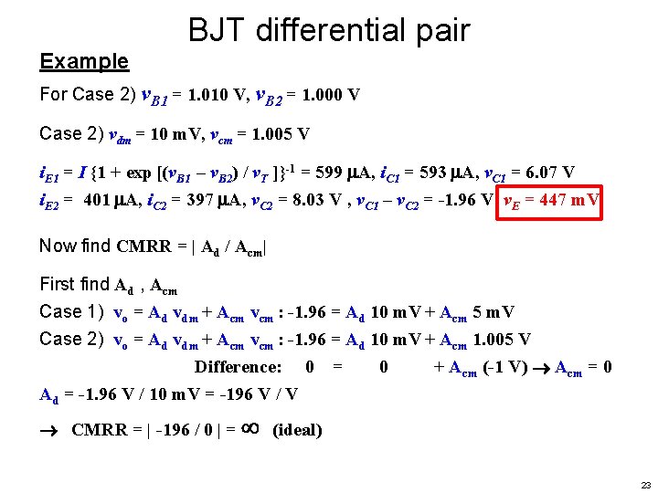
BJT differential pair Example For Case 2) v. B 1 = 1. 010 V, v. B 2 = 1. 000 V Case 2) vdm = 10 m. V, vcm = 1. 005 V i. E 1 = I {1 + exp [(v. B 1 – v. B 2) / v. T ]}-1 = 599 A, i. C 1 = 593 A, v. C 1 = 6. 07 V i. E 2 = 401 A, i. C 2 = 397 A, v. C 2 = 8. 03 V , v. C 1 – v. C 2 = -1. 96 V, v. E = 447 m. V Now find CMRR = | Ad / Acm| First find Ad , Acm Case 1) vo = Ad vdm + Acm vcm : -1. 96 = Ad 10 m. V + Acm 5 m. V Case 2) vo = Ad vdm + Acm vcm : -1. 96 = Ad 10 m. V + Acm 1. 005 V Difference: 0 = 0 + Acm (-1 V) Acm = 0 Ad = -1. 96 V / 10 m. V = -196 V / V CMRR = | -196 / 0 | = (ideal) 23

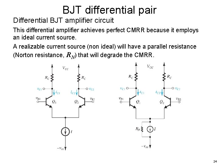
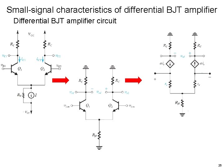
BJT differential pair Differential BJT amplifier circuit This differential amplifier achieves perfect CMRR because it employs an ideal current source. A realizable current source (non ideal) will have a parallel resistance (Norton resistance, RN) that will degrade the CMRR. 24

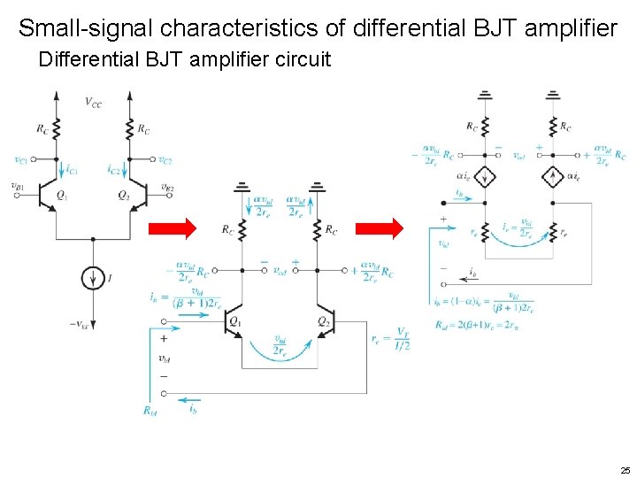
Small-signal characteristics of differential BJT amplifier Differential BJT amplifier circuit 25

Small-signal characteristics of differential BJT amplifier Differential BJT amplifier circuit 26

Current sources and current mirrors Differential amplifier biasing Motivation Just as with BJT and FET amplifiers, biasing to achieve constant bias current is important in differential amplifiers as well. Differential amplifiers structures we’ve looked at are biased using independent current sources. As we study various circuits that act as current sources for biasing these circuits we know they must provide: • a stable current source • a large Norton equivalent resistance Throughout this study we will assume the BJTs will be in active mode, FETs will be in saturation mode. 27

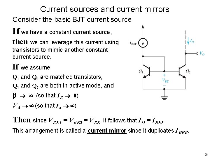
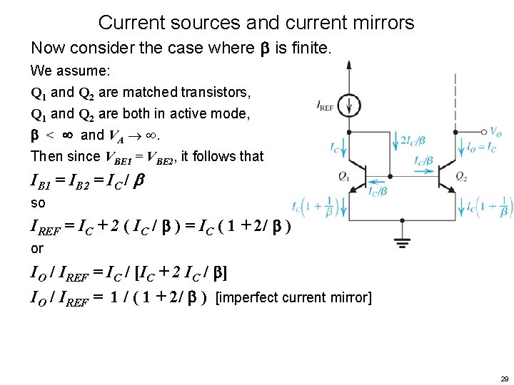
Current sources and current mirrors Consider the basic BJT current source If we have a constant current source, then we can leverage this current using transistors to mimic another constant current source. If we assume: Q 1 and Q 2 are matched transistors, Q 1 and Q 2 are both in active mode, and (so that IB 0) VA (so that ro ) Then since VBE 1 = VBE 2 = VBE, it follows that IO = IREF This arrangement is called a current mirror since it duplicates IREF. 28

Current sources and current mirrors Now consider the case where is finite. We assume: Q 1 and Q 2 are matched transistors, Q 1 and Q 2 are both in active mode, < and VA . Then since VBE 1 = VBE 2, it follows that IB 1 = IB 2 = IC / so IREF = IC + 2 ( IC / ) = IC ( 1 + 2/ ) or IO / IREF = IC / [IC + 2 IC / ] IO / IREF = 1 / ( 1 + 2/ ) [imperfect current mirror] 29

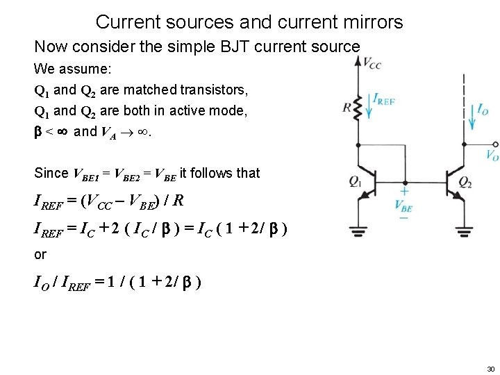
Current sources and current mirrors Now consider the simple BJT current source We assume: Q 1 and Q 2 are matched transistors, Q 1 and Q 2 are both in active mode, < and VA . Since VBE 1 = VBE 2 = VBE it follows that IREF = (VCC – VBE) / R IREF = IC + 2 ( IC / ) = IC ( 1 + 2/ ) or IO / IREF = 1 / ( 1 + 2/ ) 30

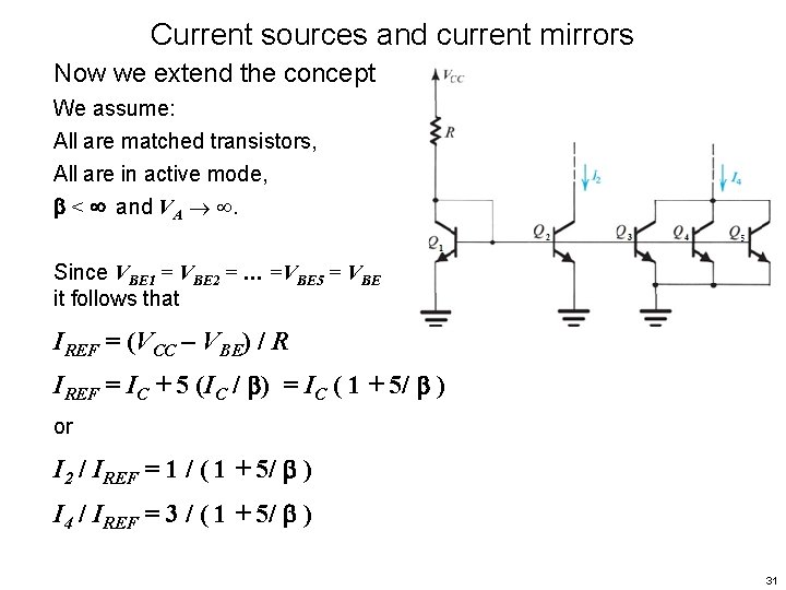
Current sources and current mirrors Now we extend the concept We assume: All are matched transistors, All are in active mode, < and VA . Since VBE 1 = VBE 2 = … =VBE 5 = VBE it follows that IREF = (VCC – VBE) / R IREF = IC + 5 (IC / ) = IC ( 1 + 5/ ) or I 2 / IREF = 1 / ( 1 + 5/ ) I 4 / IREF = 3 / ( 1 + 5/ ) 31

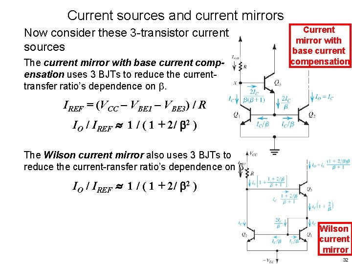
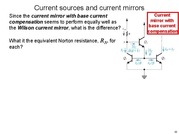
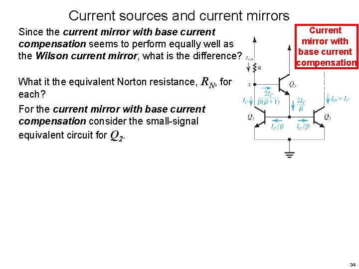
Current sources and current mirrors Now consider these 3 -transistor current sources The current mirror with base current compensation uses 3 BJTs to reduce the currenttransfer ratio’s dependence on . Current mirror with base current compensation IREF = (VCC – VBE 1 – VBE 3) / R IO / IREF 1 / ( 1 + 2/ 2 ) The Wilson current mirror also uses 3 BJTs to reduce the current-ransfer ratio’s dependence on . IO / IREF 1 / ( 1 + 2/ 2 ) Wilson current mirror 32

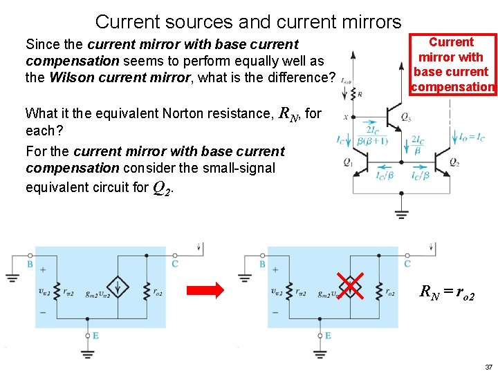
Current sources and current mirrors Since the current mirror with base current compensation seems to perform equally well as the Wilson current mirror, what is the difference? Current mirror with base current compensation What it the equivalent Norton resistance, RN, for each? 33

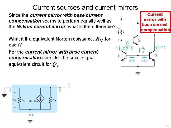
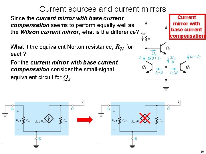
Current sources and current mirrors Since the current mirror with base current compensation seems to perform equally well as the Wilson current mirror, what is the difference? Current mirror with base current compensation What it the equivalent Norton resistance, RN, for each? For the current mirror with base current compensation consider the small-signal equivalent circuit for Q 2. 34

Current sources and current mirrors Since the current mirror with base current compensation seems to perform equally well as the Wilson current mirror, what is the difference? Current mirror with base current compensation What it the equivalent Norton resistance, RN, for each? For the current mirror with base current compensation consider the small-signal equivalent circuit for Q 2. 35

Current sources and current mirrors Since the current mirror with base current compensation seems to perform equally well as the Wilson current mirror, what is the difference? Current mirror with base current compensation What it the equivalent Norton resistance, RN, for each? For the current mirror with base current compensation consider the small-signal equivalent circuit for Q 2. 36

Current sources and current mirrors Since the current mirror with base current compensation seems to perform equally well as the Wilson current mirror, what is the difference? Current mirror with base current compensation What it the equivalent Norton resistance, RN, for each? For the current mirror with base current compensation consider the small-signal equivalent circuit for Q 2. RN = ro 2 37

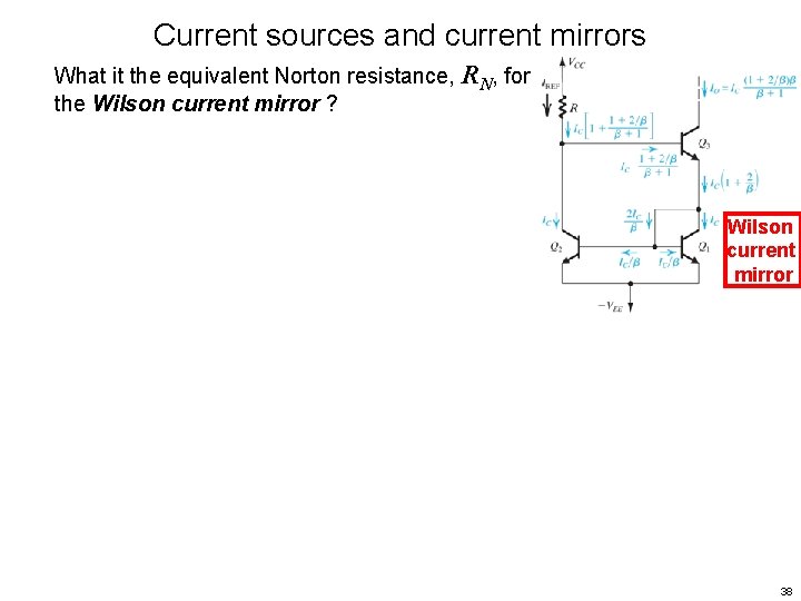
Current sources and current mirrors What it the equivalent Norton resistance, RN, for the Wilson current mirror ? Wilson current mirror 38

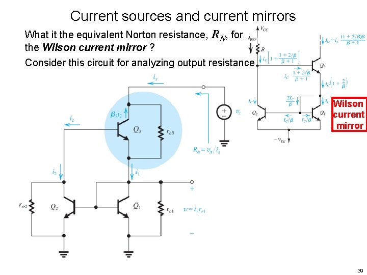
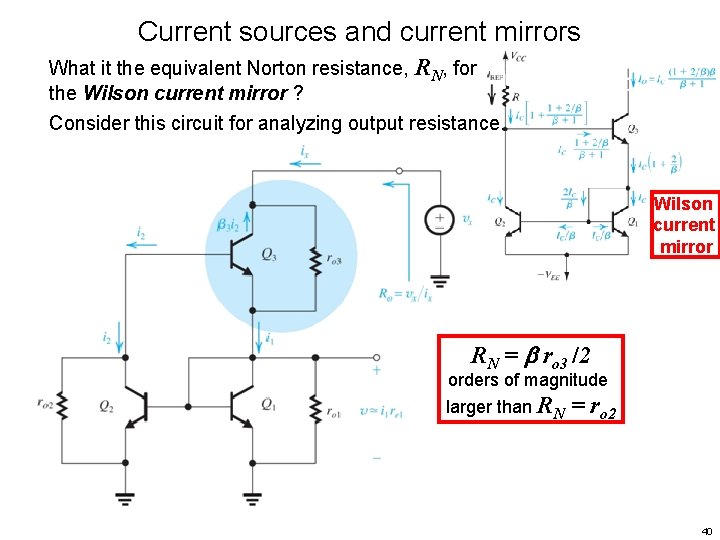
Current sources and current mirrors What it the equivalent Norton resistance, RN, for the Wilson current mirror ? Consider this circuit for analyzing output resistance. Wilson current mirror 39

Current sources and current mirrors What it the equivalent Norton resistance, RN, for the Wilson current mirror ? Consider this circuit for analyzing output resistance. Wilson current mirror RN = ro 3 /2 orders of magnitude larger than RN = ro 2 40

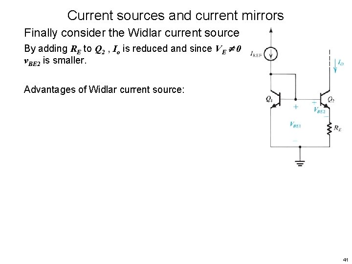
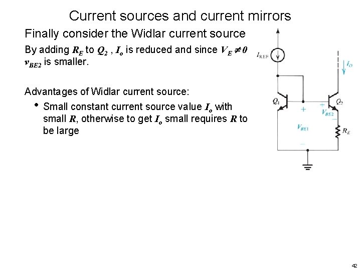
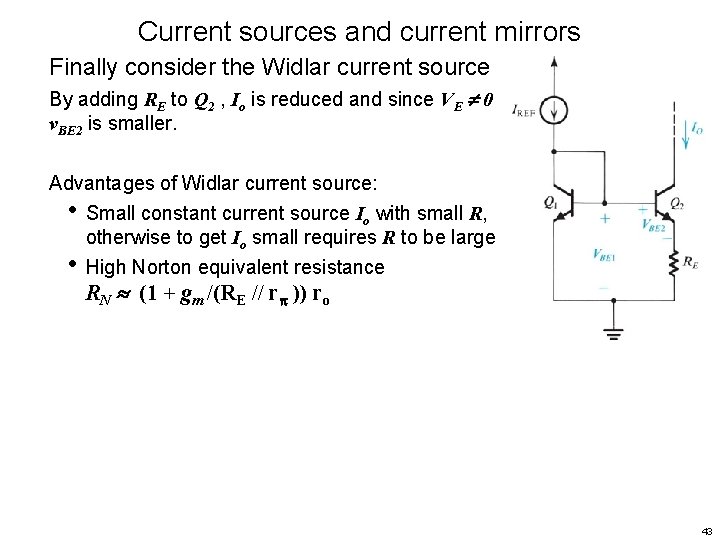
Current sources and current mirrors Finally consider the Widlar current source By adding RE to Q 2 , Io is reduced and since VE 0 v. BE 2 is smaller. Advantages of Widlar current source: 41

Current sources and current mirrors Finally consider the Widlar current source By adding RE to Q 2 , Io is reduced and since VE 0 v. BE 2 is smaller. Advantages of Widlar current source: • Small constant current source value Io with small R, otherwise to get Io small requires R to be large 42

Current sources and current mirrors Finally consider the Widlar current source By adding RE to Q 2 , Io is reduced and since VE 0 v. BE 2 is smaller. Advantages of Widlar current source: • Small constant current source Io with small R, otherwise to get Io small requires R to be large • High Norton equivalent resistance RN (1 + gm /(RE // r )) ro 43

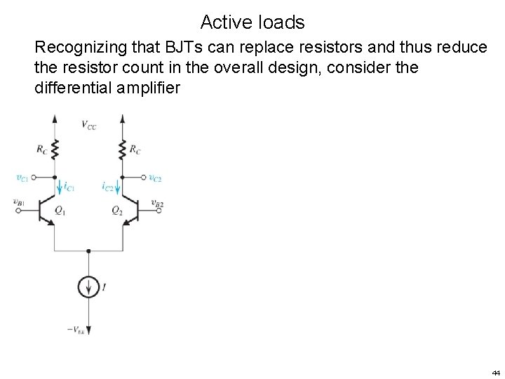
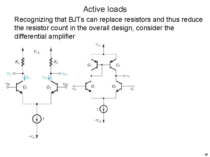
Active loads Recognizing that BJTs can replace resistors and thus reduce the resistor count in the overall design, consider the differential amplifier 44

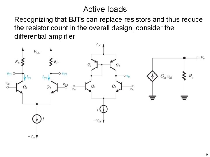
Active loads Recognizing that BJTs can replace resistors and thus reduce the resistor count in the overall design, consider the differential amplifier 45

Active loads Recognizing that BJTs can replace resistors and thus reduce the resistor count in the overall design, consider the differential amplifier 46

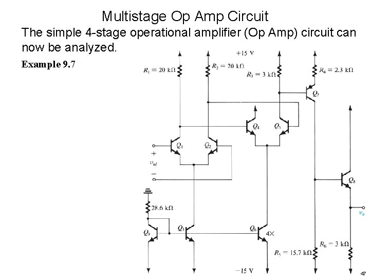
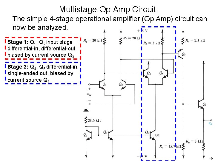
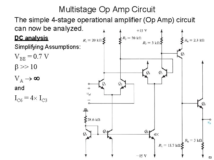
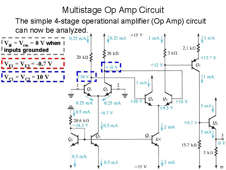
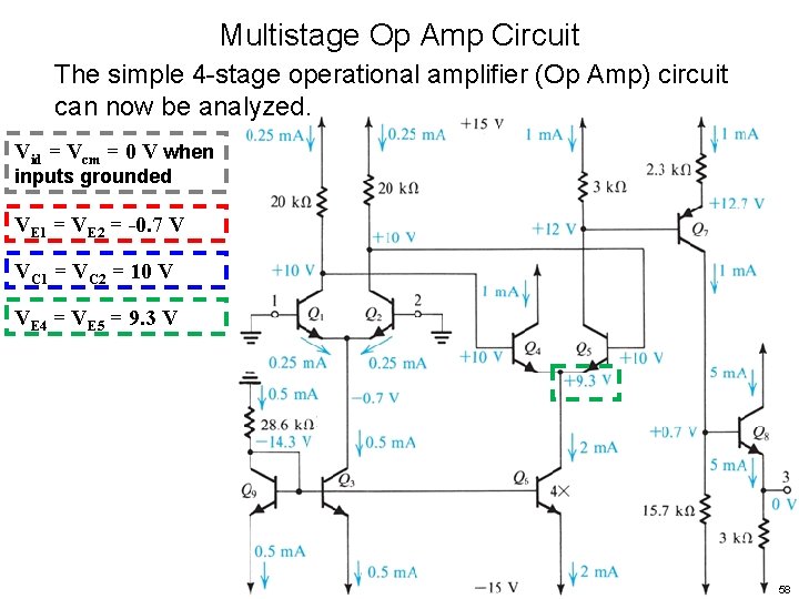
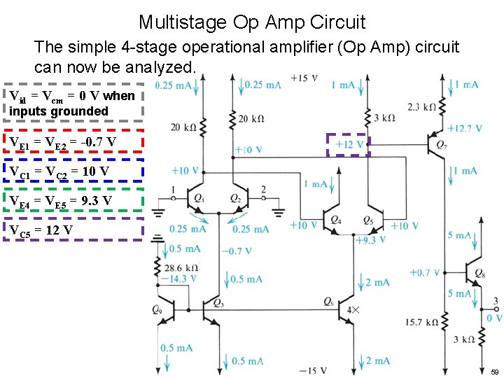
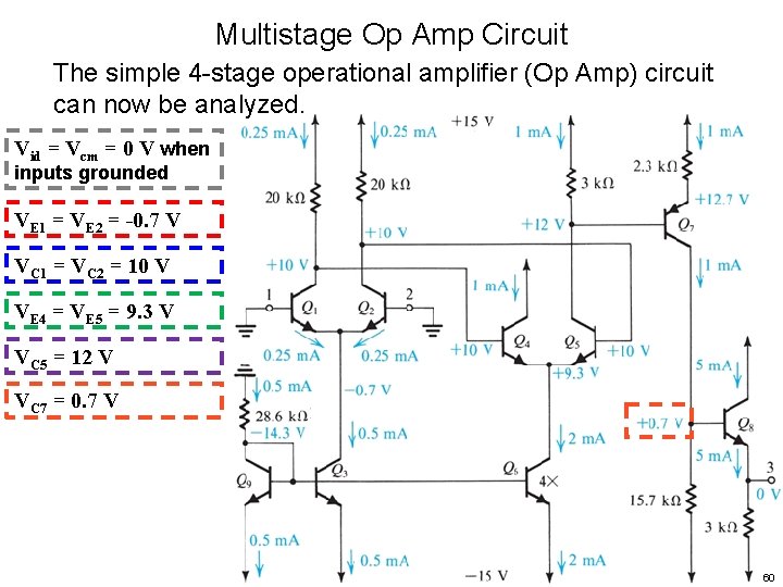
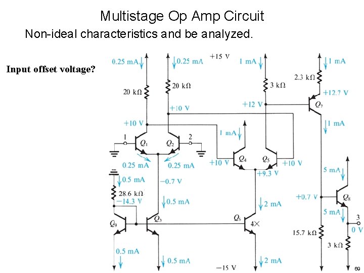
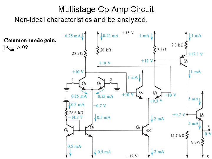
Multistage Op Amp Circuit The simple 4 -stage operational amplifier (Op Amp) circuit can now be analyzed. Example 9. 7 47

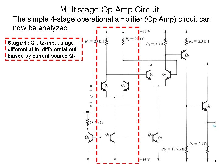
Multistage Op Amp Circuit The simple 4 -stage operational amplifier (Op Amp) circuit can now be analyzed. Stage 1: Q 1, Q 2 input stage differential-in, differential-out biased by current source Q 3 48

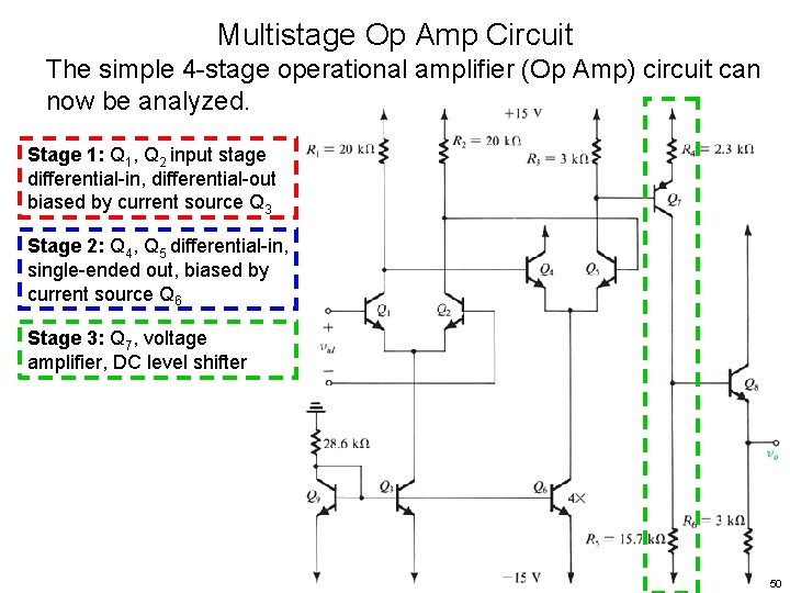
Multistage Op Amp Circuit The simple 4 -stage operational amplifier (Op Amp) circuit can now be analyzed. Stage 1: Q 1, Q 2 input stage differential-in, differential-out biased by current source Q 3 Stage 2: Q 4, Q 5 differential-in, single-ended out, biased by current source Q 6 49

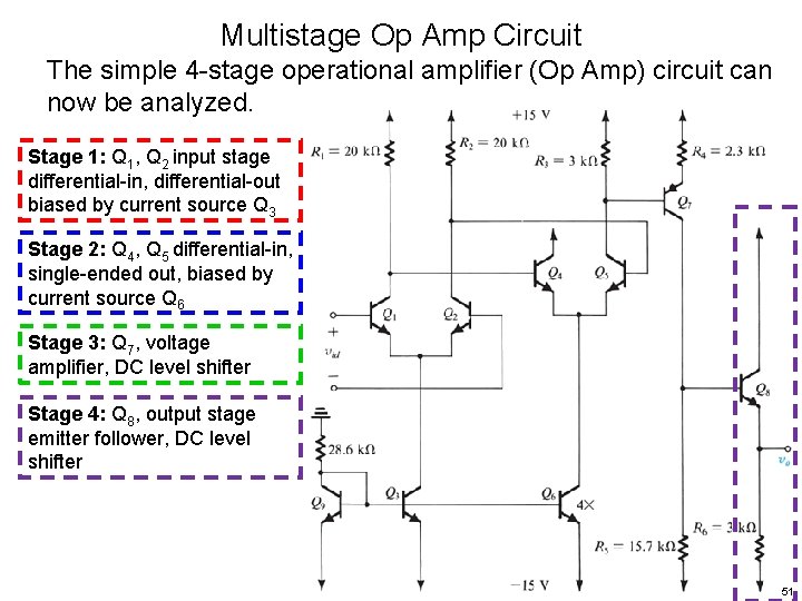
Multistage Op Amp Circuit The simple 4 -stage operational amplifier (Op Amp) circuit can now be analyzed. Stage 1: Q 1, Q 2 input stage differential-in, differential-out biased by current source Q 3 Stage 2: Q 4, Q 5 differential-in, single-ended out, biased by current source Q 6 Stage 3: Q 7, voltage amplifier, DC level shifter 50

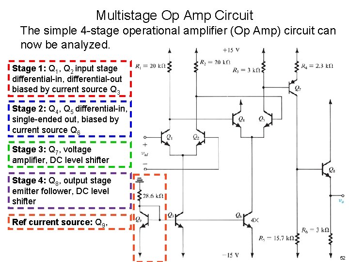
Multistage Op Amp Circuit The simple 4 -stage operational amplifier (Op Amp) circuit can now be analyzed. Stage 1: Q 1, Q 2 input stage differential-in, differential-out biased by current source Q 3 Stage 2: Q 4, Q 5 differential-in, single-ended out, biased by current source Q 6 Stage 3: Q 7, voltage amplifier, DC level shifter Stage 4: Q 8, output stage emitter follower, DC level shifter 51

Multistage Op Amp Circuit The simple 4 -stage operational amplifier (Op Amp) circuit can now be analyzed. Stage 1: Q 1, Q 2 input stage differential-in, differential-out biased by current source Q 3 Stage 2: Q 4, Q 5 differential-in, single-ended out, biased by current source Q 6 Stage 3: Q 7, voltage amplifier, DC level shifter Stage 4: Q 8, output stage emitter follower, DC level shifter Ref current source: Q 9, 52

Multistage Op Amp Circuit The simple 4 -stage operational amplifier (Op Amp) circuit can now be analyzed. DC analysis Simplifying Assumptions: VBE = 0. 7 V >> 10 VA and IC 6 = 4 IC 3 53

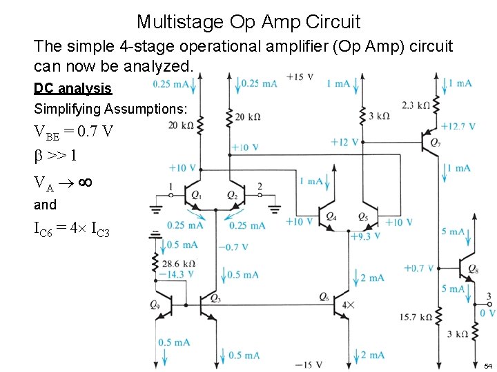
Multistage Op Amp Circuit The simple 4 -stage operational amplifier (Op Amp) circuit can now be analyzed. DC analysis Simplifying Assumptions: VBE = 0. 7 V >> 1 VA and IC 6 = 4 IC 3 54

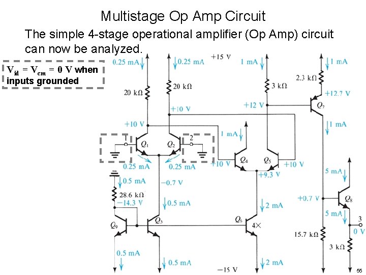
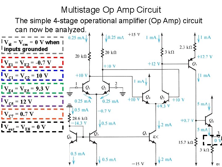
Multistage Op Amp Circuit The simple 4 -stage operational amplifier (Op Amp) circuit can now be analyzed. Vid = Vcm = 0 V when inputs grounded 55

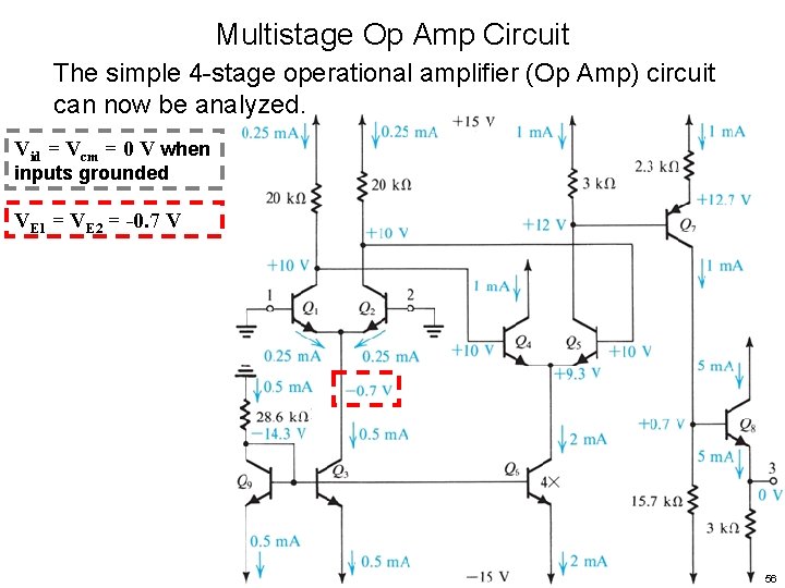
Multistage Op Amp Circuit The simple 4 -stage operational amplifier (Op Amp) circuit can now be analyzed. Vid = Vcm = 0 V when inputs grounded VE 1 = VE 2 = -0. 7 V 56

Multistage Op Amp Circuit The simple 4 -stage operational amplifier (Op Amp) circuit can now be analyzed. Vid = Vcm = 0 V when inputs grounded VE 1 = VE 2 = -0. 7 V VC 1 = VC 2 = 10 V 57

Multistage Op Amp Circuit The simple 4 -stage operational amplifier (Op Amp) circuit can now be analyzed. Vid = Vcm = 0 V when inputs grounded VE 1 = VE 2 = -0. 7 V VC 1 = VC 2 = 10 V VE 4 = VE 5 = 9. 3 V 58

Multistage Op Amp Circuit The simple 4 -stage operational amplifier (Op Amp) circuit can now be analyzed. Vid = Vcm = 0 V when inputs grounded VE 1 = VE 2 = -0. 7 V VC 1 = VC 2 = 10 V VE 4 = VE 5 = 9. 3 V VC 5 = 12 V 59

Multistage Op Amp Circuit The simple 4 -stage operational amplifier (Op Amp) circuit can now be analyzed. Vid = Vcm = 0 V when inputs grounded VE 1 = VE 2 = -0. 7 V VC 1 = VC 2 = 10 V VE 4 = VE 5 = 9. 3 V VC 5 = 12 V VC 7 = 0. 7 V 60

Multistage Op Amp Circuit The simple 4 -stage operational amplifier (Op Amp) circuit can now be analyzed. Vid = Vcm = 0 V when inputs grounded VE 1 = VE 2 = -0. 7 V VC 1 = VC 2 = 10 V VE 4 = VE 5 = 9. 3 V VC 5 = 12 V VC 7 = 0. 7 V Vout = VE 8 = 0 V 61

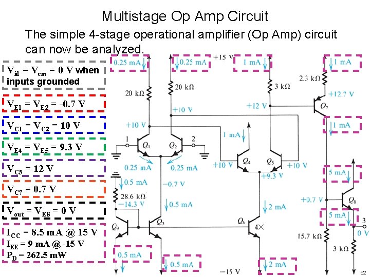
Multistage Op Amp Circuit The simple 4 -stage operational amplifier (Op Amp) circuit can now be analyzed. Vid = Vcm = 0 V when inputs grounded VE 1 = VE 2 = -0. 7 V VC 1 = VC 2 = 10 V VE 4 = VE 5 = 9. 3 V VC 5 = 12 V VC 7 = 0. 7 V Vout = VE 8 = 0 V ICC = 8. 5 m. A @ 15 V IEE = 9 m. A @ -15 V PD = 262. 5 m. W 62

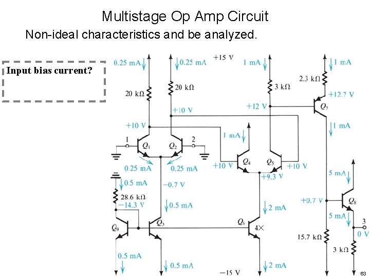
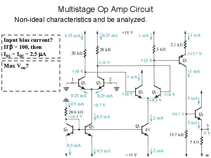
Multistage Op Amp Circuit Non-ideal characteristics and be analyzed. Input bias current? 63

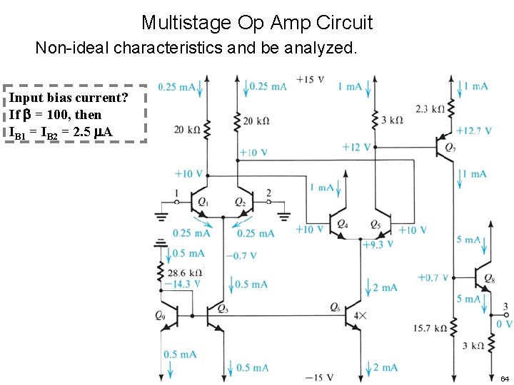
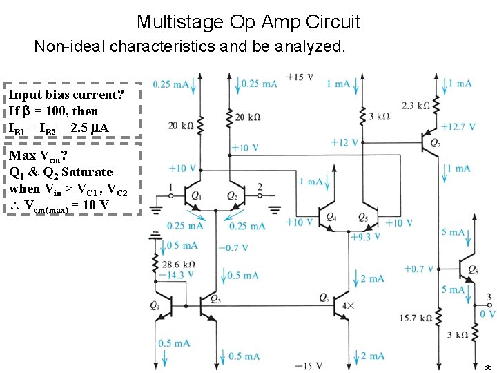
Multistage Op Amp Circuit Non-ideal characteristics and be analyzed. Input bias current? If = 100, then IB 1 = IB 2 = 2. 5 A 64

Multistage Op Amp Circuit Non-ideal characteristics and be analyzed. Input bias current? If = 100, then IB 1 = IB 2 = 2. 5 A Max Vcm? 65

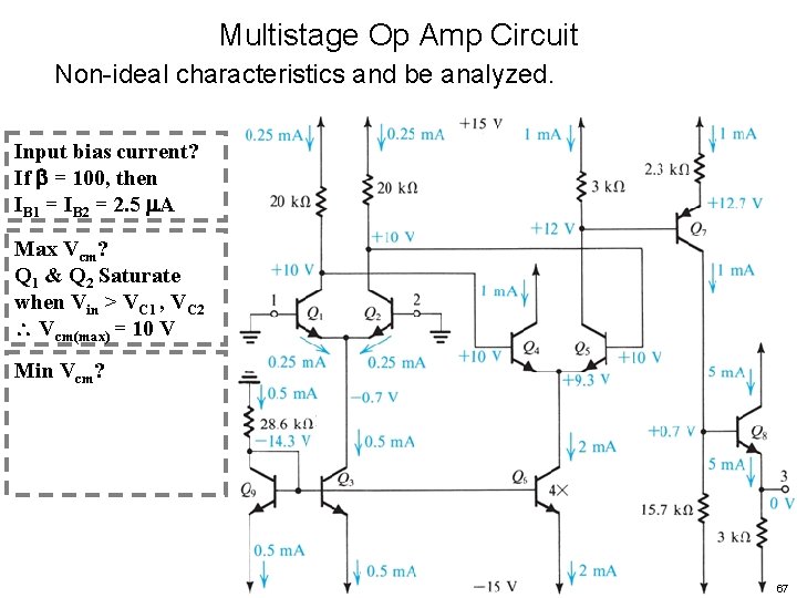
Multistage Op Amp Circuit Non-ideal characteristics and be analyzed. Input bias current? If = 100, then IB 1 = IB 2 = 2. 5 A Max Vcm? Q 1 & Q 2 Saturate when Vin > VC 1 , VC 2 Vcm(max) = 10 V 66

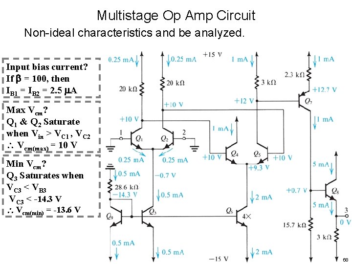
Multistage Op Amp Circuit Non-ideal characteristics and be analyzed. Input bias current? If = 100, then IB 1 = IB 2 = 2. 5 A Max Vcm? Q 1 & Q 2 Saturate when Vin > VC 1 , VC 2 Vcm(max) = 10 V Min Vcm? 67

Multistage Op Amp Circuit Non-ideal characteristics and be analyzed. Input bias current? If = 100, then IB 1 = IB 2 = 2. 5 A Max Vcm? Q 1 & Q 2 Saturate when Vin > VC 1 , VC 2 Vcm(max) = 10 V Min Vcm? Q 3 Saturates when VC 3 < VB 3 VC 3 < -14. 3 V Vcm(min) = -13. 6 V 68

Multistage Op Amp Circuit Non-ideal characteristics and be analyzed. Input offset voltage? 69

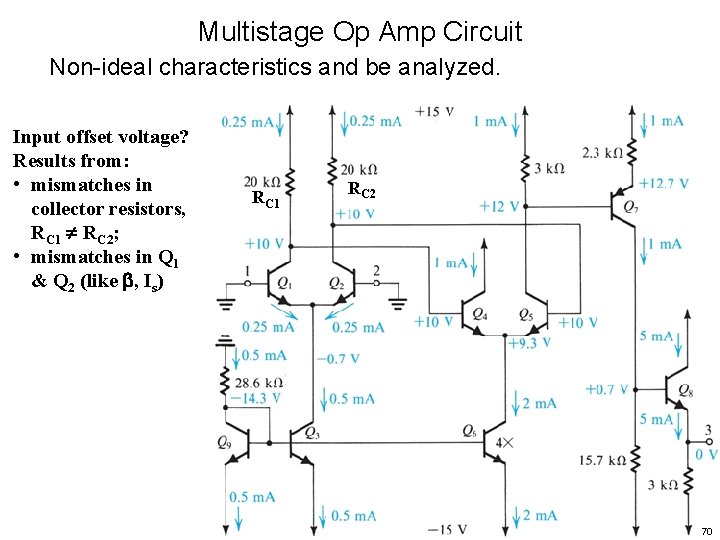
Multistage Op Amp Circuit Non-ideal characteristics and be analyzed. Input offset voltage? Results from: • mismatches in collector resistors, RC 1 RC 2; • mismatches in Q 1 & Q 2 (like , Is) RC 1 RC 2 70

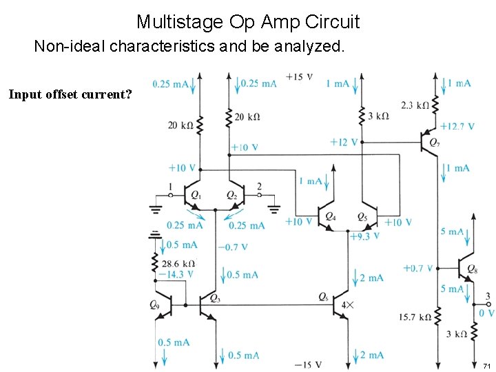
Multistage Op Amp Circuit Non-ideal characteristics and be analyzed. Input offset current? 71

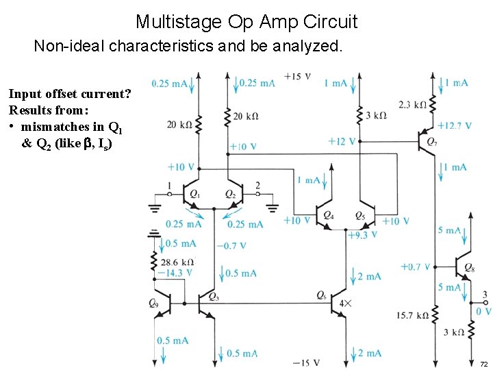
Multistage Op Amp Circuit Non-ideal characteristics and be analyzed. Input offset current? Results from: • mismatches in Q 1 & Q 2 (like , Is) 72

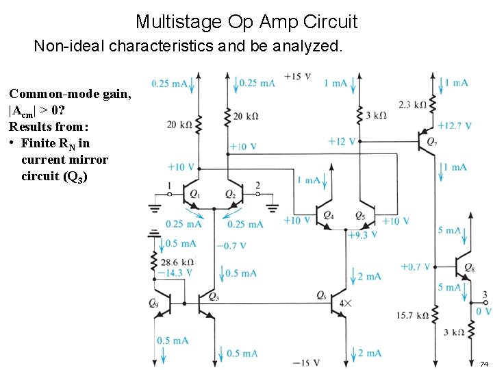
Multistage Op Amp Circuit Non-ideal characteristics and be analyzed. Common-mode gain, |Acm| > 0? 73

Multistage Op Amp Circuit Non-ideal characteristics and be analyzed. Common-mode gain, |Acm| > 0? Results from: • Finite RN in current mirror circuit (Q 3) 74

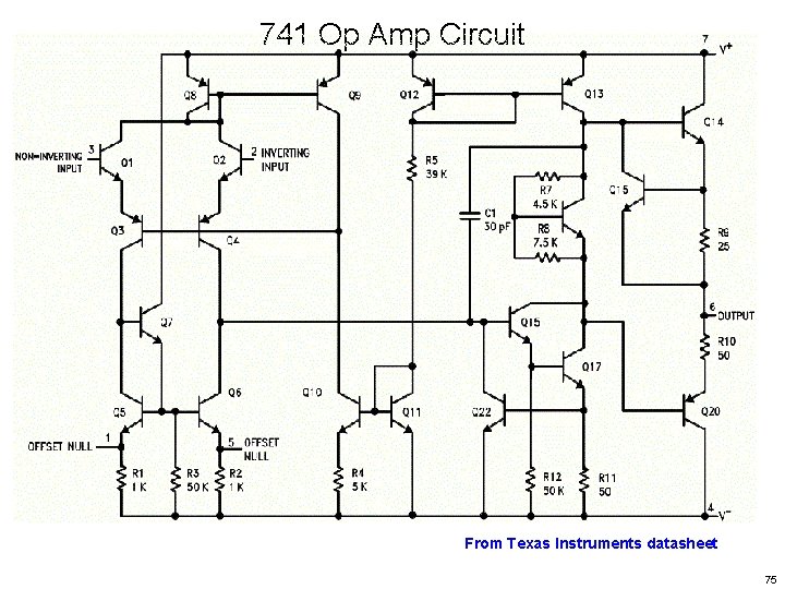
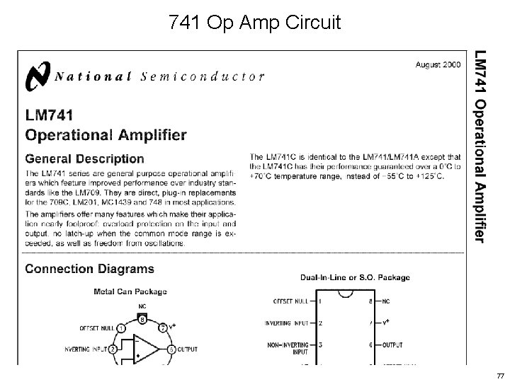
741 Op Amp Circuit From Texas Instruments datasheet 75

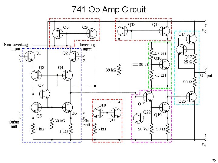
741 Op Amp Circuit 76

741 Op Amp Circuit 77

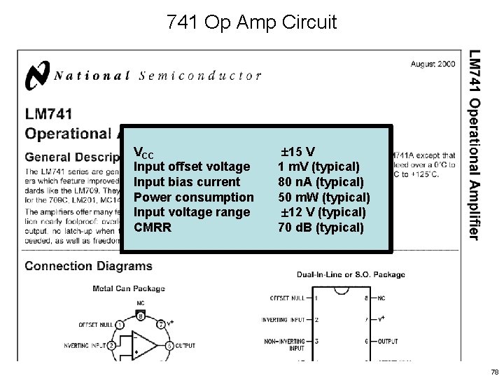
741 Op Amp Circuit VCC Input offset voltage Input bias current Power consumption Input voltage range CMRR 15 V 1 m. V (typical) 80 n. A (typical) 50 m. W (typical) 12 V (typical) 70 d. B (typical) 78