Small Signal Model MOS FieldEffect Transistors MOSFETs 1
 1")
 20 -03 -07 Rout. (a) (b) (c) Draw")


 : Configuration")
 • Most widely used • Signal ground or an ac")
")
")

 Summary • Input Resistance is infinite (Ri=∞) • Output Resistance")


 Amplifier • The input signal is applied to the source •")


 A common-drain or source-follower amplifier : output resistance Rout of the source follower.")
 A common-drain or source-follower amplifier. : Smallsignal analysis performed directly on the circuit.")
")
 With RS")
 Current Follower")
 Source Follower")


 Rout")


")
")


 Replacing BJT with MOSFET")


")
 + vbe 2 + veb 1 -")
 + vbe 2 + veb 1 + vi -")
 with MOSFET")
 + vgs 2 + vsg 1 -")
 + vgs 2 + vsg 1 ig 1=0 + vi")


=2 m. A/V 2 Vt=1 V")

=2 m. A/V 2 Vt 1=1 V Vt 2=25")


- Slides: 100
Small Signal Model MOS Field-Effect Transistors (MOSFETs) 1
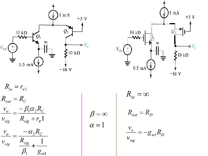
Quiz No 3 DE 27 (CE) 20 -03 -07 Rout. (a) (b) (c) Draw small signal model (4) Find expression for Rout (2) Prove vo/vsig = (β 1α 2 RC)/(Rsig+rπ) (4).
Figure 4. 2 The enhancement-type NMOS transistor with a positive voltage applied to the gate. An n channel is induced at the top of the substrate beneath the gate.
Enhancement-type NMOS transistor:
MOSFET Analysis i. D = i. S, i. G = 0
Large-signal equivalent-circuit model of an n-channel MOSFET : Operating in the saturation region.
Large-signal equivalent-circuit model of an p-channel MOSFET : Operating in the saturation region.
Large Signal Model : MOSFET
Transfer characteristic of an amplifier
Conceptual circuit utilized to study the operation of the MOSFET as a small-signal amplifier. The DC BIAS POINT To Ensure Saturation-region Operation
Signal Current in Drain Terminal
Total instantaneous voltages v. GS and v. D
Small-signal ‘π’ models for the MOSF
Common Source amplifier circuit Example 4 -10
Small Signal ‘T’ Model : NMOSFET
Small Signal Models ‘T’ Model
Single Stage MOS Amplifier
Amplifiers Configurations
Common Source Amplifier (CS) : Configuration
Common Source Amplifier (CS) • Most widely used • Signal ground or an ac earth is at the source through a bypass capacitor • Not to disturb dc bias current & voltages coupling capacitors are used to pass the signal voltages to the input terminal of the amplifier or to the Load Resistance • CS circuit is unilateral – – Rin does not depend on RL and vice versa
Small Signal Hybrid “π” Model (CS)
Small Signal Hybrid “π” Model : (CS)
Small-signal analysis performed directly on the amplifier circuit with the MOSFET model implicitly utilized.
Common Source Amplifier (CS) Summary • Input Resistance is infinite (Ri=∞) • Output Resistance = RD • Voltage Gain is substantial
Common-source amplifier with a resistance RS in the source lead
The Common Source Amplifier with a Source Resistance • The ‘T’ Model is preferred, whenever a resistance is connected to the source terminal. • ro (output resistance due to Early Effect) is not included, as it would make the amplifier non unilateral & effect of using ro in model would be studied in Chapter ‘ 6’
Small-signal equivalent circuit with ro neglected.
Small-signal Analysis.
Voltage Gain : CS with RS
Common Source Configuration with Rs • Rs causes a negative feedback thus improving the stability of drain current of the circuit but at the cost of voltage gain • Rs reduces id by the factor – (1+gm. Rs) = Amount of feedback • Rs is called Source degeneration resistance as it reduces the gain
Small-signal equivalent circuit directly on Circuit
A common-gate amplifier based on the circuit
Common Gate (CG) Amplifier • The input signal is applied to the source • Output is taken from the drain • The gate is formed as a common input & output port. • ‘T’ Model is more Convenient • ro is neglected
A small-signal equivalent circuit
A small-signal Analusis : CG
A small-signal Analusis : CG
Small signal analysis directly on circuit
The common-gate amplifier fed with a current-signal input.
Summary : CG 4. CG has much higher output Resistance 5. CG is unity current Gain amplifier or a Current Buffer 6. CG has superior High Frequency Response.
A common-drain or source-follower amplifier.
Small-signal equivalent-circuit model
Small-signal Analysis : CD
(a) A common-drain or source-follower amplifier : output resistance Rout of the source follower.
(a) A common-drain or source-follower amplifier. : Smallsignal analysis performed directly on the circuit.
Common Source Circuit (CS)
Common Source Circuit (CS) With RS
Common Gate Circuit (CG) Current Follower
Common Drain Circuit (CD) Source Follower
Summary & Comparison
Quiz No 4 • Draw/Write the Following: Types Symbols ‘π’ Model T Model gm Re/rs rπ/rg BJT npn pnp MOSFET n. MOS p. MOS 27 -03 -07
Problem 5 -44
SOLUTION : DC Analysis
SOLUTION : DC Analysis IE IB Check for Active Mode
Solution Small Signal Analysis
Solution Small Signal Analysis
Solution Small Signal Analysis : Input Resistance ib + vb - Rin
Solution Small Signal Analysis : Output Resistance Itest IE IRC IE/(1+ß) Rout
Solution Small Signal Analysis : Voltage Gain + veb - - + Vo vi + -
Solution Small Signal Analysis : Voltage gain + veb + vi -
Solution Small Signal Analysis : Voltage Gain + vi -
Solution Small Signal Analysis : Voltage Gain
Solution Small Signal Analysis : Voltage Gain + vi - Vo +
Problem
Small Signal Model MOSFET : CD
Solution Small Signal Analysis 1/gm D gmvsg
Solution Small Signal Analysis : Input Resistance 1/gm Ig=0 D gmvsg Rin
Solution Small Signal Analysis : Output Resistance Itest 1/gm ID IG=0 IRD D gmvsg Rout Vtest
Solution Small Signal Analysis : Voltage Gain + vsg 1/gm - - + vi - gmvsg D +
Solution Small Signal Analysis : Voltage gain + vsg 1/gm + vi - D gmvsg
Solution Small Signal Analysis : Voltage Gain + vi -
Solution Small Signal Analysis : Voltage Gain
Solution Small Signal Analysis : Voltage Gain + vi - +
Solution Small Signal Analysis
Problem 6 -127(e)
DC Analysis 6 -127(e)
Small Signal Model
Small Signal Model
Small Signal Model Rin Rout
Problem 6 -127(f) Replacing BJT with MOSFET
Small Signal Model
Small Signal Model
Small Signal Model Rin Rout
Problem 6 -127(f)
Solution P 6 -127(f) + vbe 2 + veb 1 -
Solution P 6 -127(f) + vbe 2 + veb 1 + vi -
Problem 6 -127(f) with MOSFET
Solution P 6 -127(f) + vgs 2 + vsg 1 -
Solution P 6 -127(f) + vgs 2 + vsg 1 ig 1=0 + vi -
Comparison BJT/MOSFET Cct
Small Signal Model
Problem 6 -123 VBE=0. 7 V β =200 K’n(W/L)=2 m. A/V 2 Vt=1 V Figure P 6. 123
DC Analysis Figure P 6. 123
VBE=0. 7 V β =200 K’n(W/L)=2 m. A/V 2 Vt 1=1 V Vt 2=25 m. V DC Analysis 1 m. A 2 V IG 0. 7 V =0 I=0. 7/6. 8=0. 1 m. A
Small Signal Model
Small Signal Model
Small Signal Model : Voltage Gain + ig=0 vi - + vbe 2 -
Small Signal Model : Input Resistance ii + ig=0 vi Rin