SLP 1 design Christos Gentsos 942014 SLP 1
- Slides: 11

SLP 1 design Christos Gentsos 9/4/2014

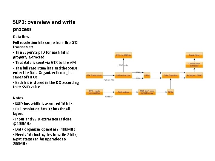
SLP 1: overview and write process Data flow Full resolution hits come from the GTX transceivers • The Super. Strip ID for each hit is properly extracted • That data is send via GTX to the AM • The full resolution hits and the SSIDs enter the Data Organizer through a series of FIFOs • Each hit is stored in the DO according to its SSID value Notes • SSID bus width is assumed 16 bits • Full resolution hits 32 bits for all layers • Input and SSID extraction is done @100 MHz • Data organizer operates @400 MHz • Needs 16 clock cycles to write 8 hits, input stage can be upgraded to 200 MHz

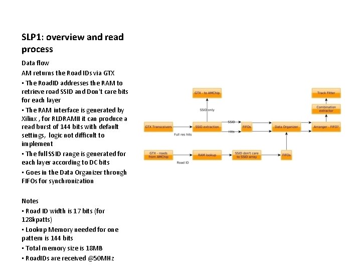
SLP 1: overview and read process Data flow AM returns the Road IDs via GTX • The Road. ID addresses the RAM to retrieve road SSID and Don't care bits for each layer • The RAM interface is generated by Xilinx , for RLDRAMII it can produce a read burst of 144 bits with default settings, logic not difficult to implement • The full SSID range is generated for each layer according to DC bits • Goes in the Data Organizer through FIFOs for synchronization Notes • Road ID width is 17 bits (for 128 kpatts) • Lookup Memory needed for one pattern is 144 bits • Total memory size is 18 MB • Road. IDs are received @50 MHz

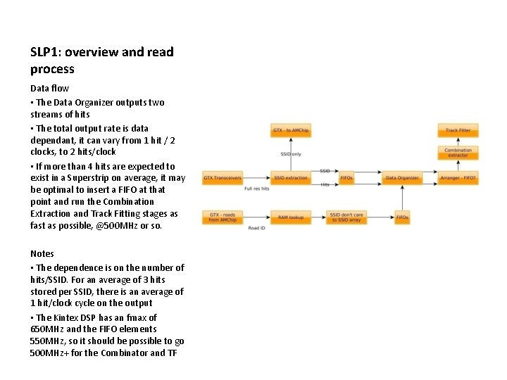
SLP 1: overview and read process Data flow • The Data Organizer outputs two streams of hits • The total output rate is data dependant, it can vary from 1 hit / 2 clocks, to 2 hits/clock • If more than 4 hits are expected to exist in a Superstrip on average, it may be optimal to insert a FIFO at that point and run the Combination Extraction and Track Fitting stages as fast as possible, @500 MHz or so. Notes • The dependence is on the number of hits/SSID. For an average of 3 hits stored per SSID, there is an average of 1 hit/clock cycle on the output • The Kintex DSP has an fmax of 650 MHz and the FIFO elements 550 MHz, so it should be possible to go 500 MHz+ for the Combinator and TF

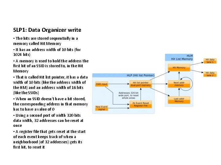
SLP 1: Data Organizer write • The hits are stored sequentially in a memory called Hit Memory • It has an address width of 10 bits (for 1024 hits) • A memory is used to hold the address the first hit of an SSID is stored to, in the Hit Memory • That is called Hit list pointer, it has a data width of 10 bits (like the address width of the HM) and an address width of 16 bits (like the SSIDs) • When an SSID doesn't have a hit stored, the corresponding address in that memory has to have a value of 0 • Using a second port of width 320 bits data width, 32 addresses can be reset at once • A register file that gets reset at the start of each event keeps track of when a neighborhood (of 32 addresses) gets its first hit, to reset it

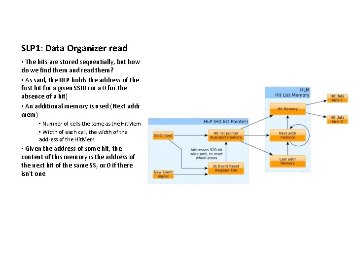
SLP 1: Data Organizer read • The hits are stored sequentially, but how do we find them and read them? • As said, the HLP holds the address of the first hit for a given SSID (or a 0 for the absence of a hit) • An additional memory is used (Next addr mem) • Number of cells the same as the Hit. Mem • Width of each cell, the width of the address of the Hit. Mem • Given the address of some hit, the content of this memory is the address of the next hit of the same SS, or 0 if there isn't one

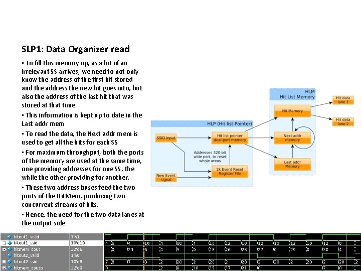
SLP 1: Data Organizer read • To fill this memory up, as a hit of an irrelevant SS arrives, we need to not only know the address of the first hit stored and the address the new hit goes into, but also the address of the last hit that was stored at that time • This information is kept up to date in the Last addr mem • To read the data, the Next addr mem is used to get all the hits for each SS • For maximum throughput, both the ports of the memory are used at the same time, one providing addresses for one SS, the while the other providing for another. • These two address buses feed the two ports of the Hit. Mem, producing two concurrent streams of hits. • Hence, the need for the two data lanes at the output side

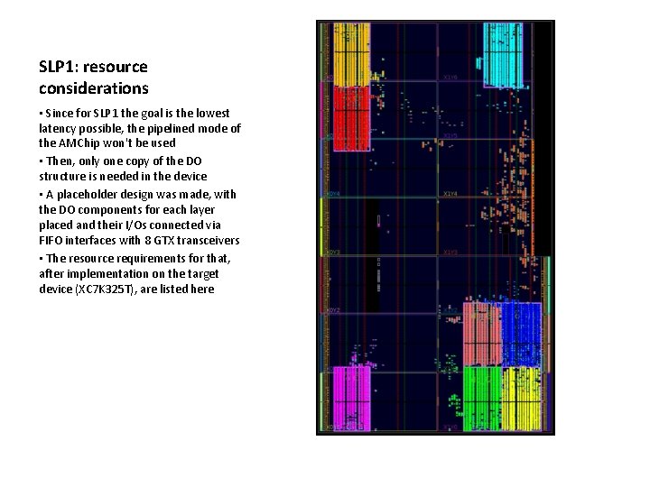
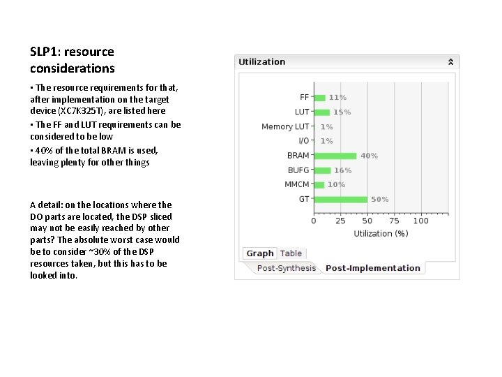
SLP 1: resource considerations • Since for SLP 1 the goal is the lowest latency possible, the pipelined mode of the AMChip won't be used • Then, only one copy of the DO structure is needed in the device • A placeholder design was made, with the DO components for each layer placed and their I/Os connected via FIFO interfaces with 8 GTX transceivers • The resource requirements for that, after implementation on the target device (XC 7 K 325 T), are listed here

SLP 1: resource considerations • The resource requirements for that, after implementation on the target device (XC 7 K 325 T), are listed here • The FF and LUT requirements can be considered to be low • 40% of the total BRAM is used, leaving plenty for other things A detail: on the locations where the DO parts are located, the DSP sliced may not be easily reached by other parts? The absolute worst case would be to consider ~30% of the DSP resources taken, but this has to be looked into.

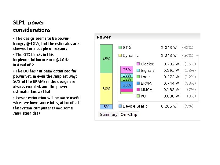
SLP 1: power considerations • The design seems to be powerhungry @4. 5 W, but the estimates are skewed for a couple of reasons • The GTX blocks in this implementation are run @4 GHz instead of 2 • The DO has not been optimized for power yet, in even the simplest way: 90% of the BRAMs in the design are always enabled, and the power estimator knows that • Power estimation will be more useful when we have some integration of all the system components and some simulation data

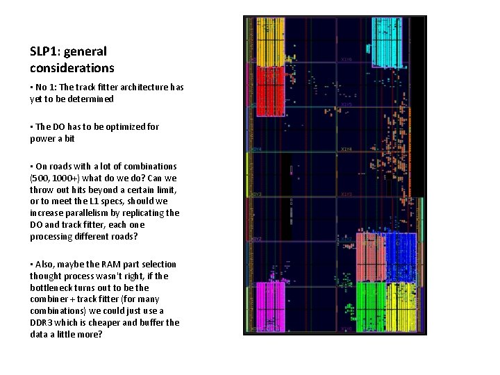
SLP 1: general considerations • No 1: The track fitter architecture has yet to be determined • The DO has to be optimized for power a bit • On roads with a lot of combinations (500, 1000+) what do we do? Can we throw out hits beyond a certain limit, or to meet the L 1 specs, should we increase parallelism by replicating the DO and track fitter, each one processing different roads? • Also, maybe the RAM part selection thought process wasn't right, if the bottleneck turns out to be the combiner + track fitter (for many combinations) we could just use a DDR 3 which is cheaper and buffer the data a little more?