SKIROC 2CMS for the CMS HGCAL Ludovic Raux
- Slides: 28

SKIROC 2–CMS for the CMS HGCAL Ludovic Raux June 1 st, 2016 Organization for Micro-Electronics desi. Gn and Applications

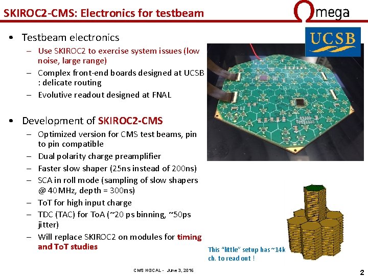
SKIROC 2 -CMS: Electronics for testbeam • Testbeam electronics – Use SKIROC 2 to exercise system issues (low noise, large range) – Complex front-end boards designed at UCSB : delicate routing – Evolutive readout designed at FNAL • Development of SKIROC 2 -CMS – Optimized version for CMS test beams, pin to pin compatible – Dual polarity charge preamplifier – Faster slow shaper (25 ns instead of 200 ns) – SCA in roll mode (sampling of slow shapers @ 40 MHz, depth = 300 ns) – To. T for high input charge – TDC (TAC) for To. A (~20 ps binning, ~50 ps jitter) – Will replace SKIROC 2 on modules for timing and To. T studies CMS HGCAL - June 3, 2016 This “little” setup has ~14 k ch. to read out ! 2

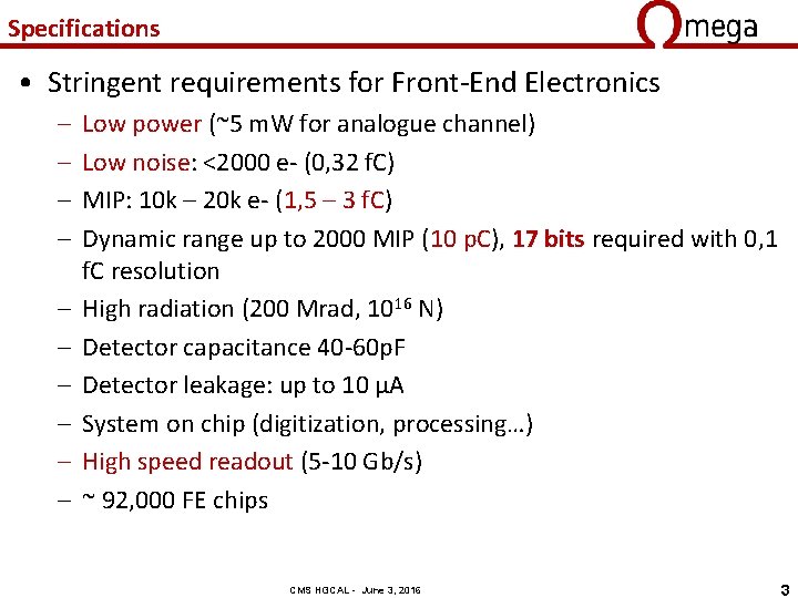
Specifications • Stringent requirements for Front-End Electronics – – – – – Low power (~5 m. W for analogue channel) Low noise: <2000 e- (0, 32 f. C) MIP: 10 k – 20 k e- (1, 5 – 3 f. C) Dynamic range up to 2000 MIP (10 p. C), 17 bits required with 0, 1 f. C resolution High radiation (200 Mrad, 1016 N) Detector capacitance 40 -60 p. F Detector leakage: up to 10 µA System on chip (digitization, processing…) High speed readout (5 -10 Gb/s) ~ 92, 000 FE chips CMS HGCAL - June 3, 2016 3

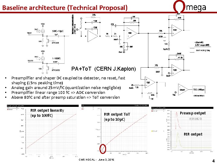
Baseline architecture (Technical Proposal) PA+To. T (CERN J. Kaplon) • • Preamplifier and shaper DC coupled to detector, no reset, fast shaping (15 ns peaking time) Analog gain around 25 m. V/f. C (quantization noise negligible) Preamplifier linear range 100 f. C => ADC conversion Above 80 f. C and after preamp saturation => To. T conversion Rt. R output linearity (up to 100 f. C) Rt. R output To. T (up to 10 p. C) Preamp output Rt. R output CMS HGCAL - June 3, 2016 4

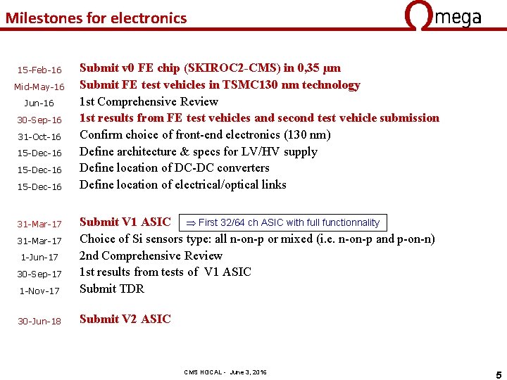
Milestones for electronics 15 -Feb-16 Mid-May-16 Jun-16 30 -Sep-16 31 -Oct-16 15 -Dec-16 Submit v 0 FE chip (SKIROC 2 -CMS) in 0, 35 µm Submit FE test vehicles in TSMC 130 nm technology 1 st Comprehensive Review 1 st results from FE test vehicles and second test vehicle submission Confirm choice of front-end electronics (130 nm) Define architecture & specs for LV/HV supply Define location of DC-DC converters Define location of electrical/optical links 1 -Nov-17 Submit V 1 ASIC First 32/64 ch ASIC with full functionnality Choice of Si sensors type: all n-on-p or mixed (i. e. n-on-p and p-on-n) 2 nd Comprehensive Review 1 st results from tests of V 1 ASIC Submit TDR 30 -Jun-18 Submit V 2 ASIC 31 -Mar-17 1 -Jun-17 30 -Sep-17 CMS HGCAL - June 3, 2016 5

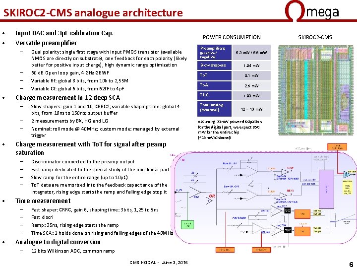
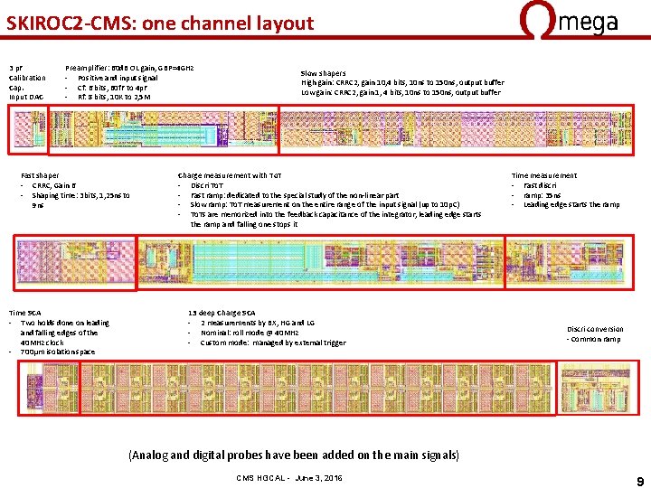
SKIROC 2 -CMS analogue architecture • • Input DAC and 3 p. F calibration Cap. Versatile preamplifier – – • – – Preamplifiers (positive / negative) 5, 3 m. W / 5, 6 m. W Slow shapers 1, 94 m. W To. T 0, 1 m. W To. A 2, 6 m. W TDC 1, 93 m. W Total analog (/channel) SKIROC 2 -CMS 12 – 13 m. W Assuming 20 m. W power dissipation for the digital part, we expect 850 m. W for the entire chip (<15 m. W/channel) Discriminator connected to the preamp output Fast ramp dedicated to the special study of the non-linear part Slow ramp for the entire range (up to 10 p. C) To. T data are memorized into the feedback capacitance of the integrator, rising edge starts the ramp and falling edge stop it Time measurement – – • Slow shapers: gain 1 and 10, CRRC 2; variable shaping time: global 4 bits, from 10 ns to 150 ns; output buffer 2 measurements by BX, HG and LG Nominal: roll mode @ 40 MHz; custom mode: managed by external trigger Charge measurement with To. T for signal after peamp saturation – – • Dual polarity: single first stage with input PMOS transistor (available NMOS are directly on substrate), one feedback for each polarity (likely better for positive input charge), high dynamic range optimization 60 d. B Open loop gain, 4 GHz GBWP Variable Rf: global 8 bits, from 10 k to 2, 55 M Variable Cf: global 6 bits, from 62 f. F to 4 p. F Charge measurement in 12 deep SCA – • POWER CONSUMPTION Fast shaper: CRRC, gain 6, shaping time: 3 bits, 1, 25 to 9 ns Fast discri Ramp: 35 ns, rising edge starts the ramp Time SCA: 2 holds done on rising and falling edges of the 40 MHz Analogue to digital conversion – 12 bits Wilkinson ADC, common ramp CMS HGCAL - June 3, 2016 6

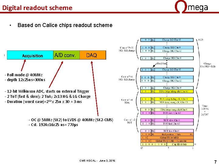
Digital readout scheme • Based on Calice chips readout scheme - Roll mode @ 40 MHz - depth 12 x 25 ns=300 ns - 12 -bit Wilkinson ADC, starts on external Trigger - 2 To. T (fast & slow); 2 To. A; 2 x 13 HG & LG Charge - Duration (worst case)=212 x 25 n x 30 = 3 ms - OC @ 5 MHz (SK 2) to LVDS @ 40 MHz (SK 2 -CMS) - Cst. 1924 x 16 x 25 ns= 770µs CMS HGCAL - June 3, 2016 7

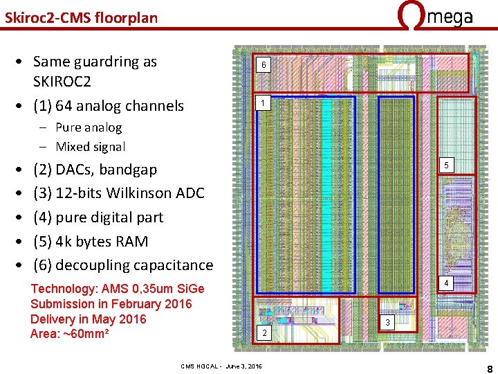
Skiroc 2 -CMS floorplan • Same guardring as SKIROC 2 • (1) 64 analog channels 6 1 – Pure analog – Mixed signal • • • (2) DACs, bandgap (3) 12 -bits Wilkinson ADC (4) pure digital part (5) 4 k bytes RAM (6) decoupling capacitance Technology: AMS 0, 35 um Si. Ge Submission in February 2016 Delivery in May 2016 Area: ~60 mm² 5 4 3 2 CMS HGCAL - June 3, 2016 8

SKIROC 2 -CMS: one channel layout 3 p. F Calibration Cap. Input DAC Preamplifier: 60 d. B OL gain, GBP=4 GHz - Positive and input signal - Cf: 6 bits, 60 f. F to 4 p. F - Rf: 8 bits, 10 K to 2, 5 M Fast shaper - CRRC, Gain 6 - Shaping time: 3 bits, 1, 25 ns to 9 ns Time SCA - Two holds done on leading and falling edges of the 40 MHz clock - 700μm isolation space Slow shapers High gain: CRRC 2, gain 10, 4 bits, 10 ns to 150 ns, output buffer Low gain: CRRC 2, gain 1, 4 bits, 10 ns to 150 ns, output buffer Charge measurement with To. T - Discri To. T - Fast ramp: dedicated to the special study of the non-linear part - Slow ramp: To. T measurement on the entire range of the input signal (up to 10 p. C) - To. Ts are memorized into the feedback capacitance of the integrator, leading edge starts the ramp and falling one stops it 13 deep Charge SCA - 2 measurements by BX, HG and LG - Nominal: roll mode @ 40 MHz - Custom mode: managed by external trigger Time measurement - Fast discri - ramp: 35 ns - Leading edge starts the ramp Discri conversion - Common ramp (Analog and digital probes have been added on the main signals) CMS HGCAL - June 3, 2016 9

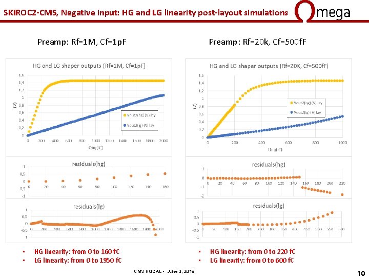
SKIROC 2 -CMS, Negative input: HG and LG linearity post-layout simulations Preamp: Rf=1 M, Cf=1 p. F • • Preamp: Rf=20 k, Cf=500 f. F HG linearity: from 0 to 160 f. C LG linearity: from 0 to 1950 f. C • • CMS HGCAL - June 3, 2016 HG linearity: from 0 to 220 f. C LG linearity: from 0 to 600 f. C 10

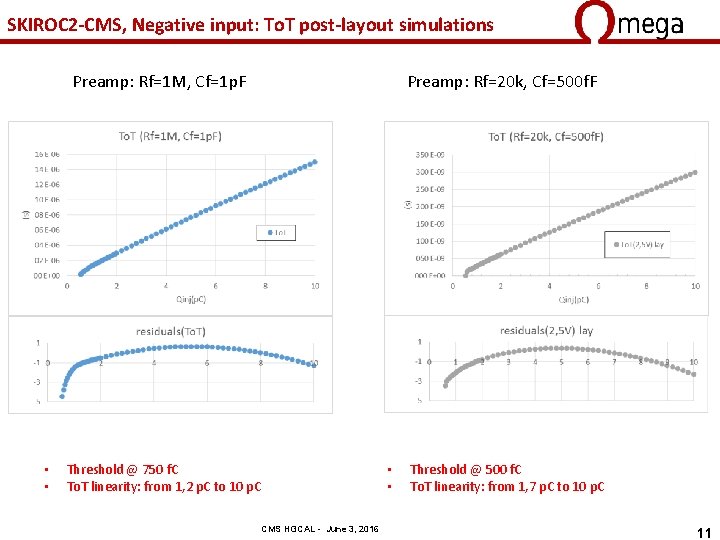
SKIROC 2 -CMS, Negative input: To. T post-layout simulations Preamp: Rf=1 M, Cf=1 p. F • • Preamp: Rf=20 k, Cf=500 f. F Threshold @ 750 f. C To. T linearity: from 1, 2 p. C to 10 p. C CMS HGCAL - June 3, 2016 • • Threshold @ 500 f. C To. T linearity: from 1, 7 p. C to 10 p. C 11

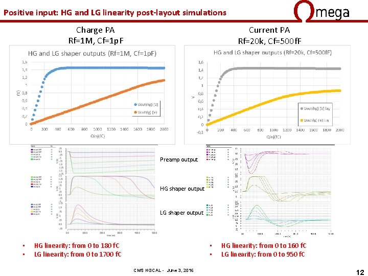
Positive input: HG and LG linearity post-layout simulations Charge PA Rf=1 M, Cf=1 p. F Current PA Rf=20 k, Cf=500 f. F Preamp output HG shaper output LG shaper output • • HG linearity: from 0 to 180 f. C LG linearity: from 0 to 1700 f. C • • CMS HGCAL - June 3, 2016 HG linearity: from 0 to 160 f. C LG linearity: from 0 to 950 f. C 12

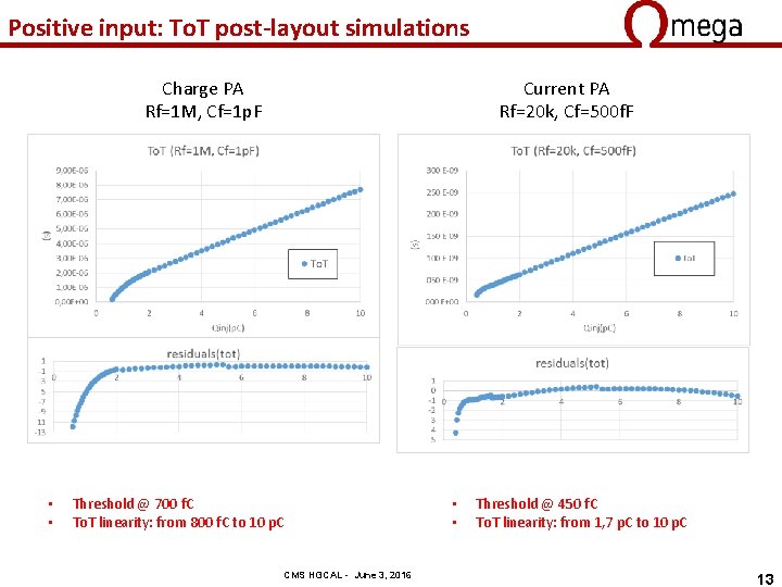
Positive input: To. T post-layout simulations Charge PA Rf=1 M, Cf=1 p. F • • Current PA Rf=20 k, Cf=500 f. F Threshold @ 700 f. C To. T linearity: from 800 f. C to 10 p. C CMS HGCAL - June 3, 2016 • • Threshold @ 450 f. C To. T linearity: from 1, 7 p. C to 10 p. C 13

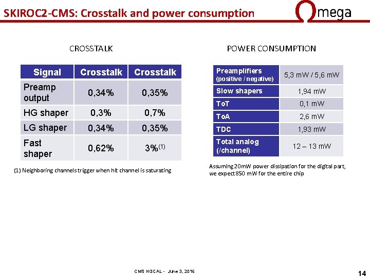
SKIROC 2 -CMS: Crosstalk and power consumption CROSSTALK Signal POWER CONSUMPTION Crosstalk Preamplifiers Preamp output 0, 34% 0, 35% Slow shapers 1, 94 m. W HG shaper To. T 0, 3% 0, 7% 0, 1 m. W To. A 2, 6 m. W LG shaper 0, 34% 0, 35% TDC 1, 93 m. W Fast shaper 0, 62% 3%(1) Neighboring channels trigger when hit channel is saturating CMS HGCAL - June 3, 2016 (positive / negative) Total analog (/channel) 5, 3 m. W / 5, 6 m. W 12 – 13 m. W Assuming 20 m. W power dissipation for the digital part, we expect 850 m. W for the entire chip 14

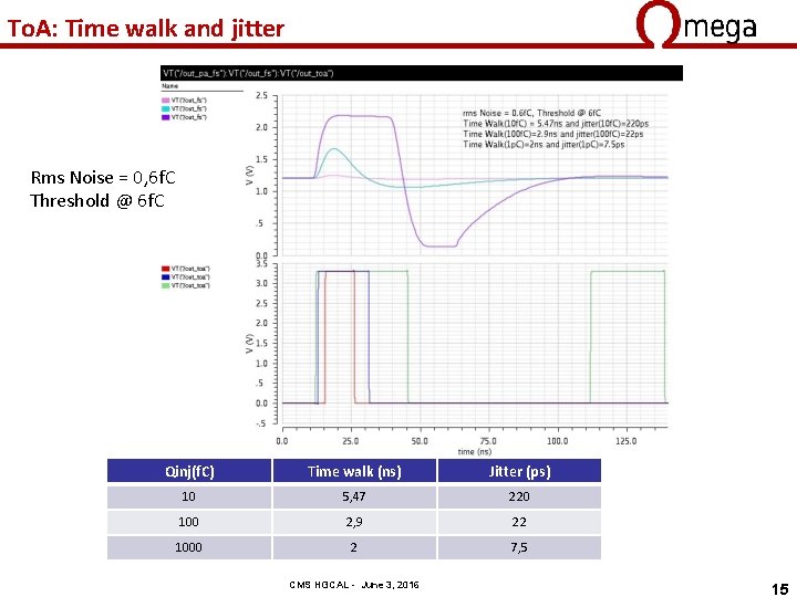
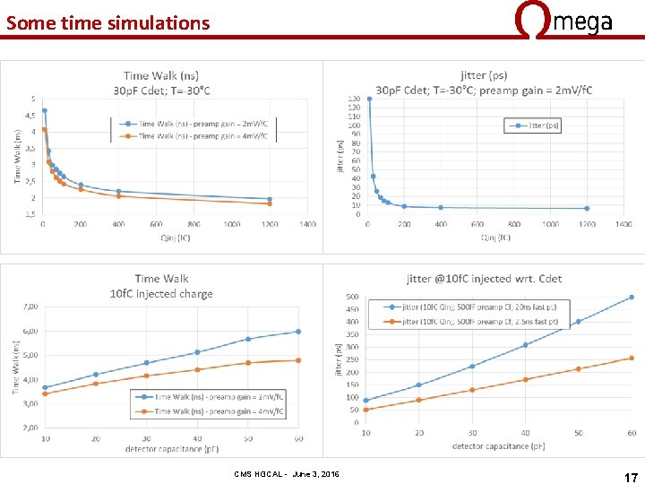
To. A: Time walk and jitter Rms Noise = 0, 6 f. C Threshold @ 6 f. C Qinj(f. C) Time walk (ns) Jitter (ps) 10 5, 47 220 100 2, 9 22 1000 2 7, 5 CMS HGCAL - June 3, 2016 15

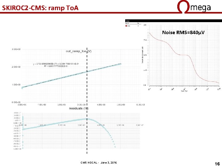
SKIROC 2 -CMS: ramp To. A Noise RMS=840µV CMS HGCAL - June 3, 2016 16

Some time simulations CMS HGCAL - June 3, 2016 17

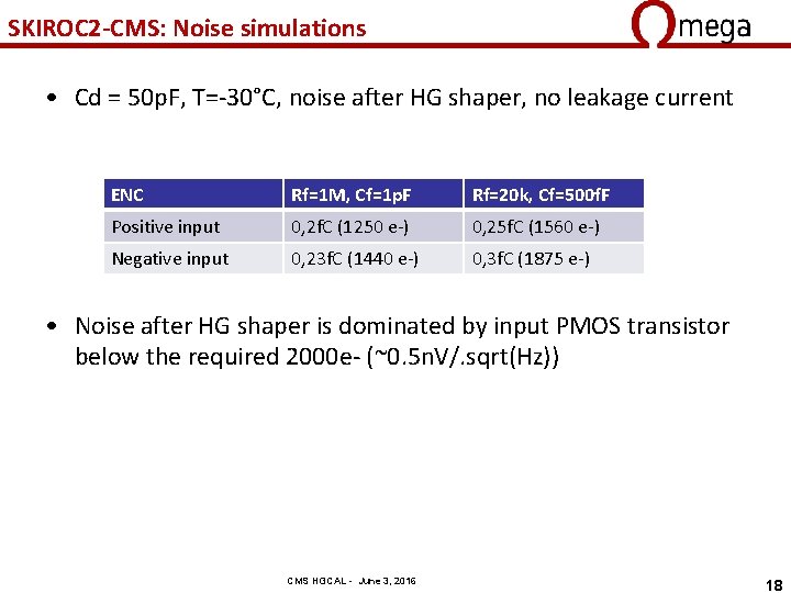
SKIROC 2 -CMS: Noise simulations • Cd = 50 p. F, T=-30°C, noise after HG shaper, no leakage current ENC Rf=1 M, Cf=1 p. F Rf=20 k, Cf=500 f. F Positive input 0, 2 f. C (1250 e-) 0, 25 f. C (1560 e-) Negative input 0, 23 f. C (1440 e-) 0, 3 f. C (1875 e-) • Noise after HG shaper is dominated by input PMOS transistor below the required 2000 e- (~0. 5 n. V/. sqrt(Hz)) CMS HGCAL - June 3, 2016 18

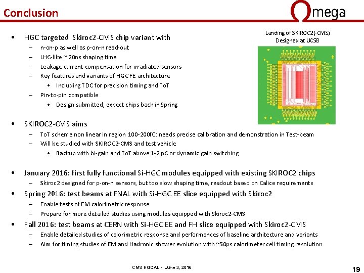
Conclusion • HGC targeted Skiroc 2 -CMS chip variant with – – – • SKIROC 2 -CMS aims – – • Skiroc 2 designed for p-on-n sensors, but too slow shaping time, readout based on Calice requirements Spring 2016: test beams at FNAL with Si-HGC EE slice equipped with Skiroc 2 – – • To. T scheme non linear in region 100 -200 f. C: needs precise calibration and demonstration in Test-beam Will be studied with SKIROC 2 -CMS and test vehicle • Backup with bi-gain and To. T above 1 -2 p. C or dynamic gain switching January 2016: first fully functional Si-HGC modules equipped with existing SKIROC 2 chips – • n-on-p as well as p-on-n read-out LHC-like ~ 20 ns shaping time Leakage current compensation for irradiated sensors Key features and variants of HGC FE architecture • Including TDC for precision timing and To. T Pin-to-pin compatible • Design submitted, expect chips back in Spring Landing of SKIROC 2(-CMS) Designed at UCSB Enable tests of EM calorimetric response Prepare for more detailed studies using modules equipped with Skiroc 2 -CMS Fall 2016: test beams at CERN with Si-HGC EE and FH slice equipped with Skiroc 2 -CMS – – Enable detailed studies of calorimetric response and performances of baseline architecture and variants Aim for timing studies of EM and Hadronic shower evolution with ~50 ps calorimeter cell timing resolution CMS HGCAL - June 3, 2016 19

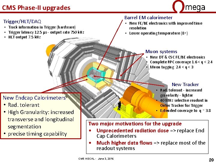
CMS Phase-II upgrades Barrel EM calorimeter Trigger/HLT/DAQ • New FE/BE electronics with improved time resolution • Lower operating temperature (8∘) • Track information in Trigger (hardware) • Trigger latency 12. 5 µs - output rate 750 k. Hz • HLT output 7. 5 k. Hz Muon systems • New DT & CSC FE/BE electronics • Complete RPC coverage 1. 6 < η < 2. 4 • Muon tagging 2. 4 < η < 3 New Tracker New Endcap Calorimeters • Rad. tolerant • High Granularity: increased transverse and longitudinal segmentation • precise timing capability • Rad. tolerant - increased granularity - lighter • 40 MHz selective readout in Outer Tracker for Trigger • Extended coverage to η ≃ 3. 8 Two major motivations for the upgrade • Unprecedented radiation dose => replace End Cap Calorimeters • Much higher data flows => replace most of the readout systems CMS HGCAL - June 3, 2016 20

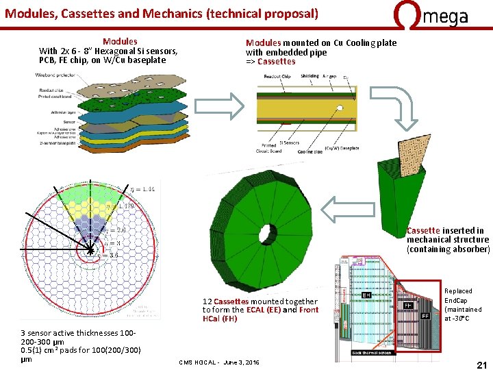
Modules, Cassettes and Mechanics (technical proposal) Modules With 2 x 6 - 8” Hexagonal Si sensors, PCB, FE chip, on W/Cu baseplate Modules mounted on Cu Cooling plate with embedded pipe => Cassettes Cassette inserted in mechanical structure (containing absorber) 12 Cassettes mounted together to form the ECAL (EE) and Front HCal (FH) 3 sensor active thicknesses 100200 -300 µm 0. 5(1) cm 2 pads for 100(200/300) µm CMS HGCAL - June 3, 2016 Replaced End. Cap (maintained at -30°C 21

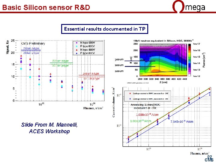
Basic Silicon sensor R&D Essential results documented in TP 300 um 200 um 100 um Slide From M. Mannelli, ACES Workshop 22 CMS

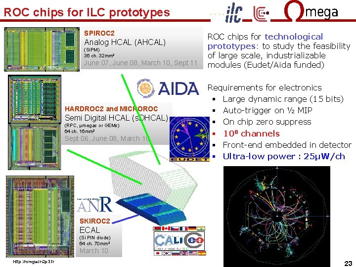
ROC chips for ILC prototypes SPIROC 2 q ROC chips for technological prototypes: to study the feasibility (Si. PM) 36 ch. 32 mm² of large scale, industrializable June 07, June 08, March 10, Sept 11 modules (Eudet/Aida funded) Analog HCAL (AHCAL) HARDROC 2 and MICROROC Semi Digital HCAL (s. DHCAL) (RPC, µmegas or GEMs) 64 ch. 16 mm² Sept 06, June 08, March 10 q Requirements for electronics § Large dynamic range (15 bits) § Auto-trigger on ½ MIP § On chip zero suppress § 108 channels § Front-end embedded in detector § Ultra-low power : 25µW/ch SKIROC 2 ECAL (Si PIN diode) 64 ch. 70 mm² March 10 http: //omga. in 2 p 3. fr 23

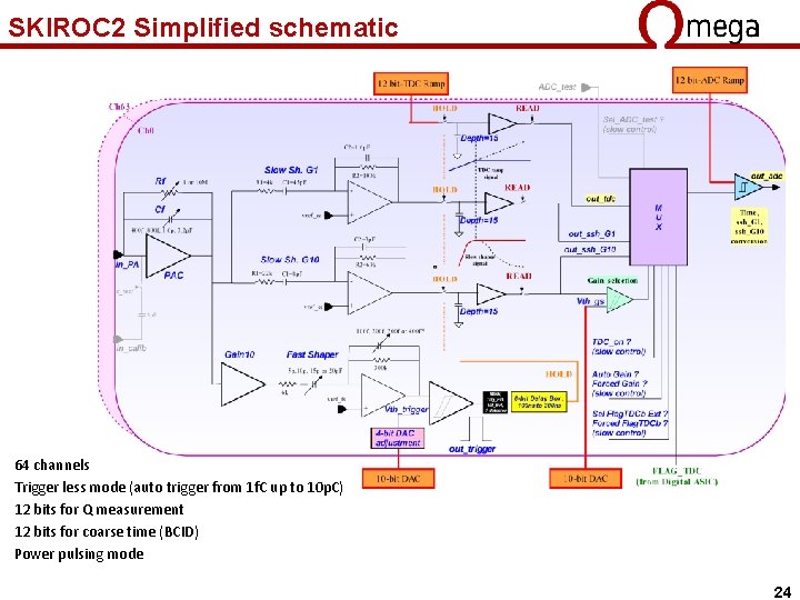
SKIROC 2 Simplified schematic 64 channels Trigger less mode (auto trigger from 1 f. C up to 10 p. C) 12 bits for Q measurement 12 bits for coarse time (BCID) Power pulsing mode 24

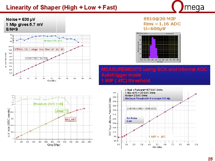
Linearity of Shaper (High + Low + Fast) SS 10@20 MIP Rms =1. 16 ADC U=600µV Noise = 630 µV 1 Mip gives 5. 7 m. V S/N=9 MEASUREMENTS using SCA and internal ADC Autotrigger mode 1 MIP ( 4 f. C) threshold « Real » Pedestal=167 DAC Units 1 Mip ≈4 f. C = 20 DAC Units Noise= 2 DAC Units Minimum Threshold= 5 σ noise= 0. 5 Mip 5σ Noise limit 1 MIP ≈ 4 f. C 25

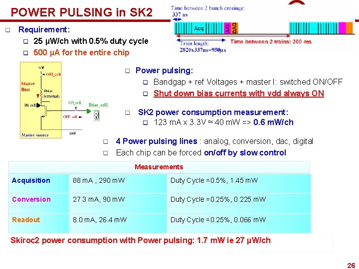
POWER PULSING in SK 2 q Requirement: q 25 µW/ch with 0. 5% duty cycle q 500 µA for the entire chip q q Power pulsing: q Bandgap + ref Voltages + master I: switched ON/OFF q Shut down bias currents with vdd always ON SK 2 power consumption measurement: q 123 m. A x 3. 3 V ≈ 40 m. W => 0. 6 m. W/ch 4 Power pulsing lines : analog, conversion, dac, digital Each chip can be forced on/off by slow control Measurements Acquisition 88 m. A , 290 m. W Duty Cycle =0. 5%, 1. 45 m. W Conversion 27. 3 m. A, 90 m. W Duty Cycle =0. 25%, 0. 225 m. W Readout 8. 0 m. A, 26. 4 m. W Duty Cycle =0. 25%, 0. 066 m. W Skiroc 2 power consumption with Power pulsing: 1. 7 m. W ie 27 µW/ch 26

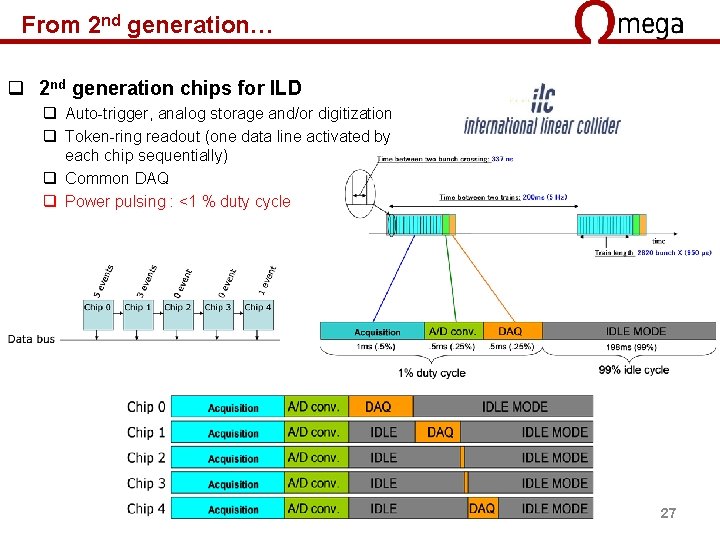
From 2 nd generation… q 2 nd generation chips for ILD q Auto-trigger, analog storage and/or digitization q Token-ring readout (one data line activated by each chip sequentially) q Common DAQ q Power pulsing : <1 % duty cycle 27

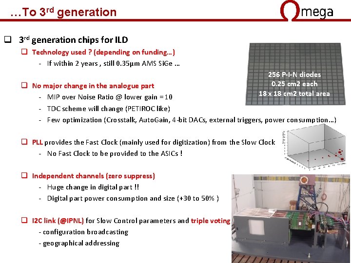
…To 3 rd generation q 3 rd generation chips for ILD q Technology used ? (depending on funding…) - If within 2 years , still 0. 35µm AMS Si. Ge … 256 P-I-N diodes 0. 25 cm 2 each 18 x 18 cm 2 total area q No major change in the analogue part - MIP over Noise Ratio @ lower gain = 10 - TDC scheme will change (PETIROC like) - Few optimization (Crosstalk, Auto. Gain, 4 -bit DACs, external triggers, power consumption…) q PLL provides the Fast Clock (mainly used for digitization) from the Slow Clock - No Fast Clock to be provided to the ASICs ! q Independent channels (zero suppress) - Huge change in digital part !! - Digital part power consumption and size (+30 to 50% ) q I 2 C link (@IPNL) for Slow Control parameters and triple voting - configuration broadcasting - geographical addressing 28