SISSilicon Integrated Systems cpu card System Specification CPU
 cpu card의 이해 System Specification CPU Si. S 550 Integrated")
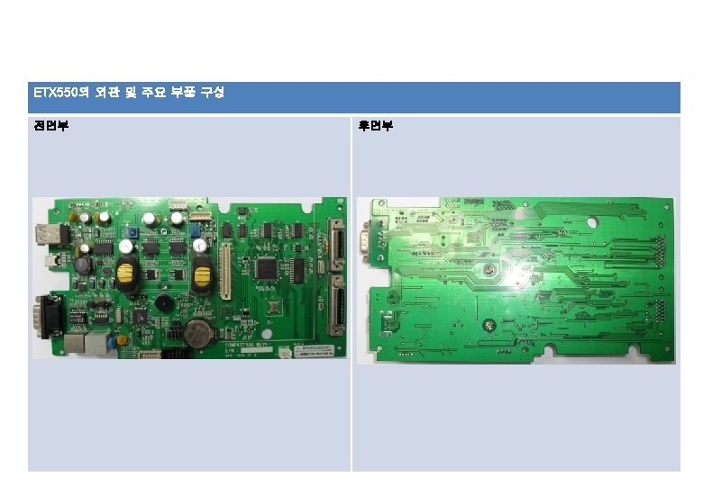
 cpu card의 이해 ETX 550의 외관 및 주요 부품 구성")
 cpu card의 이해 ETX 550의 외관 및 주요 부품 구성")
 cpu card의 이해 적용기종: 소두K 시리즈, 다두 E, SB시리즈, TA,")
 cpu card의 이해 3) ETX 550 CPU BOARD의 주요 부품")
 cpu card의 이해 3) ETX 550 CPU BOARD의 주요 부품")

 LCD PANEL CONNECTOR/DF")
- Slides: 11
SIS(Silicon Integrated Systems ) cpu card의 이해 System Specification CPU Si. S 550 Integrated x 86 / MMX Compatible CPU PC-compatible DMA CONTROLLERS, INTERRUPT CONTROLLERS AND TIMERS MEMORY 32 M SDRAM on Board BIOS KARAM BIOS Display Integrated Ultra-AAGPTM VGA for Hardware 2 D/Video/Graphics Accelerators AGP 4 X Compliant / Fully Direct. X 8 Compliant Built-In DVI / DSTN/VIP interface Support TTL/LVDS panel and CRT Moniter Output RTC Supports ACPI Day-of-Month and Month-of-Year Alarm 256 Bytes Of CMOS SRAM ROM socket One for BIOS and ROM driver BOARD DIMMENSION 100 mm X 70 mm
SIS(Silicon Integrated Systems ) cpu card의 이해 ETX 550의 외관 및 주요 부품 구성 전면부 후면부
SIS(Silicon Integrated Systems ) cpu card의 이해 ETX 550의 외관 및 주요 부품 구성 전면부 후면부 U 16 U 11 U 10 U 8 U 5 U 13 U 7 U 9 U 1 JH 1 Y 2 Y 1
SIS(Silicon Integrated Systems ) cpu card의 이해 적용기종: 소두K 시리즈, 다두 E, SB시리즈, TA, CE시리즈 3) ETX 550 CPU BOARD의 주요 부품 ① SIS 550 (CPU) : U 1 l Integrated x 86 / MMX Compatible CPU l Integrated DRAM Controller l PCI 2. 2 Specification Compliant l Fast PCI 2. 2 Specification Compliant l Integrated Ultra-AGPTM VGA for Hardware 2 D/Video/Graphics Accelerator l Advanced PCI H/W Audio & S/W Modem l Advanced Power Management l Integrated Smart Card Controller l l l ② HY 57 V 283220 T (DRAM) : U 7, U 8 All device pins are Compatible with LVTTL interface 86 TSOP-Ⅱ , 90 Ball FBGA with 0. 8 mm of pin pitch Data mask function by DQM 0, 1, 2, 3 Internal four banks operation Auto refresh and self reflesh 4096 refresh cycle / 64 ms ③ FM 1608 (FRAM) : U 11 l 64 kbit Ferroelectric Nonvolatile RAM l. High Endurance 1 Trillion (1012) Read/Writes l. Year Data Retention l. Advanced High-Reliability Ferroelectric Process l. No Battery concerns l. Low Power Operation l. Industry Standard Configuration 5/20 Page
SIS(Silicon Integrated Systems ) cpu card의 이해 3) ETX 550 CPU BOARD의 주요 부품 ④ ICS 9248 ( Frequency Generator ) : CLK 1 ◇ Output Features : ▷ 3 - CPUs at 2. 5 V ▷ 13 - SDRAM at 3. 3 V ▷ 6 - PCI at 3. 3 V ▷ 2 - AGP at 3. 3 V ▷ 48 MHz at 3. 3 V fixed ▷ 24/48 MHz at 3. 3 V selectable by I 2 C ( Default is 24 MHz ) ▷ REF at 3. 3 V , 14. 318 MHz ◇ Features : ▷ Up to 166 MHz frequincy support ▷ Spread spectrum for EMI control ( 0 to -0. 5% , ± 0. 25% ) ▷ Uses external 14. 318 MHz crystal ⑤ XC 9536 XL (CPLD) : U 61 ▷ 5 ns pin to pin logic delays ▷ Ststem frequincy up to 178 MHz ▷ 36 macrocells with 800 usable gates ▷ Available in small footprint package ▷ 44 -pin VQFP (34 user I/O pin) ▷ Optimized for high-performance 3. 3 V systems (Low power operation) ▷ 5 V tolerant I/O pins accept 5 V , 3. 3 V , 2. 5 V signals
SIS(Silicon Integrated Systems ) cpu card의 이해 3) ETX 550 CPU BOARD의 주요 부품 ⑥ K 9 F 6408 (NAND Flash Memory) : U 60 , U 62 ▷ 3. 3 V device(K 9 F 6408 U 0 C) : 2. 7 V ~ 3. 6 V ▷ Memory Cell Array : (8 M + 256 k)bit x 8 bit ▷ Automatic Program and Erase ▷ Page Program : (512 + 16)Byte ▷ Block Erase : (8 k + 256)Byte ▷ 528 Byte Page Read Operation ▷ Hardware Data Protection ▷ Program/Erase Lockout During Power Transitions ⑦ 24 LC 04 B (Serial EEPROM) : U 9
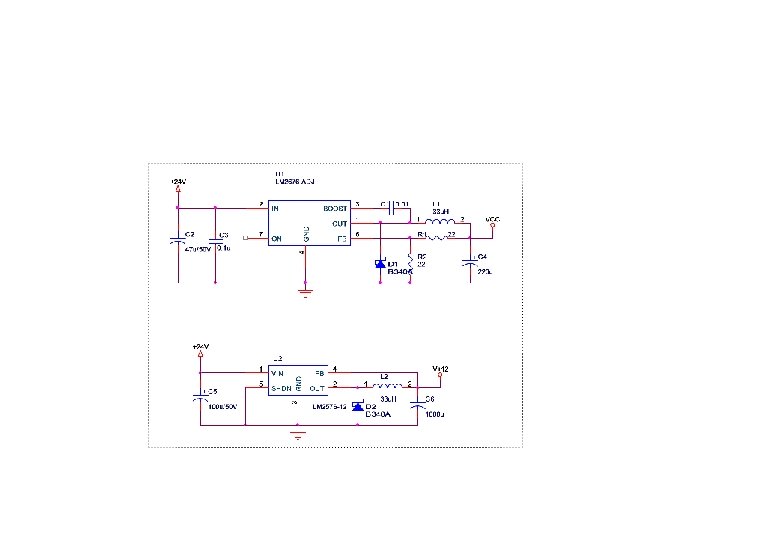
4. Socket & Connector CPU board connector / FX 6 -80 P-0. 8 SV (JH 1) PIN 1 3 5 7 9 11 13 15 17 19 21 23 25 27 29 31 33 35 37 39 41 43 45 47 49 51 53 55 57 59 61 63 65 67 69 71 73 75 77 79 ASSIGNMENT GND SB 3 V PWRTN NC VCC 3 PCIRST LDRQ LFRAME SIRQ INT-A INT-B GND GPIO 4 GPIO 5 GPIO 6 GPIO 7 GND XPMDAT XPMCLK GND LRXP LRXM LLED 0 GND UVN 0 UVP 0 OC#0 UVN 2 UVP 2 OC#2 GND SDAT 10 SDAT 0 BIT CLK GND VCC 1. 8 V PIN 2 4 6 8 10 12 14 16 18 20 22 24 26 28 30 32 34 36 38 40 42 44 46 48 50 52 54 56 58 60 62 64 66 68 70 72 74 76 78 80 ASSIGNMENT GND SB 3 V PSON NC VCC 3 PCICLK 1 LAD 0 LAD 1 LAD 2 LAD 3 RTCVDD GND GPIO 0 GPIO 1 GWR GOOD GND CS 1 KBDAT KBCLK GND LTXP LTXM LLED 1 GND UVN 1 UVP 1 OC#1 VCC VCC GND SPKR AC RETSET SYNC GND VCC 1. 8 V
4. Socket & Connector BIOS / ROM DRIVE SOCKET (J 1) LCD PANEL CONNECTOR/DF 9 -41 P-1 V(J 2) PIN 1 3 5 7 9 11 13 15 17 19 21 23 25 27 29 31 ASSIGNMENT P 01 A 15 A 7 A 5 A 3 A 1 D 0 D 2 D 3 D 5 D 7 A 10 OE A 8 A 14 P 31 PIN 2 4 6 8 10 12 14 16 18 20 22 24 26 28 30 32 ASSIGNMENT A 16 A 12 A 6 A 4 A 2 A 0 D 1 GND D 4 D 6 CE VAD 0 A 9 A 13 A 17 VCC PIN 1 3 5 7 9 11 13 15 17 19 21 23 25 27 29 31 33 35 37 39 41 ASSIGNMENT VAD 8 VAD 4 VAD 9 VAD 5 VAD 10 VAD 6 VAD 11 VAD 7 VCC VAVSYNC DISPOFF VAHSYNC LPCLK 3. 3 V ENABKL LCDVDD ENVEE GND NC PIN 2 4 6 8 10 12 14 16 18 20 22 24 26 28 30 32 34 36 38 40 42 ASSIGNMENT GND VCC VBD 0 VBD 8 VBD 1 VBD 9 VBD 2 VBD 10 VBD 3 VBD 11 VBD 4 VAD 0 VBD 5 VAD 1 VBD 6 VAD 2 VBD 7 VAD 3 12 V