SINGLEBALANCED MIXER PROJECT DESIGN REVIEW RIT Senior Project

SINGLE-BALANCED MIXER PROJECT DESIGN REVIEW RIT Senior Project Jared Burdick Held May 3, 2012 Updated May 5, 2012 with Action Items
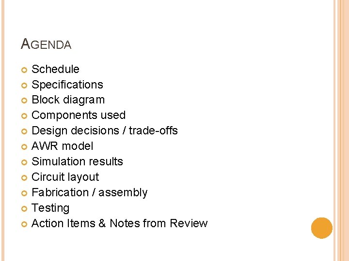
AGENDA Schedule Specifications Block diagram Components used Design decisions / trade-offs AWR model Simulation results Circuit layout Fabrication / assembly Testing Action Items & Notes from Review
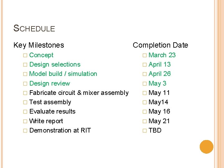
SCHEDULE Key Milestones � Concept � Design selections � Model build / simulation � Design review � Fabricate circuit & mixer assembly � Test assembly � Evaluate results � Write report � Demonstration at RIT Completion Date � March 23 � April 13 � April 26 � May 3 � May 11 � May 14 � May 16 � May 21 � TBD
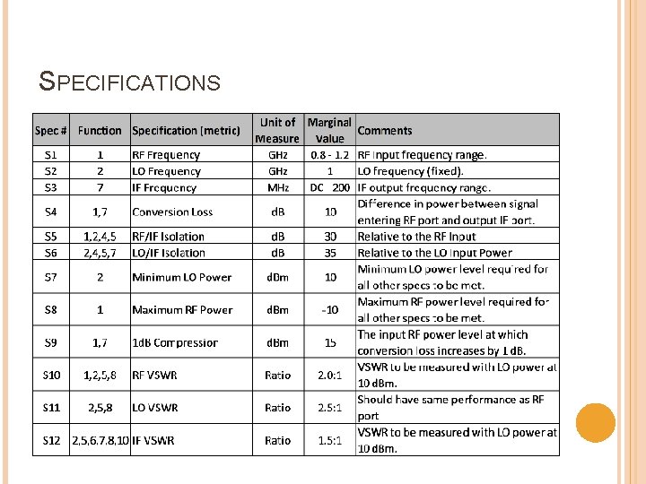
SPECIFICATIONS
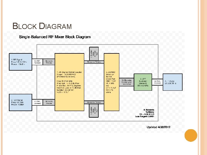
BLOCK DIAGRAM
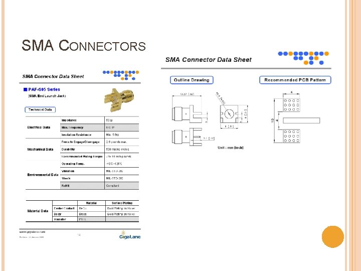
COMPONENT LIST RF splitting (1) � Anaren SMD Hybrid Coupler Diodes (2) � Avago RF Schottky-barrier series pair (1) LPF (1) � Lumped element maximally flat – 5 th order RF connectors (3) � SMA female jack end-launch printed circuit board mount Printed circuit functions (on RO 4003, 32 -mil thick, 1 oz. copper) � RF chokes – shorted λ/4 stub (2) � Impedance transformer - λ/4 (1) � 50Ω lines (5)
SUBSTRATE MATERIAL
HYBRID COUPLER
HYBRID COUPLER
SCHOTTKY DIODES
LOW-PASS FILTER
SMA CONNECTORS
PRINTED LINE CONSIDERATIONS RF chokes Maximized line width vs. performance to gain production margin (narrow linewidths more difficult to produce). � Need to stub is well grounded – brought it close to the edge where a strap can be installed. � Quarter-wave impedance transformer � � � 50Ω interconnects � Meandered to minimize the size of the circuit substrate. Tapered the line where it met component pads. Mitered corners. Grounding Added ground to the top of the circuit board wherever possible to reduce impedance. � Will connect top & and bottom planes with wires and straps. This would normally be accomplished with plated via’s. � Component pads � Used manufacturers’ recommendations.
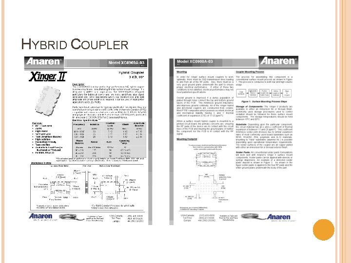
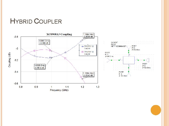
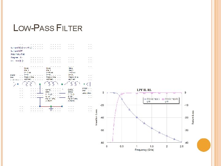
DESIGN DECISIONS MADE / TRADE-OFFS RF Splitting Looked at 90, 180 degree couplers. � 90 -degree easier to implement. � Surface mount standard product readily available from Anaren (distribution) & inexpensive. � Greatly simplifies the circuit board. � Filtering � Removed BPF’s in the RF and LO paths � Not readily available or too expensive. Not enough time to design lumped-element realizations. Not critical to performance or meeting specification. LPF (IF path) Maximally flat – desire good pass-band flatness and suppress the 1. 0 GHz LO leakage. Lumped-element – distributed too large, components are inexpensive. 5 th order (see design and simulation later). Purchase coils, use DLI capacitors.
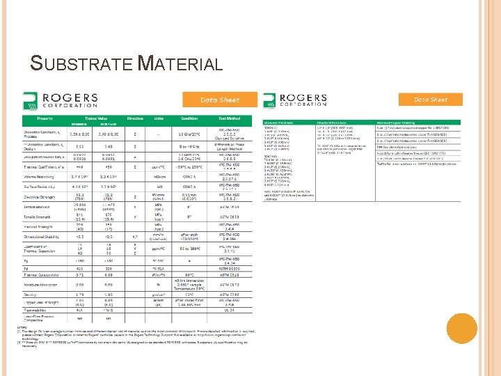
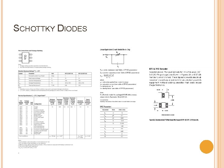
DECISIONS / TRADE-OFFS RF Chokes � Started with radial transformers (λ/2 open stubs). � Moved to λ/4 shorted stubs (high impedance). Diodes � � � Did not simulate very well – higher conversion loss & poor flatness. Avago Schottky series pair diodes selected. Using a pair improve diode match (to each other). Also purchased Infineon pair as a risk reduction (same package so they can be installed on existing circuit). Substrate Material Rogers RO 4003 selected. Low-cost microwave material. FR-4 could potentially be utilized – risk item (higher loss, more εr variation) 32 -mil thickness selected to provide some rigidity for the soldered components and the connectors. � 1 -oz copper used due to soldering, particularly the connectors – fear that 0. 5 oz would tear or lift during hand-solder operations. � �
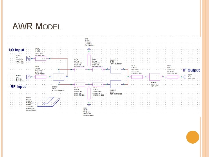
AWR MODEL
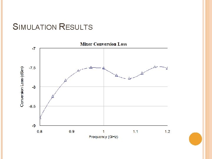
SIMULATION RESULTS
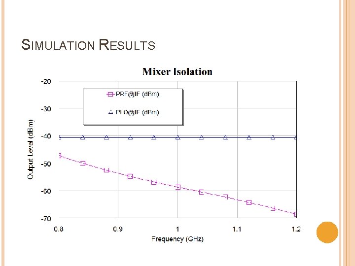
SIMULATION RESULTS
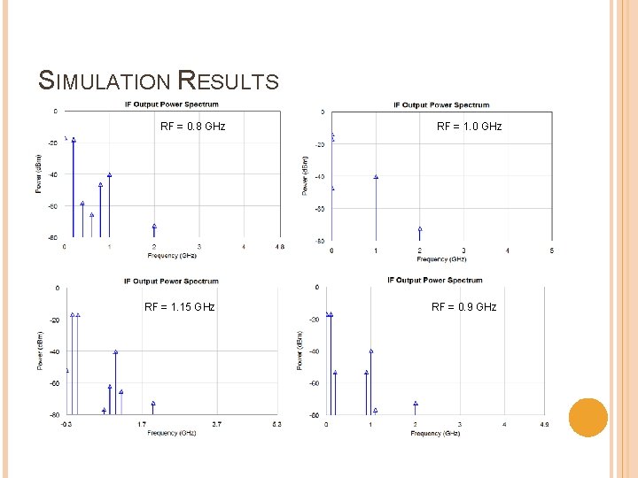
SIMULATION RESULTS RF = 0. 8 GHz RF = 1. 15 GHz RF = 1. 0 GHz RF = 0. 9 GHz
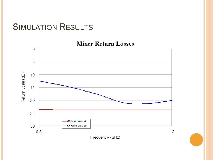
SIMULATION RESULTS
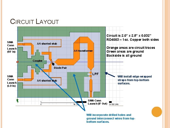
CIRCUIT LAYOUT SMA Conn Launch (RF In) Circuit is 2. 0” x 2. 5” x 0. 032” RO 4003 – 1 oz. Copper both sides λ/4 shorted stub λ/4 transformer Orange areas are circuit traces Green areas are ground Backside is all ground Coupler Diode Pair SMA Conn Launch (LO In) LPF λ/4 shorted stub Will install edge-wrapped straps from top-bottom surfaces. SMA Conn Launch (IF Out) Will incorporate drilled holes and ground interconnect wires from topbottom surfaces.
FABRICATION & ASSEMBLY Circuit to be fabricated at Anaren using LPKF prototype circuit router. Approximately 4 circuits will be produced initially – more if needed. � Will require some hand de-burring of copper. � Inside corners will not be 90 -degrees, there will be a small radius base on the diameter of the end-mill used. � The small gap for the LPF shunt capacitors may have to be hand cut with a scalpel. � Circuit assembly will be performed by Anaren Assembly Technician Basic soldering of components using manufacturer’s recommendations where possible (recommended footprints were incorporated in the design/layout). � Manual soldering of ground connections from top to bottom copper layers using: � Edge-wraps Wires through drilled holes.
TESTING Testing to be performed at Anaren � � � Test Equipment Required � � � Conversion Loss Isolations (RF-IF, LO-IF) VSWR’s (RF, LO, IF ports) 1 -d. B Compression Spurious Response Spectrum Analyzer RF Signal Generators (2) Power Meter SMA Male 50Ω Terminations (2) Test Cables (3) Adapters (as required) Sample Size One piece initially � Additional (1 -3) after �
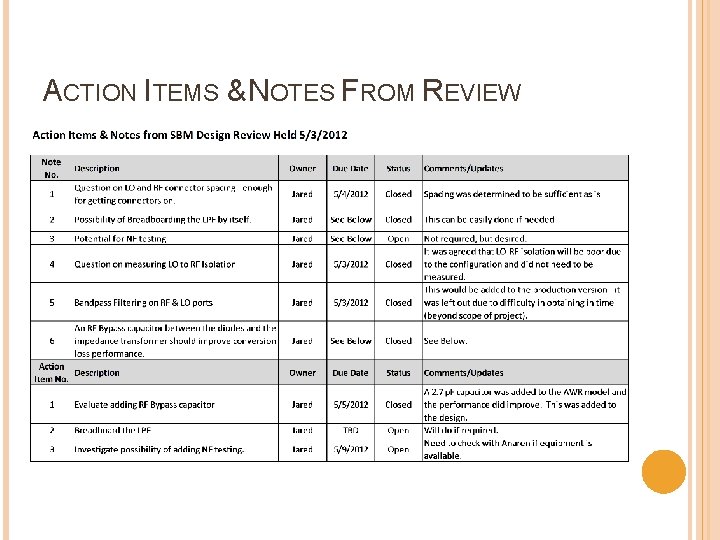
ACTION ITEMS & NOTES FROM REVIEW
- Slides: 24