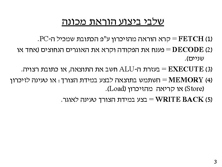
Single cycle data paths Processor uses synchronous logic

. f T 1")


 Built out of an array of 32 flip-flops Din")
 32 A+B + 32 B op 32")


 5 Why is R 0 special? R 0 - The")
? If we had")

![Animating the Datapath Instruction <- MEM[PC] PC <- PC + 4](https://slidetodoc.com/presentation_image/3faf279251f66c2f99161633f855599b/image-19.jpg "Animating the Datapath Instruction <- MEM[PC] PC <- PC + 4")

![Animating the Datapath add rd, rs, rt R[rd] <- R[rs] + R[rt](https://slidetodoc.com/presentation_image/3faf279251f66c2f99161633f855599b/image-21.jpg "Animating the Datapath add rd, rs, rt R[rd] <- R[rs] + R[rt")

![Animating the Datapath lw rt, offset(rs) R[rt] <- MEM[R[rs] + s_extend(o](https://slidetodoc.com/presentation_image/3faf279251f66c2f99161633f855599b/image-23.jpg "Animating the Datapath lw rt, offset(rs) R[rt] <- MEM[R[rs] + s_extend(o")
![Animating the Datapath sw rt, offset(rs) MEM[R[rs] + sign_extend(offset)]](https://slidetodoc.com/presentation_image/3faf279251f66c2f99161633f855599b/image-24.jpg "Animating the Datapath sw rt, offset(rs) MEM[R[rs] + sign_extend(offset)]")

![Animating the Datapath beq rs, rt, offset if (R[rs] == R[rt]) then PC <-](https://slidetodoc.com/presentation_image/3faf279251f66c2f99161633f855599b/image-26.jpg "Animating the Datapath beq rs, rt, offset if (R[rs] == R[rt]) then PC <-")
 or sign-extended lower half of")

")
")


")
")


![? איך זה נראה בספר 4 Adde r [31: 26] 6 PC Instruction Memory](https://slidetodoc.com/presentation_image/3faf279251f66c2f99161633f855599b/image-42.jpg "? איך זה נראה בספר 4 Adde r [31: 26] 6 PC Instruction Memory")
![? איך זה נראה בספר 4 Adde r [31: 26] 6 PC Instruction Memory](https://slidetodoc.com/presentation_image/3faf279251f66c2f99161633f855599b/image-43.jpg "? איך זה נראה בספר 4 Adde r [31: 26] 6 PC Instruction Memory")
![? איך זה נראה בספר 4 Adde r [31: 26] 6 PC Instruction Memory](https://slidetodoc.com/presentation_image/3faf279251f66c2f99161633f855599b/image-44.jpg "? איך זה נראה בספר 4 Adde r [31: 26] 6 PC Instruction Memory")


 Syntax: SW $3,")

![A CPU capable of lw instructions only 4 Adde r [31: 26] 6 add](https://slidetodoc.com/presentation_image/3faf279251f66c2f99161633f855599b/image-51.jpg "A CPU capable of lw instructions only 4 Adde r [31: 26] 6 add")
![A CPU capable of lw instructions only 4 Adde r [31: 26] 6 add](https://slidetodoc.com/presentation_image/3faf279251f66c2f99161633f855599b/image-52.jpg "A CPU capable of lw instructions only 4 Adde r [31: 26] 6 add")

![A CPU capable of R-type & lw instructions (principle) 4 Adde r [31: 26]](https://slidetodoc.com/presentation_image/3faf279251f66c2f99161633f855599b/image-54.jpg "A CPU capable of R-type & lw instructions (principle) 4 Adde r [31: 26]")
![A CPU capable of R-type & lw instructions 4 Adde r [31: 26] 6](https://slidetodoc.com/presentation_image/3faf279251f66c2f99161633f855599b/image-55.jpg "A CPU capable of R-type & lw instructions 4 Adde r [31: 26] 6")


")

![Control 0 M u x Add 4 Instruction [31– 26] PC Instruction memory Instruction](https://slidetodoc.com/presentation_image/3faf279251f66c2f99161633f855599b/image-63.jpg "Control 0 M u x Add 4 Instruction [31– 26] PC Instruction memory Instruction")


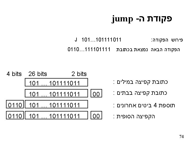
![Jump Instruction [25– 0] 26 Shift left 2 Jump address [31– 0] 28 0](https://slidetodoc.com/presentation_image/3faf279251f66c2f99161633f855599b/image-67.jpg "Jump Instruction [25– 0] 26 Shift left 2 Jump address [31– 0] 28 0")
- Slides: 67
Single cycle data paths Processor uses synchronous logic design (a “clock”). f T 1 MHz 1 μs 10 MHz 100 ns 100 MHz 10 ns 1 GHz 1 ns D All state elements act like positive edgetriggered flip flops. clk Q 5
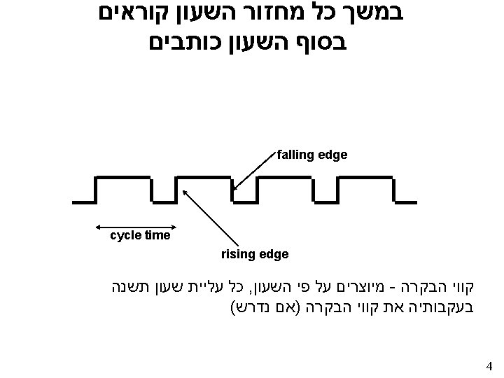
Edge-Triggered D Flip Flops D Q Value of D is sampled on positive clock edge. Q outputs sampled value for rest of cycle. CLK D Q 6
Single cycle data paths: Definition All instructions execute in a single cycle of the clock (positive edge to positive edge) Advantage: a great way to learn CPUs. Drawbacks: unrealistic hardware assumptions, slow clock period 7
Recall: MIPS R-format instructions Syntax: ADD $8 $9 $10 Instruction Fetch Instruction Decode Operand Fetch Execute Result Store Next Instruction Semantics: $8 = $9 + $10 Fetch next inst from memory: 012 A 4020 opcode rs rt rd shamt funct Decode fields to get : ADD $8 $9 $10 “Retrieve” register values: $9 $10 Add $9 to $10 Place this sum in $8 Prepare to fetch instruction that follows the ADD in the program. 8
Separate Read-Only Instruction Memory זכרון פקודות 32 Data Reads are combinational: Put a stable address on input, a short time later data appears on output. Addr 32 טעינת התוכנית לזכרון לא מעניננו כרגע זכרון )מטמון( נפרד לפקודות ולנתונים Instruction Memory ) ( Data Memory & 9
1 שלב : Straight-line Instruction Fetch Instr Mem 32 Data Addr 32 Fetching straight-line MIPS instructions requires a machine that generates this timing diagram: Why do we increment every clock cycle? Why +4 and not +1? CLK Addr Data PC PC + 4 IMem[PC] IMem[PC + 4] PC + 8 IMem[PC + 8] PC == Program Counter, points to next instruction. 10
Single-cycle Implementation of MIPS • Our first implementation of MIPS will use a single long clock cycle for every instruction • Every instruction begins on one up (or, down) clock edge and ends on the next up (or, down) clock edge • This approach is not practical as it is much slower than a multicycle implementation where different instruction classes can take different numbers of cycles – in a single-cycle implementation every instruction must take the same amount of time as the slowest instruction – in a multicycle implementation this problem is avoided by allowing quicker instructions to use fewer cycles • Even though the single-cycle approach is not practical it is simple and useful to understand first • Note : we shall implement jump at the very end
New Component: Register (for PC) Built out of an array of 32 flip-flops Din 0 D Q Dout 0 Din 1 D Q Dout 1 Din 2 D Q Dout 2 PC 32 32 Din Dout Clk In later examples, we will add an “enable” input: clock edge updates state only if enable is high clk 12
New Component: A 32 -bit adder (ALU) 32 A+B + 32 B op 32 ln(#ops) 32 A L U ALU: כנ"ל רק למס פונקציות רבות . op לפי הבורר A B Combinational: היציאה שווה לסכום ערכי B- ו A כניסה . ( מלפני זמן קצר )~ ננו שניה 32 A op B Zero? Sometimes, extra outputs for use by control logic 13
Design: Straight-line Instruction Fetch State machine design in the service of an ISA 32 PC 32 + Instr Mem 32 32 D Q 32 Addr Data 32 0 x 4 +4 in hexadecimal Clk CLK Addr Data PC PC + 4 IMem[PC] IMem[PC + 4] PC + 8 IMem[PC + 8] 14
Goal #1: An R-format single-cycle CPU Syntax: ADD $8 $9 $10 Instruction Fetch Instruction Decode Operand Fetch Execute Result Store Next Instruction Semantics: $8 = $9 + $10 Done! To continue, we need registers. . . Fetch next inst from memory: 012 A 4020 opcode rs rt rd shamt funct Decode fields to get : ADD $8 $9 $10 “Retrieve” register values: $9 $10 Add $9 to $10 Place this sum in $8 Prepare to fetch instruction that follows the ADD in the program. 15
Register files: clk sel(ws) 5 Why is R 0 special? R 0 - The constant 0 D D E WE M U. . . X D En En R 1 R 2 “two read ports” sel(rs 1) Q 32. . . Q Q . . . sel(rs 2) 32 D R 31 Q . . . 32 wd M 32 rd 1 U X 32 . . . En 5 5 M 32 rd 2 U X 32 16
Register File Schematic Symbol Why do we need WE (Write Enable)? If we had a register file w/o WE, how could we work around it? 5 5 Reg. File rs 1 rs 2 5 ws wd 32 32 rd 1 rd 2 32 WE 17
Datapath: Instruction Store/Fetch & PC Increment Three elements used to store and fetch instructions and increment the PC Datapath
Animating the Datapath Instruction <- MEM[PC] PC <- PC + 4
Datapath: R-Type Instruction Two elements used to implement R-type instructions Datapath
Animating the Datapath add rd, rs, rt R[rd] <- R[rs] + R[rt
Datapath: Load/Store Instruction Two additional elements used To implement load/stores Datapath
Animating the Datapath lw rt, offset(rs) R[rt] <- MEM[R[rs] + s_extend(o
Animating the Datapath sw rt, offset(rs) MEM[R[rs] + sign_extend(offset)]
Datapath: Branch Instruction No shift hardware required: simply connect wires from input to output, each shifted left 2 bits Datapath
Animating the Datapath beq rs, rt, offset if (R[rs] == R[rt]) then PC <- PC+4 + s_exten
MIPS Datapath I: Single-Cycle Input is either register (R-type) or sign-extended lower half of instruction (load/store) Data is either from ALU (R-type) or memory (load) Combining the datapaths for R-type instructions and load/stores using two multiplexors
Animating the Datapath: R-type Instruction add rd, rs, rt
Animating the Datapath: Load Instruction lw rt, offset(rs)
Animating the Datapath: Store Instruction sw rt, offset(rs)
MIPS Datapath II: Single-Cycle Separate adder as ALU operations and PC increment occur in the same clock cycle Separate instruction memory as instruction and data read occur in the same clock cycle Adding instruction fetch
MIPS Datapath III: Single-Cycle New multiplexor Extra adder needed as both adders operate in each cycle Instruction address is either PC+4 or branch target address Adding branch capability and another multiplexor Important note: in a single-cycle implementation data cannot be stored during an instruction – it only moves through combinational logic Question: is the Mem. Read signal really needed? ! Think of Reg. Write…!
Datapath Executing add rd, rs, rt
Datapath Executing lw lw rt, offset(rs)
Datapath Executing sw sw rt, offset(rs)
Datapath Executing beq r 1, r 2, offset
Goal #1: An R-format single-cycle CPU Syntax: ADD $8 $9 $10 Instruction Fetch Instruction Decode Operand Fetch Execute Result Store Next Instruction Semantics: $8 = $9 + $10 What do we do with these? Fetch next inst from memory: 012 A 4020 opcode rs rt rd shamt funct Decode fields to get : ADD $8 $9 $10 “Retrieve” register values: $9 $10 Add $9 to $10 Place this sum in $8 Prepare to fetch instruction that follows the ADD in the program. 37
Computing engine of the R-format CPU Decode fields to get : ADD $8 $9 $10 opcode rs rt rd shamt funct Logic op 5 5 rs 1 rs 2 5 ws wd 32 32 Reg. File 32 rd 1 rd 2 32 32 A L U 32 WE What do we do with WE? 38
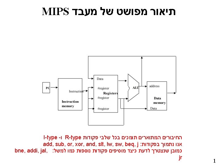
Putting it all together. . . 32 PC Instr Mem 32 32 32 D + Q 32 Addr Data 32 To rs 1, rs 2, ws, op decode logic. . . 0 x 4 Is it safe to use same clock for PC and Reg. File? 5 5 rs 2 5 ws wd 32 op 32 Reg. File rs 1 Logic 32 rd 1 rd 2 32 32 A L U 32 WE 39
Reminder: How data flows after posedge Instr Mem PC D + Q Addr Data 0 x 4 Logic op 5 5 rs 1 rs 2 5 ws wd 32 32 Reg. File 32 rd 1 rd 2 32 32 A L U 32 WE 40
Next posedge: Update state and repeat PC D 5 5 Reg. File rs 1 rs 2 5 ws wd 32 Q 32 rd 1 rd 2 32 WE 41
? איך זה נראה בספר 4 Adde r [31: 26] 6 PC Instruction Memory [25: 21]=Rs 5 [20: 16]=Rt 5 [15: 11]=Rd 5 ck [5: 0]=funct 6 A CPU capable of R-type instructions only 42
? איך זה נראה בספר 4 Adde r [31: 26] 6 PC Instruction Memory Reg File [25: 21]=Rs 5 ALU [20: 16]=Rt 5 [15: 11]=Rd 5 ck [5: 0]=funct 6 ck A CPU capable of R-type instructions only 45
? איך זה נראה בספר 4 Adde r [31: 26] 6 PC Instruction Memory Reg File [25: 21]=Rs 5 ALU [20: 16]=Rt 5 [15: 11]=Rd 5 ck [5: 0]=funct 6 ck A CPU capable of R-type instructions only 46
I-format ALU instructions : 2 יעד מס Syntax: ORI $8 $9 64 Semantics: $8 = $9 | 64 In this example, $8 (the result register) is rt !!! (was rd previously). 16 -bit immediate extended to 32 bits. Zero-extend: 0 x 8000 ⇨ 0 x 00008000 Sign-extend: 0 x 8000 ⇨ 0 x. FFFF 8000 Some MIPS instructions zero-extend immediate field, other instructions sign- 52
Computing engine of the I-format CPU Decode fields to get : ORI $8 $9 64 Logic op 32 5 5 Reg. File rs 1 rs 2 5 ws wd 32 32 rd 1 rd 2 32 Ext 32 A L U 32 WE In a Verilog implementation, what should we do with 53 rs 2?
Merging data paths. . . Add muxes How many ? R-format I-format Where ? 54
The merged data path. . . opcode rs rt rd shamt funct ALUctr op 5 5 rs 1 rs 2 5 ws wd Reg. Dest 32 32 Reg. File 32 rd 1 rd 2 32 32 A L U 32 WE Ext. Op ALUsrc 55
Loads, Stores, and Data Memory. . . Syntax: LW $1, 32($2) Syntax: SW $3, 12($4) Action: $1 = M[$2 + 32] Action: M[$4 + 12] = $3 32 Zero-extend or sign-extend immediate field? Data Memory Reads are combinational: Addr 32 Put a stable address on Addr, Dout a short time later Dout is ready Din 32 WE Writes are clocked: If WE is high, memory Addr captures Din on positive edge of clock. Note: Not a realistic main memory (DRAM) model. . . 57
? CPU - איפה ה Instruction Memory CPU PC Data Memory 58
A CPU capable of lw instructions only 4 Adde r [31: 26] 6 add Reg. Write=1 Reg File PC Instruction Memory [25: 21]=Rs 5 Data Memory ALU [20: 16]=Rt 5 Address D. Out 5 ck ck [15: 0] 16 Sext 16 ->32 59
A CPU capable of lw instructions only 4 Adde r [31: 26] 6 add Reg. Write=1 Reg File PC Instruction Memory [25: 21]=Rs 5 Data Memory ALU [20: 16]=Rt 5 Address D. Out 5 ck ck [15: 0] 16 Sext 16 ->32 60
A CPU capable of lw & sw instructions only 4 Me. Write=1 Adde r [31: 26] 6 add Reg. Write=0 Reg File PC Instruction Memory [25: 21]=Rs 5 Data Memory ALU [20: 16]=Rt 5 Address 5 D. In ck ck [15: 0] 16 Sext 16 ->32 61
A CPU capable of R-type & lw instructions (principle) 4 Adde r [31: 26] 6 add Reg. Write [5: 0]=funct 6 ALU control Reg File PC Instruction Memory [25: 21]=Rs 5 Data Memory ALU [20: 16]=Rt 5 Address [15: 11]=Rd 5 ck ck [15: 0] 16 Sext 16 ->32 62
A CPU capable of R-type & lw instructions 4 Adde r [31: 26] 6 add Reg. Write [5: 0]=funct 6 ALU control Reg File PC Instruction Memory [25: 21]=Rs 5 Data Memory ALU [20: 16]=Rt 5 Address D. Out 5 Rd ck [15: 0] 16 ck Sext 16 ->32 63
A CPU capable of R-type & lw/sw instructions 4 Mem. Write Adde r [31: 26] 6 add Reg. Write [5: 0]=funct 6 ALU control Reg File PC Instruction Memory [25: 21]=Rs 5 Data Memory ALU [20: 16]=Rt 5 Address D. Out 5 D. In Rd ck [15: 0] 16 ck Sext 16 ->32 64
Conditional Branches in MIPS. . . Syntax: BEQ $1, $2, 12 Action: If ($1 != $2), PC = PC + 4 Action: If ($1 == $2), PC = PC + 48 Immediate field codes # words, not # bytes. Why is this encoding a good idea? Zero-extend or sign-extend immediate field? 65
אלמנטים דרושים להוספת : Branch Fetch - משלב ה PC+4 Adder In addresses, we always shift left by two bits Read register 1 Read register 2 Instruction Write register Write Data 16 Sum Shift left 2 Branch Target Read data 1 Registers Read data 2 Sigh Extend 32 Zero ALU מועבר ליחידת הבקרה כתוצאה הלוגית של ההשוואה 66
Design: Instruction Fetch with Branch Syntax: BEQ $1, $2, 12 Action: If ($1 != $2), PC = PC + 4 Action: If ($1 == $2), PC = PC + 48 32 PC Instr Mem 32 32 32 D + Q 32 0 x 4 Addr Data 32 32 PCSrc Ex te nd Clk + 32 67
שילוב כל הפקודות M u x ALU Add result 4 PC Read address Instruction memory Shift left 2 Read register 1 Read register 2 Write Read data 1 Zero ALU Registers Write register Write Data ADD M u x Read data 2 result ALU Read address Write address Read data M u x Data memory Write data Read 16 Sign extend 32 68
What is single cycle control? Instr Mem Combinational Logic (Only Gates, No Flip Flops) Equal 32 Addr Just specify logic functions! Data Reg. Dest PCSrc Reg. Wr Ext. Op Mem. To. Reg Mem. Wr ALUsrc 5 5 Reg. File rs 1 rs 2 5 ws wd Reg. Dest 32 ALUctr 32 rd 1 rd 2 32 Equal WE Ext Reg. Wr Ext. Op Mem. To. Reg ALUsrc Mem. Wr 69
קווי בקרה PCSrc 4 Shift left 2 PC Read address Instruction memory M u x Add Registers Read register 1 Read data 1 register 2 Write register Write data Reg. Write 16 ALUSrc Read data 2 Sign extend M u x 32 ALU result 3 ALU operation Zero ALU result Mem Write Memto. Reg Address Write data Read data Data memory M u x Mem. Read 70
Control 0 M u x Add 4 Instruction [31– 26] PC Instruction memory Instruction [15– 11] Zero ALU result Address Read register 1 Instruction [20– 16] Instruction [31– 0] 1 Shift left 2 Reg. Dst Branch Mem. Read Memto. Reg Control ALUOp Mem. Write ALUSrc Reg. Write Instruction [25– 21] Read address ALU Add result 0 M u x 1 Read data 1 Read register 2 Registers Read Write data 2 register 0 M u x 1 Write data Instruction [15– 0] 16 Sign extend d Rea a dat Data memory 1 M u x 0 32 ALU control Instruction [5– 0] 71
Control 72
ALU control output 000 AND 001 OR 010 add 110 subtract 111 set-on-less-than (sign of rs-rt -> rd) 00 = lw, sw 01 = beq, 10 = arithmetic ALUop 73
Jump Instruction [25– 0] 26 Shift left 2 Jump address [31– 0] 28 0 1 M u x ALU Add result 1 0 Zero ALU result Address PC+4 [31– 28] Add 4 Instruction [31– 26] PC Instruction [25– 21] Read address Read register 1 Instruction [20– 16] Instruction [31– 0] Instruction memory Control Instruction [15– 11] Shift left 2 Reg. Dst Jump Branch Mem. Read Memto. Reg ALUOp Mem. Write ALUSrc Reg Write 0 M u x 1 Read data 1 Read register 2 Registers Read Write data 2 register 0 M u x 1 Write data Instruction [15– 0] 16 Sign extend Read data Data memory 1 M u x 0 32 ALU control Instruction [5– 0] 75