Simulation Of The Electrostatic Field Distribution In A
Simulation Of The Electrostatic Field Distribution In A Pixel Device (update) Marina, Artuso Chaouki, Boulahouache Phys. Dept. Syracuse University January 22, 2001 Chaouki, Boulahouache
Goals Of The Simulation Ø Ø Determination of the electrostatic field properties of a pixel device in both p-stop and p-spray configuration. Assess radiation damage before and after irradiation such that we, Optimize the pixel structure so that the lateral field is minimized(to avoid impact ionization and avalanche break down). v Get a feeling how the surface charge density does affect both isolations. v Determine the efficiency of charge collection and dynamical properties influencing charge sharing. v January 22, 2001 Chaouki, Boulahouache 2
Outline… Things to be discussed in this presentation, ü The field distribution for p-stop and p-spray pixels before & after irradiation. ü The comparison between lateral field distributions in both cases. ü The surface charge density dependence of the electric field of p-spray isolation technique, and a qualitative comparison with results obtained from an article titled, “HERA-B Detectors With P-spray Isolation On The N-side” done by Kari S. H. , Trond W. and Berit S. A. n January 22, 2001 Chaouki, Boulahouache 3
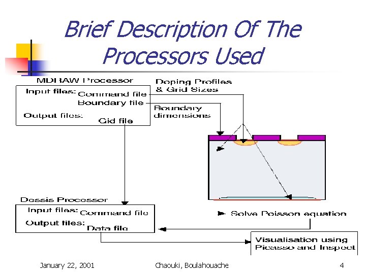
Brief Description Of The Processors Used January 22, 2001 Chaouki, Boulahouache 4
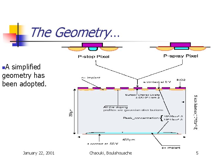
The Geometry… A simplified geometry has been adopted. n January 22, 2001 Chaouki, Boulahouache 5
Grid size… n A finite element analysis requires a grid size input, we have adopted the following: For the height, Ø Maximum height = 0. 24 mm Ø Minimum height = 0. 12 mm For the width, Ø Maximum width = 0. 24 mm Ø Minimum width = 0. 12 mm and this is over a region of 100 mm of width and 9 mm of depth. January 22, 2001 Chaouki, Boulahouache 6
P-stop And P-spray Pixels n n We will study the P-stop and P-spray pixels where the basic structure is the same except that the doping distribution differs. We used a depth of 1. 75 mm for Pstop pixels(as obtained from SINTEF measurement. ), and 1 mm for P-spray pixels. An approximate structure to the graded p-spray will be investigated. January 22, 2001 Chaouki, Boulahouache 7
Surface charge density and Substrate… n Ø Ø Before irradiation, The substrate is of an n-type with a 2 e+12/cm-3 concentration. The surface charge density is about 3 e+11 /cm-2. To model the irradiation effect we have to change the following parameters, The substrate changes to a p-type with a 9 e+12/cm-3 concentration. The surface charge density increases to 5 e+14 /cm-2. January 22, 2001 Chaouki, Boulahouache 8
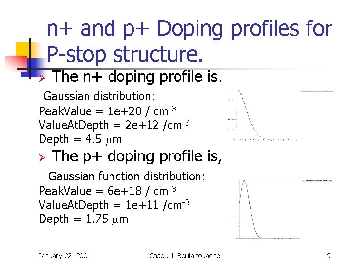
n+ and p+ Doping profiles for P-stop structure. Ø The n+ doping profile is, Gaussian distribution: Peak. Value = 1 e+20 / cm-3 Value. At. Depth = 2 e+12 /cm-3 Depth = 4. 5 mm Ø The p+ doping profile is, Gaussian function distribution: Peak. Value = 6 e+18 / cm-3 Value. At. Depth = 1 e+11 /cm-3 Depth = 1. 75 mm January 22, 2001 Chaouki, Boulahouache 9
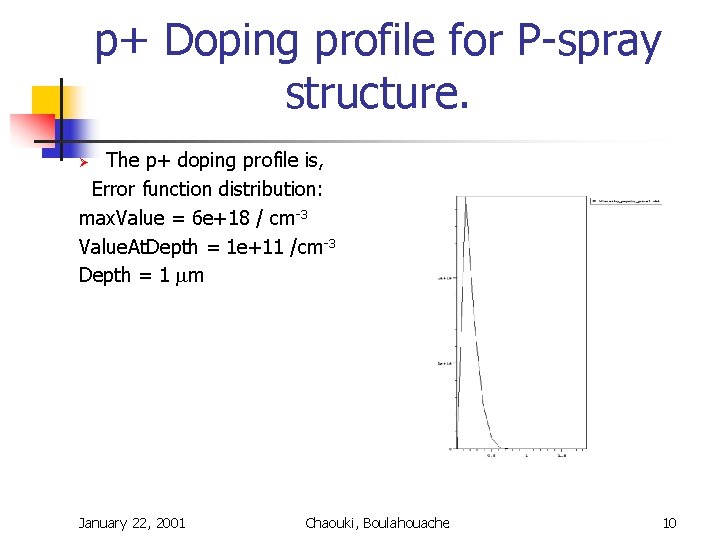
p+ Doping profile for P-spray structure. The p+ doping profile is, Error function distribution: max. Value = 6 e+18 / cm-3 Value. At. Depth = 1 e+11 /cm-3 Depth = 1 mm Ø January 22, 2001 Chaouki, Boulahouache 10
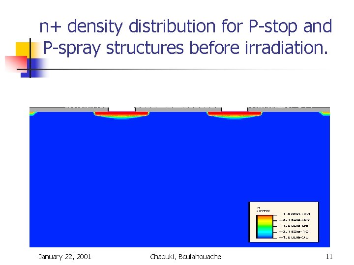
n+ density distribution for P-stop and P-spray structures before irradiation. January 22, 2001 Chaouki, Boulahouache 11
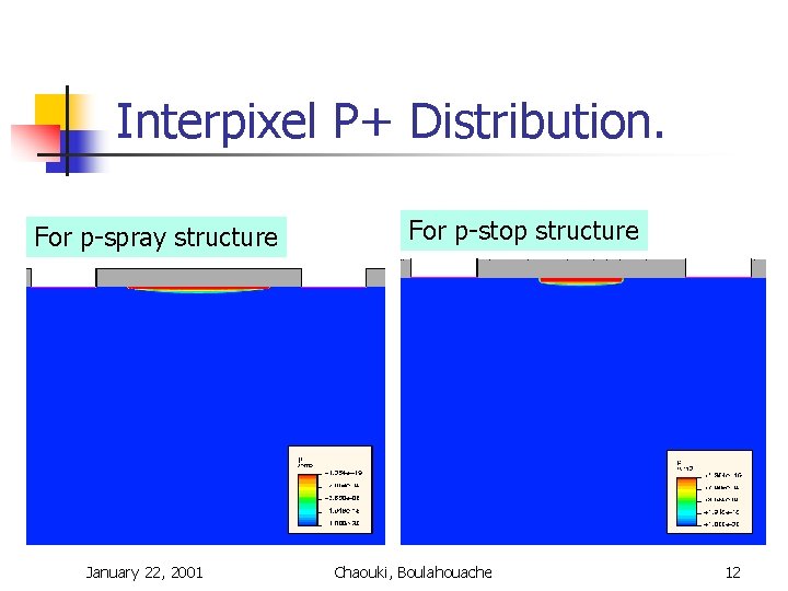
Interpixel P+ Distribution. For p-spray structure January 22, 2001 For p-stop structure Chaouki, Boulahouache 12
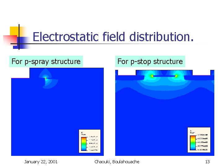
Electrostatic field distribution. For p-spray structure January 22, 2001 For p-stop structure Chaouki, Boulahouache 13
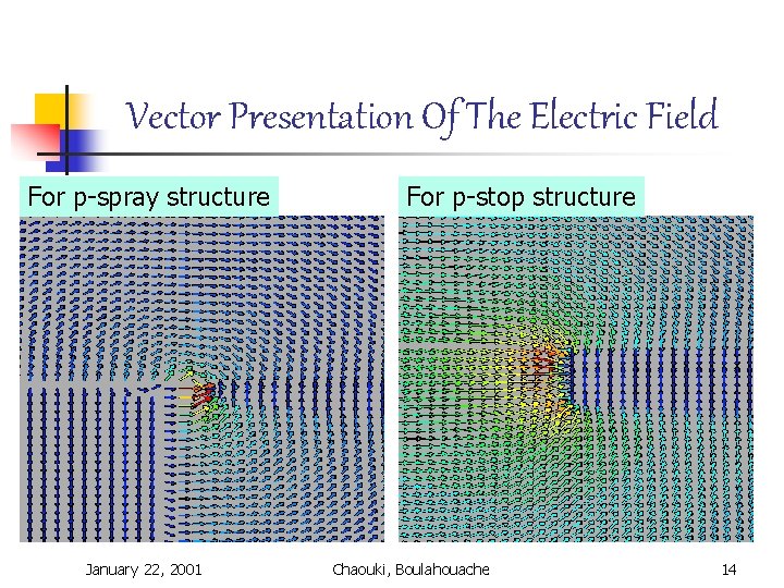
Vector Presentation Of The Electric Field For p-spray structure January 22, 2001 For p-stop structure Chaouki, Boulahouache 14
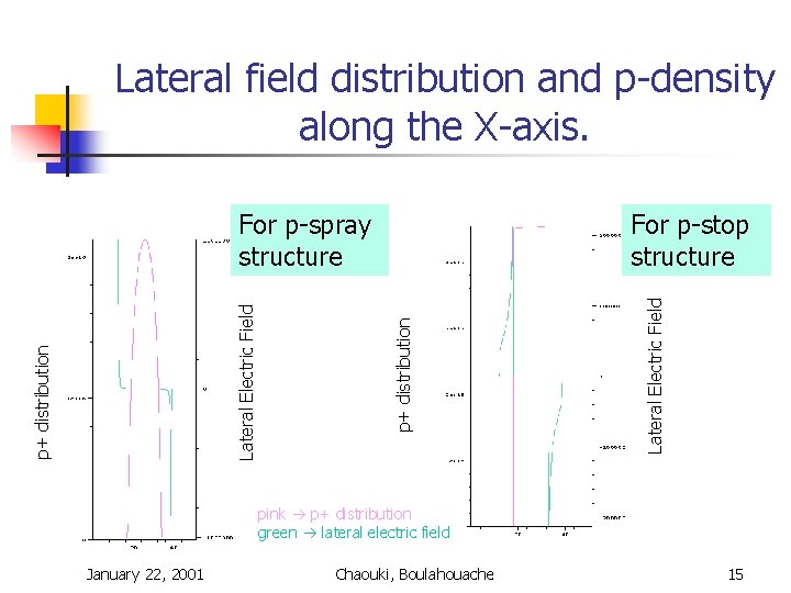
Lateral field distribution and p-density along the X-axis. Lateral Electric Field For p-stop structure p+ distribution Lateral Electric Field For p-spray structure pink p+ distribution green lateral electric field January 22, 2001 Chaouki, Boulahouache 15
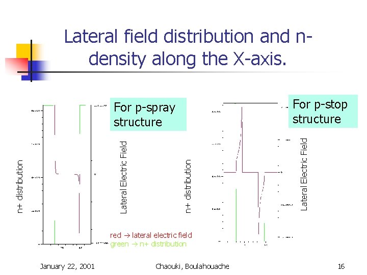
Lateral field distribution and ndensity along the X-axis. n+ distribution Lateral Electric Field For p-stop structure For p-spray structure red lateral electric field green n+ distribution January 22, 2001 Chaouki, Boulahouache 16
Characteristics of the lateral field (Before irradiation) n Ø Ø Before irradiation the maximum lateral field, For p-stop structure is 2. 277 e+05 V/cm which is a factor of 1. 9 higher than the number given in a paper done by Rohe et al. paper*. For p-spray structure is 1. 719 e+06 V/cm which is a factor of 4. 5 higher than the number given in the same paper. *Rohe et al. / Nucl. Instr. And Meth. In January 22, 2001 Phys. Res. A 409 (1998) 224 -228. Chaouki, Boulahouache 17
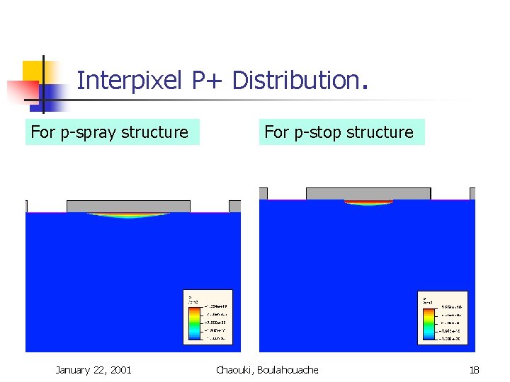
Interpixel P+ Distribution. For p-spray structure January 22, 2001 For p-stop structure Chaouki, Boulahouache 18
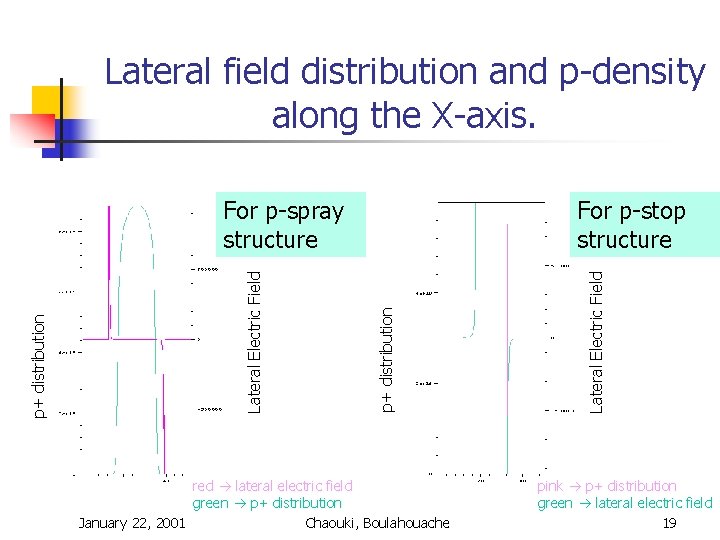
Lateral field distribution and p-density along the X-axis. red lateral electric field green p+ distribution January 22, 2001 Chaouki, Boulahouache Lateral Electric Field For p-stop structure p+ distribution Lateral Electric Field p+ distribution For p-spray structure pink p+ distribution green lateral electric field 19
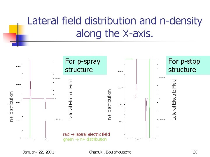
Lateral field distribution and n-density along the X-axis. Lateral Electric Field For p-stop structure n+ distribution Lateral Electric Field For p-spray structure red lateral electric field green n+ distribution January 22, 2001 Chaouki, Boulahouache 20
Characteristics of the lateral field (after irradiation) n Ø Ø After irradiation the maximum lateral field, For p-stop structure is 1. 263 e+06 V/cm which is a factor of 2. 6 higher than the number given in Rohe paper. For p-spray structure is 1. 200 e+06 V/cm which is a factor of 6 higher. January 22, 2001 Chaouki, Boulahouache 21
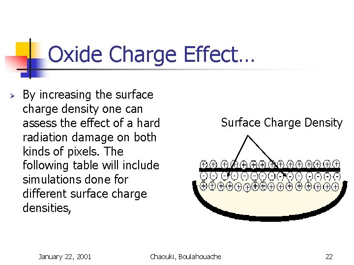
Oxide Charge Effect… Ø By increasing the surface charge density one can assess the effect of a hard radiation damage on both kinds of pixels. The following table will include simulations done for different surface charge densities, January 22, 2001 Chaouki, Boulahouache Surface Charge Density 22
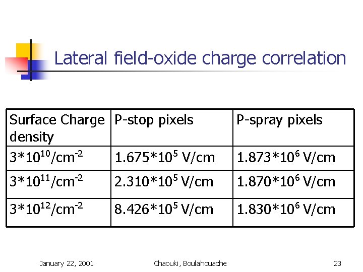
Lateral field-oxide charge correlation Surface Charge P-stop pixels density 3*1010/cm-2 1. 675*105 V/cm P-spray pixels 3*1011/cm-2 2. 310*105 V/cm 1. 870*106 V/cm 3*1012/cm-2 8. 426*105 V/cm 1. 830*106 V/cm January 22, 2001 Chaouki, Boulahouache 1. 873*106 V/cm 23
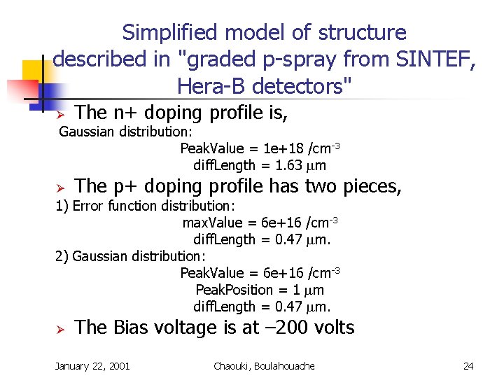
Simplified model of structure described in "graded p-spray from SINTEF, Hera-B detectors" Ø The n+ doping profile is, Gaussian distribution: Peak. Value = 1 e+18 /cm-3 diff. Length = 1. 63 mm Ø The p+ doping profile has two pieces, 1) Error function distribution: max. Value = 6 e+16 /cm-3 diff. Length = 0. 47 mm. 2) Gaussian distribution: Peak. Value = 6 e+16 /cm-3 Peak. Position = 1 mm diff. Length = 0. 47 mm. Ø The Bias voltage is at – 200 volts January 22, 2001 Chaouki, Boulahouache 24
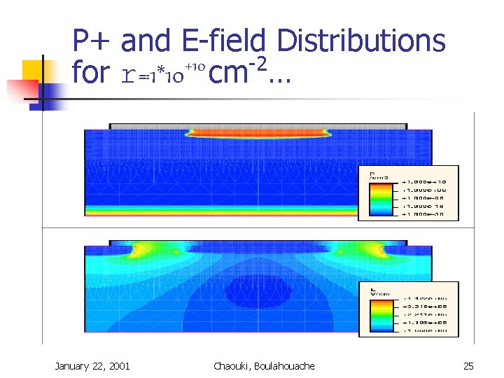
P+ and E-field Distributions +10 -2 for r=1*10 cm … January 22, 2001 Chaouki, Boulahouache 25
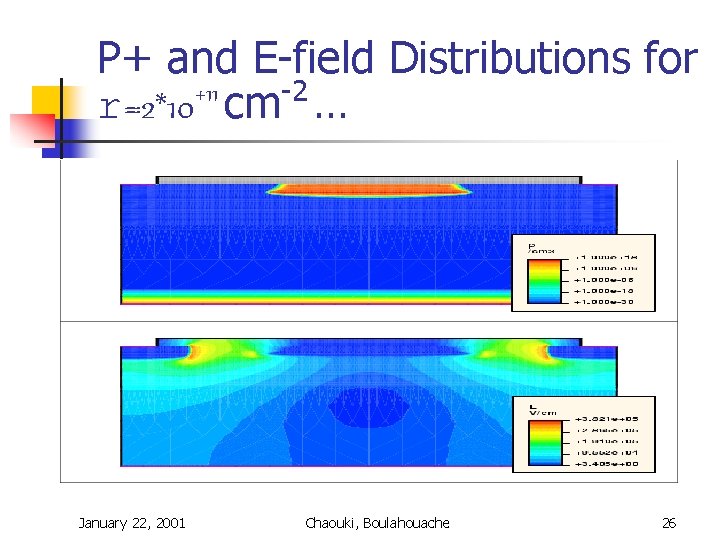
P+ and E-field Distributions for +11 -2 r=2*10 cm … January 22, 2001 Chaouki, Boulahouache 26
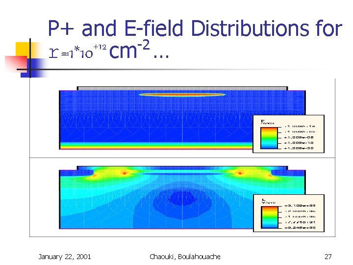
P+ and E-field Distributions for +12 -2 r=1*10 cm … January 22, 2001 Chaouki, Boulahouache 27
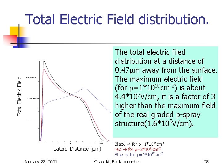
Total Electric Field distribution. Total Electric Field The total electric filed distribution at a distance of 0. 47 mm away from the surface. The maximum electric field (for r=1*1010 cm-2) is about 4. 4*105 V/cm, it is a factor of 3 higher than the maximum field of the real graded p-spray structure(1. 6*105 V/cm). Lateral Distance (mm) January 22, 2001 Black for r=1*1010 cm-2 red for r=2*1011 cm-2 Blue for r=1*1012 cm-2 Chaouki, Boulahouache 28
Conclusion… Ø Ø The oxide charge is a key element that affects the lateral field in n+/n/p+ pixel structures. P-spray detectors need to have enough p+ doping to compensate the inversion layer up to the saturation charge in the oxide, thus they start with very high lateral fields. P-stop starts with lower lateral fields, but their properties deteriorate with the increased radiation level. January 22, 2001 Chaouki, Boulahouache 29
- Slides: 29