Simulation of SEE with Sentaurus TCAD Including an

- Slides: 28

Simulation of SEE with Sentaurus TCAD Including an example on a very simple VDMOS model Pablo Fernández Martínez R 2 E/FDA Update Meeting 11 th May 2017

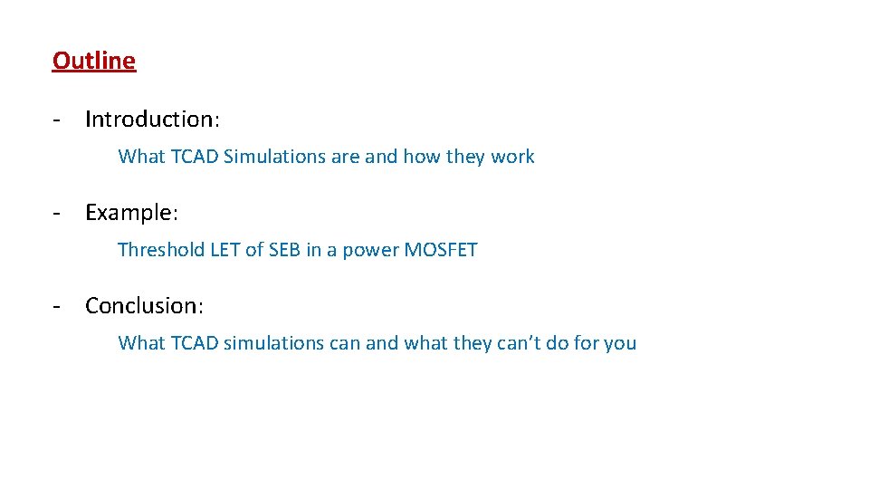
Outline - Introduction: What TCAD Simulations are and how they work - Example: Threshold LET of SEB in a power MOSFET - Conclusion: What TCAD simulations can and what they can’t do for you

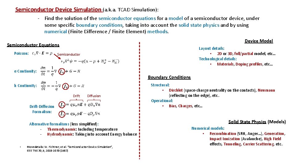
Semiconductor Device Simulation (a. k. a. TCAD Simulation): - Find the solution of the semiconductor equations for a model of a semiconductor device, under some specific boundary conditions, taking into account the solid state physics and by using numerical (Finite Difference / Finite Element) methods. Device Model Semiconductor Equations Poisson: Layout details: • 2 D or 3 D, full/partial model, etc… Technological details: • Materials, Doping profiles, etc… Semiconductor e Continuity: Boundary Conditions h Continuity: Drift-Diffusion Formalism: Diffusion Alternative formalisms (less simplified): - Thermodynamic: Including temperature - Hydrodynamic: Taking into account Energy balance • Structural: • Dirchlet (space-charge neutrality on the contacts), Neumann (reflecting on the edge), etc. . Operational: • Bias, Charges, etc… More details: W. Fichtner, et al. “Semiconductor Device Simulation”, IEEE TNS 30, 9, 1018 -1030 (1983) Solid State Physics (Models) Numerical models: • Recombination (SRH, Auger…), Generation, Impact Ionization (Avalanche), High Field effects, Tunneling, Carrier Scattering, etc. .

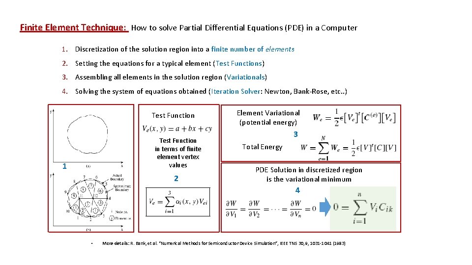
Finite Element Technique: How to solve Partial Differential Equations (PDE) in a Computer 1. Discretization of the solution region into a finite number of elements 2. Setting the equations for a typical element (Test Functions) 3. Assembling all elements in the solution region (Variationals) 4. Solving the system of equations obtained (Iteration Solver: Newton, Bank-Rose, etc. . ) Test Function in terms of finite element vertex values 1 2 Element Variational (potential energy) 3 Total Energy PDE Solution in discretized region is the variational minimum 4 • More details: R. Bank, et al. “Numerical Methods for Semiconductor Device Simulation”, IEEE TNS 30, 9, 1031 -1041 (1983)

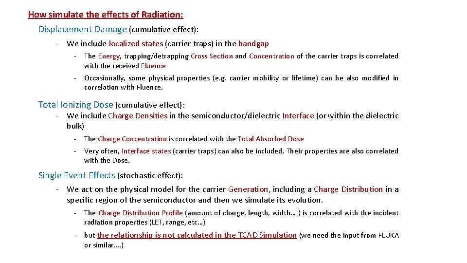
How simulate the effects of Radiation: Displacement Damage (cumulative effect): - We include localized states (carrier traps) in the bandgap - The Energy, trapping/detrapping Cross Section and Concentration of the carrier traps is correlated with the received Fluence - Occasionally, some physical properties (e. g. carrier mobility or lifetime) can be also modified in correlation with Fluence. Total Ionizing Dose (cumulative effect): - We include Charge Densities in the semiconductor/dielectric Interface (or within the dielectric bulk) - The Charge Concentration is correlated with the Total Absorbed Dose - Very often, Interface states (carrier traps) can also be included. Their properties are also correlated with the Dose. Single Event Effects (stochastic effect): - We act on the physical model for the carrier Generation, including a Charge Distribution in a specific region of the semiconductor and then we simulate its evolution. - The Charge Distribution Profile (amount of charge, length, width… ) is correlated with the incident radiation properties (LET, range, etc…) - but the relationship is not calculated in the TCAD Simulation (we need the input from FLUKA or similar…. )

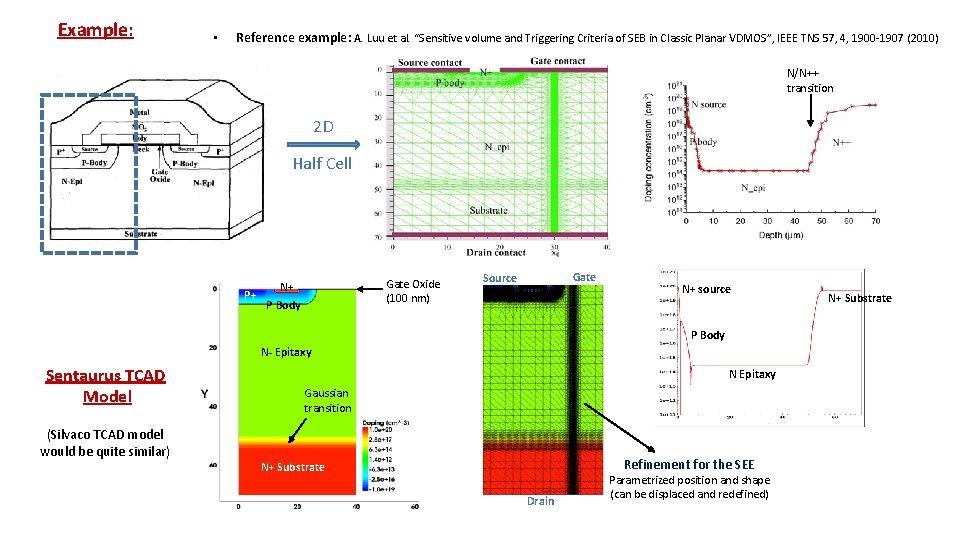
Example: • Reference example: A. Luu et al. “Sensitive volume and Triggering Criteria of SEB in Classic Planar VDMOS”, IEEE TNS 57, 4, 1900 -1907 (2010) N/N++ transition 2 D Half Cell P+ Gate Oxide (100 nm) N+ P Body Gate Source N+ source P Body N- Epitaxy Sentaurus TCAD Model (Silvaco TCAD model would be quite similar) N Epitaxy Gaussian transition Refinement for the SEE N+ Substrate Drain Parametrized position and shape (can be displaced and redefined) N+ Substrate

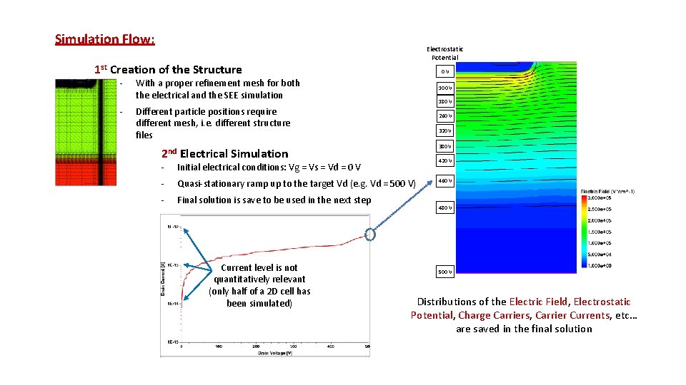
Simulation Flow: Electrostatic Potential 1 st Creation of the Structure - 0 V With a proper refinement mesh for both the electrical and the SEE simulation 100 V 180 V Different particle positions require different mesh, i. e. different structure files 2 nd 260 V 320 V 380 V Electrical Simulation 420 V - Initial electrical conditions: Vg = Vs = Vd = 0 V - Quasi-stationary ramp up to the target Vd (e. g. Vd = 500 V) - Final solution is save to be used in the next step Current level is not quantitatively relevant (only half of a 2 D cell has been simulated) 460 V 480 V 500 V Distributions of the Electric Field, Electrostatic Potential, Charge Carriers, Carrier Currents, etc… are saved in the final solution

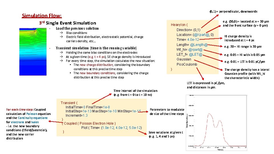
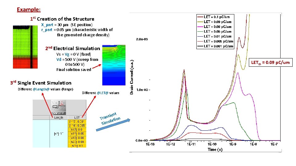
(0, 1) = perpendicular, downwards Simulation Flow: 3 rd Single Event Simulation - - Load the previous solution à Bias conditions à Electric field distribution, electrostatic potential, charge carriers density, etc… Transient simulation (time is the running variable) à Holding the same bias conditions on the electrodes à At a given time (e. g. t = 4 ps), SE charge density is introduced à For every time step, the simulation calculates the new situation: • The new charge distribution, considering the boundary conditions at this precise time step • The new boundary conditions, considering the charge distribution at this precise time step Heavy. Ion ( Direction= (0, 1) Location= (@Xpart@, 0) Time= 4. 0 e-12 Length= @Length@ Wt_hi= @rpart@ LET_f= @LET@ Gaussian Pico. Coulomb ) Time interval of the simulation (e. g. from t = 0 to t = 10 ns) For each time step: Coupled calculation of Poisson equation and the Continuity equations for electrons and holes - i. e. the new boundary conditions (Efield/potential), and the new carrier distribution Transient ( Initial. Time=0 Final. Time=1 e-8 Initial. Step=1 e-13 Max. Step=1 e-10 Min. Step=1 e-15 Increment=1. 3 ) { Coupled { Poisson Electron Hole } Plot ( Time= (1. 0 e-12; 4. 0 e-12; 5. 0 e-12) } Parameters to modulate de size of the time steps Save solutions at given t (e. g. 1, 4 and 5 ps) e. g. (30, 0) = located at x = 30 µm and the front surface (y = 0 µm) HI charge density is introduced at t = 4 ps e. g. 20 = HI range is 20 µm e. g. 0. 05 = HI with is 0. 05 µm e. g. 0. 01 = LET is 0. 01 p. C/µm The charge density has a lateral Gaussian profile (with Wt_hi the characteristic width) LET is expressed in p. C/µm, and distances in µm.

Example: 1 st Creation of the Structure X_part = 30 µm (SE position) r_part = 0. 05 µm (characteristic width of the generated charge density) 2 nd Electrical Simulation Vs = Vg = 0 V (fixed) Vd = 500 V (sweep from 0 to 500 V) Final solution saved LETth = 0. 09 p. C/um 3 rd Single Event Simulation Different @Length@ values (Range) Different @LET@ values ient s n a n Tr atio l u m Si

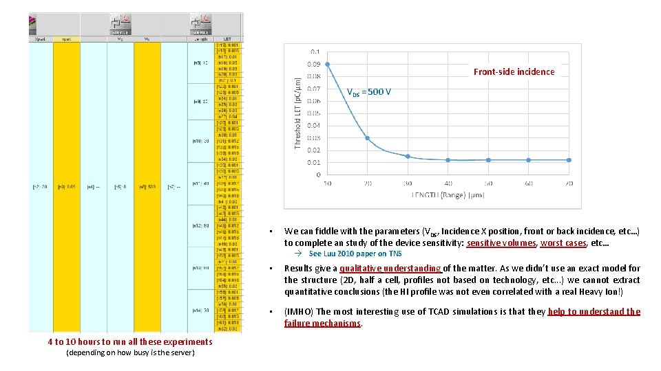
Front-side incidence VDS = 500 V • We can fiddle with the parameters (VDS, Incidence X position, front or back incidence, etc…) to complete an study of the device sensitivity: sensitive volumes, worst cases, etc… à See Luu 2010 paper on TNS 4 to 10 hours to run all these experiments (depending on how busy is the server) • Results give a qualitative understanding of the matter. As we didn’t use an exact model for the structure (2 D, half a cell, profiles not based on technology, etc. . . ) we cannot extract quantitative conclusions (the HI profile was not even correlated with a real Heavy Ion!) • (IMHO) The most interesting use of TCAD simulations is that they help to understand the failure mechanisms.

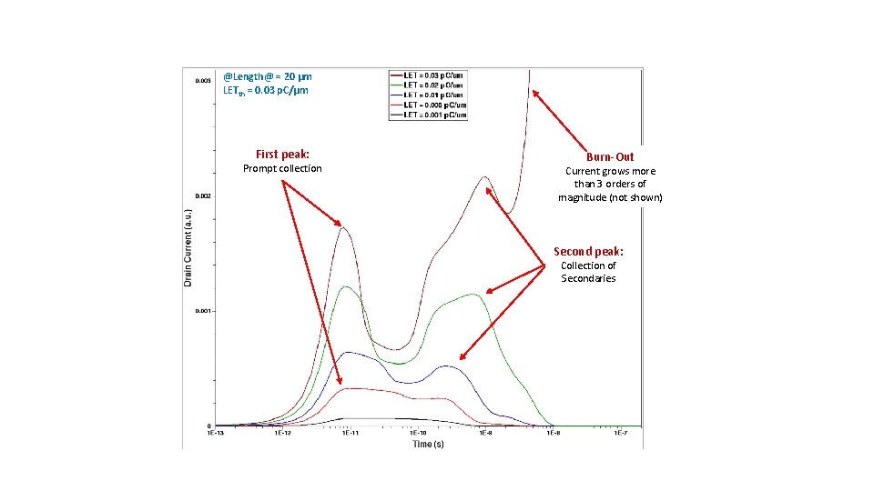
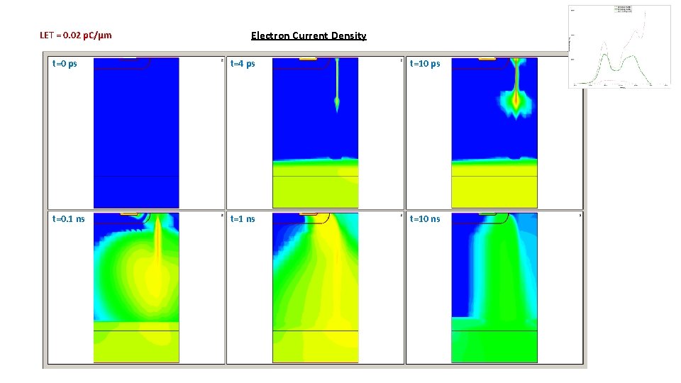
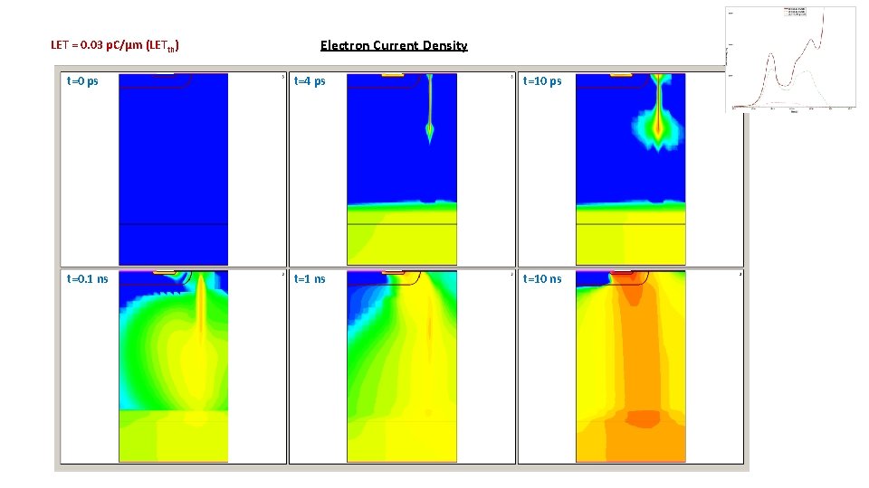
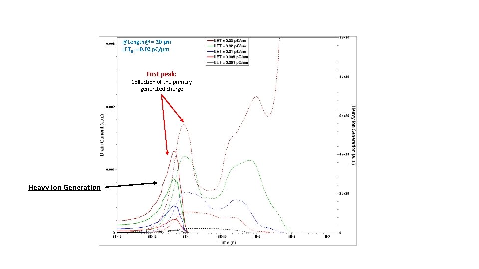
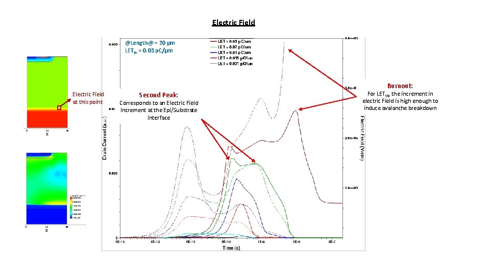
@Length@ = 20 µm LETth = 0. 03 p. C/µm First peak: Prompt collection Burn-Out Current grows more than 3 orders of magnitude (not shown) Second peak: Collection of Secondaries

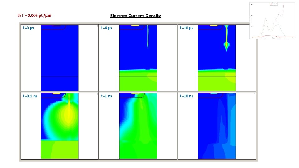
LET = 0. 005 p. C/µm Electron Current Density t=0 ps t=4 ps t=10 ps t=0. 1 ns t=10 ns

LET = 0. 02 p. C/µm Electron Current Density t=0 ps t=4 ps t=10 ps t=0. 1 ns t=10 ns

LET = 0. 03 p. C/µm (LETth) Electron Current Density t=0 ps t=4 ps t=10 ps t=0. 1 ns t=10 ns

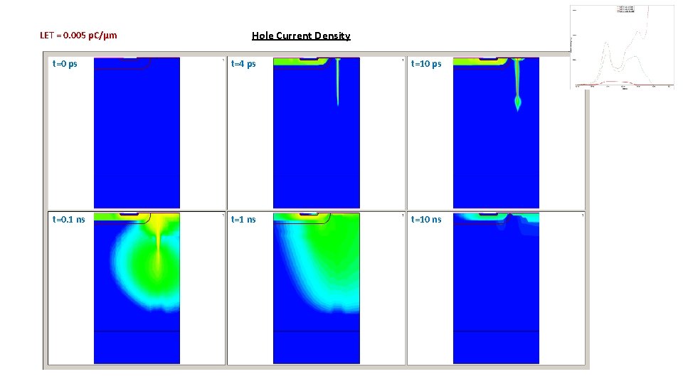
LET = 0. 005 p. C/µm Hole Current Density t=0 ps t=4 ps t=10 ps t=0. 1 ns t=10 ns

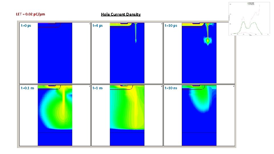
LET = 0. 02 p. C/µm Hole Current Density t=0 ps t=4 ps t=10 ps t=0. 1 ns t=10 ns

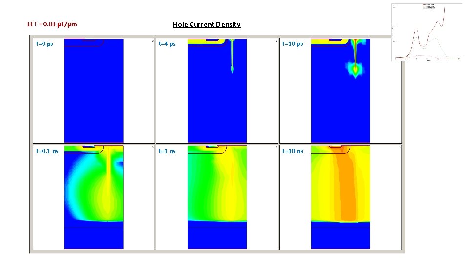
LET = 0. 03 p. C/µm Hole Current Density t=0 ps t=4 ps t=10 ps t=0. 1 ns t=10 ns

@Length@ = 20 µm LETth = 0. 03 p. C/µm First peak: Collection of the primary generated charge Heavy Ion Generation

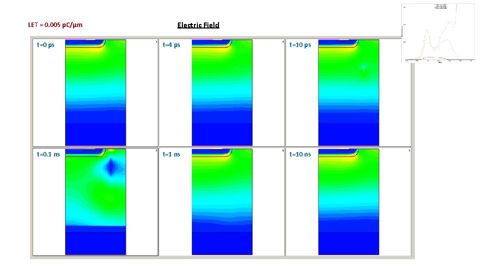
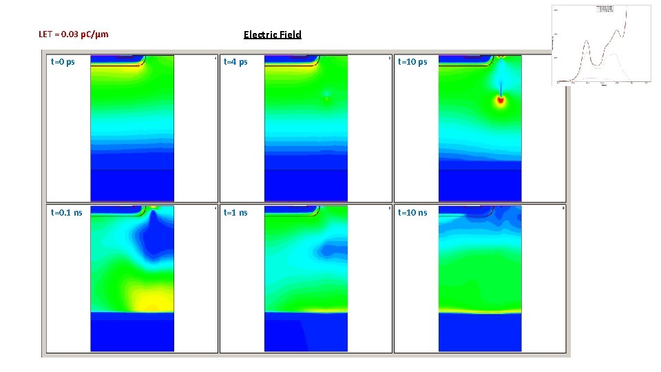
LET = 0. 005 p. C/µm Electric Field t=0 ps t=4 ps t=10 ps t=0. 1 ns t=10 ns

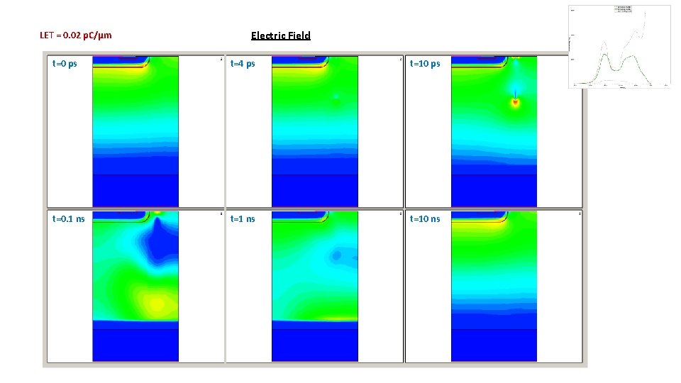
LET = 0. 02 p. C/µm Electric Field t=0 ps t=4 ps t=10 ps t=0. 1 ns t=10 ns

LET = 0. 03 p. C/µm Electric Field t=0 ps t=4 ps t=10 ps t=0. 1 ns t=10 ns

Electric Field @Length@ = 20 µm LETth = 0. 03 p. C/µm Burnout: Electric Field at this point Second Peak: Corresponds to an Electric Field increment at the Epi/Substrate interface For LETth, the increment in electric Field is high enough to induce avalanche breakdown

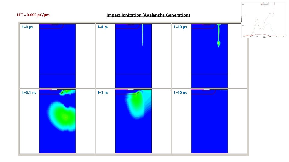
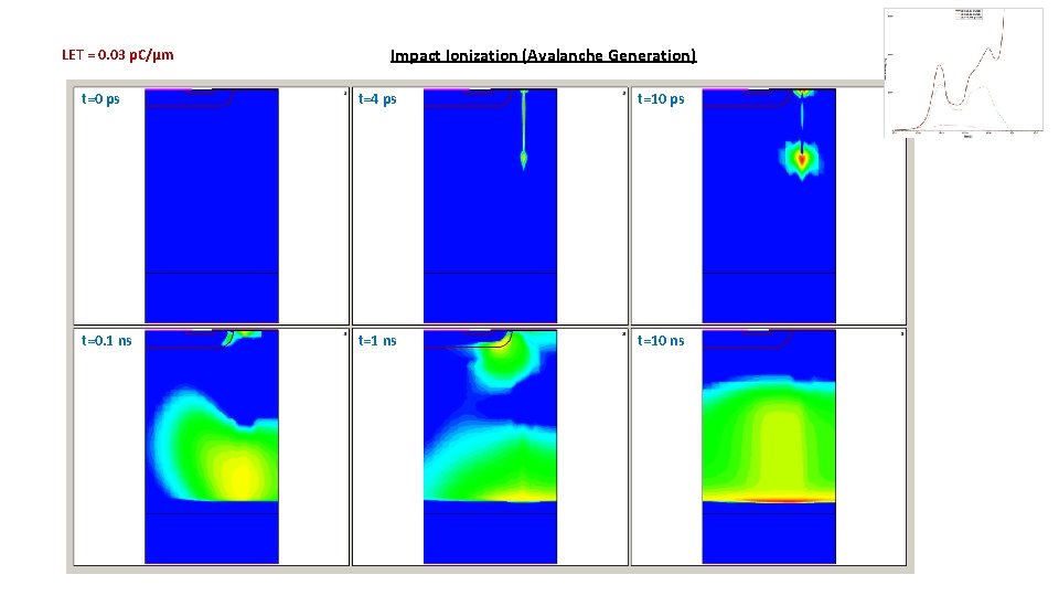
LET = 0. 005 p. C/µm Impact Ionization (Avalanche Generation) t=0 ps t=4 ps t=10 ps t=0. 1 ns t=10 ns

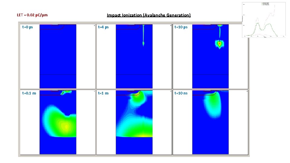
LET = 0. 02 p. C/µm Impact Ionization (Avalanche Generation) t=0 ps t=4 ps t=10 ps t=0. 1 ns t=10 ns

LET = 0. 03 p. C/µm Impact Ionization (Avalanche Generation) t=0 ps t=4 ps t=10 ps t=0. 1 ns t=10 ns

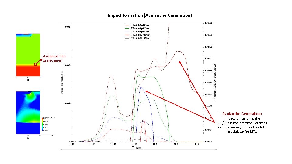
Impact Ionization (Avalanche Generation) Avalanche Gen. at this point Avalanche Generation: Impact Ionization at the Epi/Substrate interface increases with increasing LET, and leads to breakdown for LETth

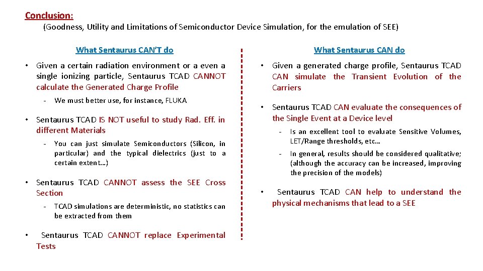
Conclusion: (Goodness, Utility and Limitations of Semiconductor Device Simulation, for the emulation of SEE) What Sentaurus CAN’T do What Sentaurus CAN do • Given a certain radiation environment or a even a single ionizing particle, Sentaurus TCAD CANNOT calculate the Generated Charge Profile • Given a generated charge profile, Sentaurus TCAD CAN simulate the Transient Evolution of the Carriers - We must better use, for instance, FLUKA • Sentaurus TCAD IS NOT useful to study Rad. Eff. in different Materials - You can just simulate Semiconductors (Silicon, in particular) and the typical dielectrics (just to a certain extent…) • Sentaurus TCAD CANNOT assess the SEE Cross Section - TCAD simulations are deterministic, no statistics can be extracted from them • Sentaurus TCAD CANNOT replace Experimental Tests • Sentaurus TCAD CAN evaluate the consequences of the Single Event at a Device level - Is an excellent tool to evaluate Sensitive Volumes, LET/Range thresholds, etc… - In general, results should be considered qualitative; (although the accuracy can be increased, improving the precision of the models) • Sentaurus TCAD CAN help to understand the physical mechanisms that lead to a SEE

¡Muchas Gracias!