Simplified Transceiver Architecture Transceiver Role of a Transmitter


")


 A wc D 0 Saturates the following stages capacitive coupling substrate")
 level + DC Offset t -")


 vi(t) A I D Q 0")


")


 DSP A/D Phase and")


 Complex Bandpass Filter I Q LO 1 I Q LO")
 I Q LO 1 Q I LO 2 Both schemes")
 • Use I/Q")


- Slides: 83
Simplified Transceiver Architecture
Transceiver Role of a Transmitter Information 2. add data to carrier 3. shift to high frequency Modulator A 0 90 u. P/ DSP A Q Data D Oscillator bias 1. create carrier The lkhefw wlkhq wejklh wajkhrqwilu wilehr esjlkh qwh wlh wae. wklhjr qlih qilh q q 3 wih lihewrw wejklh wajkhrqwilu q esjlkh qwh wlh wae. lihewrw wklhjr qlih qilh q q 3 wih wejklh wajkhrqwilu q wae. esjlkh qwh wlh wklhjr qlih qilh q q 3 wih lihewrw q wklhjr qlih qilh q q 3 wih q wejklh wajkhrqwilu esjlkh wae. qwh wlh wklhjr qlih qilh q q 3 wih lihewrw wejklh wajkhrqwilu q esjlkh qwh wlh wae. wklhjr qlih qilh q q 3 wih lihewrw wklhjr qlih qilh q q 3 wih q wejklh wajkhrqwilu q wae. esjlkh qwh wlh wklhjr qlih qilh q q 3 wih lihewrw wejklh wajkhrqwilu q wae. I Data Power Amplifier 4. amplify to broadcast The lkhefw wlkhq wejklh wajkhrqwilu wilehr esjlkh qwh wlh wae. wklhjr qlih qilh q q 3 wih lihewrw wejklh wajkhrqwilu q esjlkh qwh wlh wae. lihewrw wklhjr qlih qilh q q 3 wih wejklh wajkhrqwilu q wae. esjlkh qwh wlh wklhjr qlih qilh q q 3 wih lihewrw wejklh wajkhrqwilu q esjlkh qwh wlh wae. lihewrw wklhjr qlih qilh q q 3 wih q wklhjr qlih qilh q q 3 wih wejklh wajkhrqwilu q esjlkh qwh wlh wae. wklhjr qlih qilh q q 3 wih lihewrw wejklh wajkhrqwilu q esjlkh qwh wlh wae. lihewrw wklhjr qlih qilh q q 3 wih q wejklh wajkhrqwilu q esjlkh qwh wlh wae. lihewrw D Mixer Antenna HPMX-2007 The lkhefw wlkhq wejklh wajkhrqwilu wilehr esjlkh qwh wlh wae. wklhjr qlih qilh q q 3 wih lihewrw wejklh wajkhrqwilu q wae. esjlkh qwh wlh wklhjr qlih qilh q q 3 wih lihewrw q wejklh wajkhrqwilu esjlkh qwh wlh wae. wklhjr qlih qilh q q 3 wih lihewrw wejklh wajkhrqwilu q esjlkh qwh wlh wae. wklhjr qlih qilh q q 3 wih lihewrw q wklhjr qlih qilh q q 3 wih wejklh wajkhrqwilu q esjlkh qwh wlh wae. wklhjr qlih qilh q q 3 wih lihewrw wejklh wajkhrqwilu q wae. esjlkh qwh wlh wklhjr qlih qilh q q 3 wih lihewrw q Power Supply Baseband Processor
Role of a Receiver Information 4. discard carrier and recover data 2. shift to lower frequency (cost and/or performance) De-Modulator A HPMX-2007 The lkhefw wlkhq wejklh wajkhrqwilu wilehr esjlkh qwh wlh wae. wklhjr qlih qilh q q 3 wih lihewrw wejklh wajkhrqwilu q wae. esjlkh qwh wlh wklhjr qlih qilh q q 3 wih lihewrw q wejklh wajkhrqwilu esjlkh wae. qwh wlh wklhjr qlih qilh q q 3 wih lihewrw wejklh wajkhrqwilu q esjlkh qwh wlh wae. wklhjr qlih qilh q q 3 wih lihewrw q wklhjr qlih qilh q q 3 wih wejklh wajkhrqwilu q esjlkh qwh wlh wae. wklhjr qlih qilh q q 3 wih lihewrw wejklh wajkhrqwilu q wae. esjlkh qwh wlh wklhjr qlih qilh q q 3 wih lihewrw q 0 I Data u. P/ DSP 90 Antenna Low Noise Amplifier 1. amplify received signal with min. added noise A Q Data D Oscillator bias 3. LO for down conversion Power Supply The lkhefw wlkhq wejklh wajkhrqwilu wilehr esjlkh qwh wlh wae. wklhjr qlih qilh q q 3 wih lihewrw wejklh wajkhrqwilu q esjlkh qwh wlh wae. lihewrw wklhjr qlih qilh q q 3 wih wejklh wajkhrqwilu q wae. esjlkh qwh wlh wklhjr qlih qilh q q 3 wih lihewrw q wklhjr qlih qilh q q 3 wih q wejklh wajkhrqwilu esjlkh qwh wlh wae. wklhjr qlih qilh q q 3 wih lihewrw wejklh wajkhrqwilu q esjlkh qwh wlh wae. wklhjr qlih qilh q q 3 wih lihewrw wklhjr qlih qilh q q 3 wih q wejklh wajkhrqwilu q wae. esjlkh qwh wlh wklhjr qlih qilh q q 3 wih lihewrw wejklh wajkhrqwilu q wae. Baseband Processor D Mixer The lkhefw wlkhq wejklh wajkhrqwilu wilehr esjlkh qwh wlh wae. wklhjr qlih qilh q q 3 wih lihewrw wejklh wajkhrqwilu q esjlkh qwh wlh wae. lihewrw wklhjr qlih qilh q q 3 wih wejklh wajkhrqwilu q wae. esjlkh qwh wlh wklhjr qlih qilh q q 3 wih lihewrw wejklh wajkhrqwilu q esjlkh qwh wlh wae. lihewrw wklhjr qlih qilh q q 3 wih q wklhjr qlih qilh q q 3 wih wejklh wajkhrqwilu q esjlkh qwh wlh wae. wklhjr qlih qilh q q 3 wih lihewrw wejklh wajkhrqwilu q esjlkh qwh wlh wae. lihewrw wklhjr qlih qilh q q 3 wih q wejklh wajkhrqwilu q esjlkh qwh wlh wae. lihewrw bias
Mixer = Multiplying up/down conversion • Frequency translation device • Ideal mixer: AB A B – Doesn’t “mix”; it multiplies
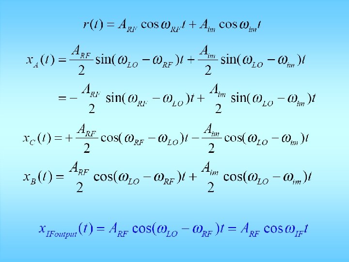
Image problem converting to IF A has desired signal at w. IF A 1 cos(w. RFt) plus an interference at w. IM A 2 cos(w. IMt) B is at w. LO And: w. RF - w. LO = w. LO - w. IM = w. IF Both converted to IF, Can’t be cleaned once corrupted
Image Problem
Problem of Image Signal
Problem of Image Signal • Solution: Image Rejection Filter
Problem of Half IF • Second order harmonic
Superheterodyne Receiver
Multi IF Stage Receivers • Received RF signal is down converted stage by stage until the desired final IF is obtained • Frequency conversion ratio of each stage is usually kept lower than 10. – For example, RF 1800 MHz IF 1 450 MHz, then IF 2 90 MHz, and finally IF 3 18 MHz. – Corresponding ratios are: 4; 5; 5; total 100. • Each stage has it’s own image problem • Each stage requires demanding filtering – Typically done off chip or using SAW – Complicated, bulky, expensive
IF and LO frequency selection • Fixed RF filter before LNA for band selection – One for each standard – Off-chip, high quality, no freedom • IF frequency is selected at design – Fixed for each product • LO frequency is tuned in real time – |RF–LO|=IF – Actual RF freq depends on which channel is assigned to device – LO tuning range must cover RF bandwidth
Superheterodyne Receiver(cont. )
Selection of IF • If IF is large, – better separation between RF and image – better image rejection – easier image rejection filter design – More stages of down conversion • Other IF selection criteria – Select IF so that image freq is outside of RF band – IF >= (RF BW)/2 • Sometime may not be possible, if (RF BW)/2 is within RF Band
• For each channel assignment, there are two choices of LO freq that meets the requirement |RF–LO|=IF. • Q: should LO > RF, or LO < RF? ?
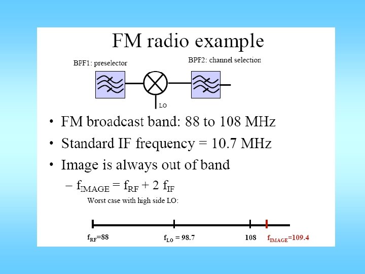
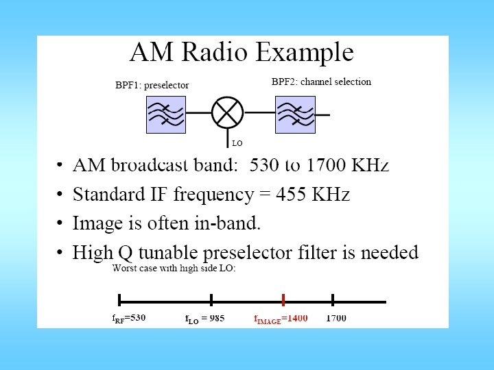
Example: AM Radio • • • AM radio band: 530 to 1610 KHz BW/2 = (1610 -530)/2=1080/2=540, in band IF has to be lower. Commonly: 455 k. Hz Image can be in AM band If LO is on low side, LO tuning range is: – (530 to 1610) – 455 = (75 to 1155) – LO lowest to highest is a factor of 15. 4 • If LO is on high side, LO tuning range is: – (530 to 1610) + 455 = (985 to 2065) – LO lowest to highest is a factor of 2. 01
Direct Conversion Receiver No image problem
Direct Conversion Receiver LO is at same frequency as RF 1/f noise here can end up in channel Self mixing cause DC problem + Eliminate IF SAW, IF PLL and image filtering + Integration + Avoids image problem - Quadrature RF down conversion required - DC problem - Typically requires offset or 2 x LO to avoid coupling
DC Offset (Self-mixing) A wc D 0 Saturates the following stages capacitive coupling substrate coupling bondwire coupling wc a. LO(t)=ALOcos(w c+q) A wc wc D 0
DC Offset (Self-mixing) level + DC Offset t -
DC Offset Cancellation • Capacitive Coupling – Requires a large capacitor • Negative Feedback – Nonlinear • TDMA Offset Cancellation – Requires a large capacitor -A
1/f noise effect • CMOS transistors has significant 1/f noise at low to DC frequency • Significantly noise performance of direct conversion receivers 1/f noise Receive signal f
Even-Order Distortion Direct feed through
Mirror Signal • Upper sideband lower sideband are identical
Mirror Signal • Upper sideband lower sideband are not identical
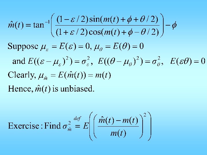
Mirror Signal Suppression • Quadrature Down Conversion ui(t) vi(t) A I D Q 0 D 90 a(t) A uq(t) vq(t)
Quadrature Conversion
Quadrature Down Conversion
I/Q Mismatch Phase & Gain Error I 0 90 Phase & Gain Error a(t) Q Phase & Gain Error
I/Q Mismatch due to LO errors
Effect of gain mismatch Gain error Effect of phase mismatch Phase error
Use of I/Q down conversion recovers the nonsymmetrical receive signal spectrum But port isolation becomes more challenging Selfmixing and even order distortion may affect both channels and affect each other, causing additional I/Q mismatch
DC and 1/f cancellation A/D 0 Base Band 90 a(t) DSP A/D Phase and gain mismatch compensation
Summary of Direct Conversion Receiver • No need for imager reject filter • Suitable for monolithic integration with baseband • DC offsets due to crosstalk of input ports of mixer • Even order IM direct feed through to baseband • Quadrature down conversion suppresses mirror • I/Q mismatch due to mismatches in parasitics • Low power consumption attributes to less hardware
Low IF receiver + Eliminate IF SAW, IF PLL and image filtering + Integration + Relaxes image rejection requirements + Avoids DC problems, relaxes 1/f noise problem - Quadrature RF down conversion required - Require higher performance ADC -Additional mixer -Slower RF PLL settling -Even order distortion still problem -Low freq IF filters require large chip area
Low-IF Down Conversion Complex BPF Mirror signal, needs removal
Mirror Signal Suppression (1) Complex Bandpass Filter I Q LO 1 I Q LO 2
Mirror Signal Suppression (2) I Q LO 1 Q I LO 2 Both schemes used in heterodyne receivers for image rejection Mathematical analysis very similar
Image rejection architectures • Use additional hardware (LO’s, mixers, and filters) • Use I/Q channels which process + or – frequencies differently • Two steps of I/Q to solve both image and mirror problems • Effects limited by I/Q channel/filter matching accuracies
Image Reject Receiver • Hartley Architecture A C -90° 0 90 RF input w LO B IF output
Hartley Architecture xcos xsin
IQ error effect • Ideal IQ: image completely rejected • If signal and image not single tone, 90 o shift is not exact • Local oscillator’s sine and cosine not matched in magnitude and phase • 90 o phase shifter may have both gain and phase error • All lead to incomplete image rejection
IPR Evaluation and IRR – LO error
Input image power ratio
Image Reject Receiver Hartley Architecture with simple 90 deg phase shiftor
Gain Mismatch due to R, C errors At w = 1/RC:
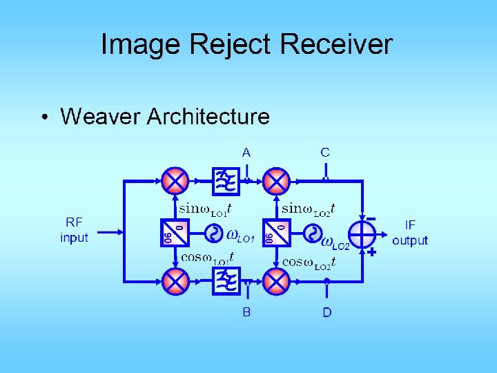
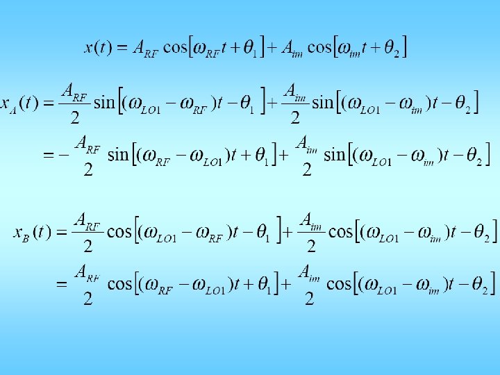
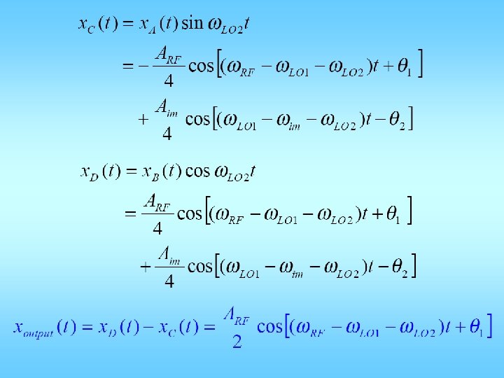
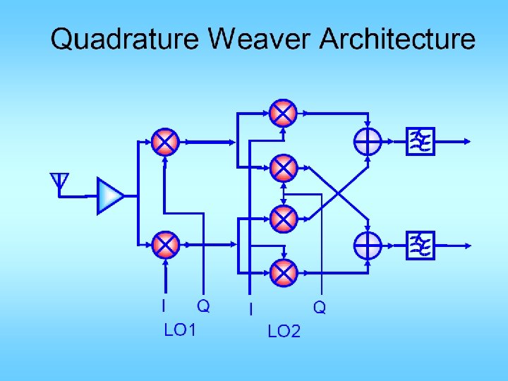
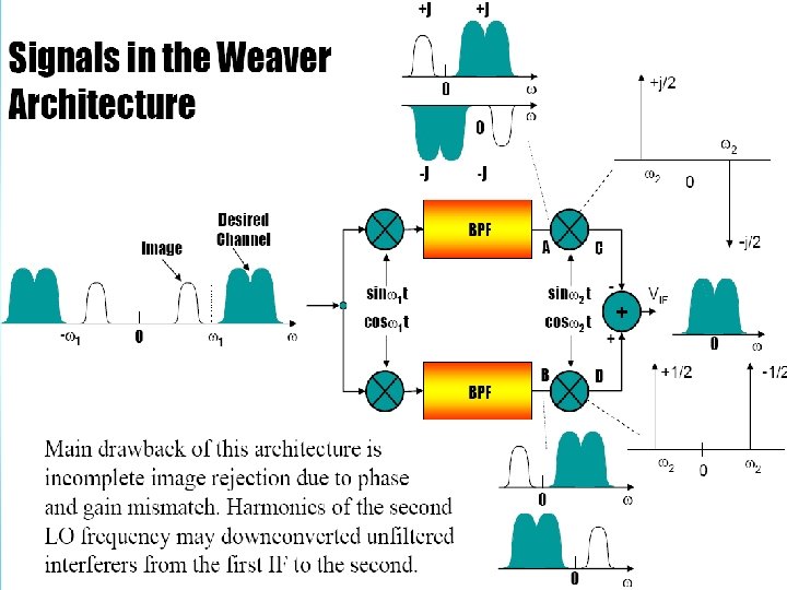
Weaver Architecture
Weaver Architecture
Digital IF? • To avoid 0 -IF or low-IF issues, IF frequencies can’t be too low • Recall: RF-IF ratio within 10 • Typical RF freq is in 1 to 5 GHz, IF needs to be more than 100 to 500 MHz • But dynamic range requirements requires >= 14 bit resolution • No such ADC’s are available • But signal bandwidth much smaller, • Subsampling Receivers
• Example: 1. 8 GHz GSM Specifications: IF carrier frequency = 246 MHz, Channel BW = 200 KHz, Input Dynamic Range = 90 d. B. ü ü x x 2 digital low frequency mixers, no noise and distortion. Easier I&Q matching. No DC offset and 1/f noise. More digital means easier integration on a CMOS process. SNR degradation due to noise folding ADC & SH have to run at high clock to minimize noise folding.
Noise folding problem White noise 0 IF …… fs 2 fs …… 0 IF Baseband noise increased by IF/fs factor
• The aliased noise, once happened, cannot be removed in the digital domain • Band pass filtering of IF before sampling can reduce the noise in lower frequency – Requires expensive IF filters – Against the spirit of moving more things to digital • Reduce IF frequency and increase fs frequency so that IF/fs ratio is not large – More stringent requirement on RF filtering and image rejection – Requires faster ADC
Example UMTS/DCS 1800 Specifications Frequency Band Channel BW System Sensitivity BER Blocking Characteristics Adjacent Channel Interference DCS 1800 1805 - 1880 MHz 200 k. Hz -102 d. Bm 1 e-3 600 - 800 k. Hz: -43 d. Bm 800 - 1600 k. Hz: -43 d. Bm 1600 - 3000 k. Hz: -33 d. Bm > 3000 k. Hz: -26 d. Bm Cochannel: -9 d. Bc 200 k. Hz: 9 d. Bc 400 k. Hz: 41 d. Bc 600 k. Hz: 49 d. Bc UMTS 2110 - 2170 MHz 5 MHz -117 d. Bm(@32 ksps) 1 e-3 10 - 15 MHz: -56 d. Bm 15 - 60 MHz: -44 d. Bm 60 - 85 MHz: -30 d. Bm > 85 MHz: -15 d. Bm 5 MHz: -52 d. Bm
Sensitivity • Adjacent Channel Interference Adjacent Channel • Co-Channel Interference 890. 4 Adjacent Channel 890. 4 Desired Channel 890. 4 890. 6 MHz 890. 4
Multi-Channel, Multi-Mode Dynamic Range, DCS 1800
Multi-Channel, Multi-Mode Dynamic Range, DCS 1800 PB = 13 d. Bm, Px = -60 d. Bm PB: Px = 73 d. B If want FS: 1 LSB > 73 d. B >12 bit resolution If want digital channel selection + filtering, fs >= 2 BW fs >= 150 MHz If want noise floor 20 d. B below wanted signal SFDR >= 13 – (-60) + 20 = 93 d. B Type of ADC needed: 150 MSPS, 13 -14 bit, 95 -100 d. B SFDR
Sensitivity Desired Signal Receiver Added Noise Receiver Thermal Noise
Sensitivity Power to Antenna: +40 d. Bm TX. Antenna Gain: +10 d. B Frequency: 10 GHz Bandwidth: 100 MHz Rcvr. Antenna Gain: +60 d. B Transmitter: ERP Path Losses Rcvr. Ant. Gain + 50 d. Bm -200 d. B 60 d. B Power to Receiver -80 d. Bm Receiver: Noise Floor @ 290 K Noise in 100 MHz BW Receiver N. F. ERP = +50 d. Bm Path Losses: 200 d. B Receiver Sensitivity - 174 d. Bm/Hz Margin: 4 d. B + 80 d. B +10 d. B -84 d. Bm How to increase Margin by 3 d. B ?
Selectivity IF Filter RF Filter Ch Ch Ch 1 2 3 f. RF Ch Ch Ch 1 2 3 Ch n f. IF freq f. LO freq Ch n freq
Selectivity • IF filter rejection at the adjacent channel • LO spurious in IF bandwidth • Phase noise of LO RF Filter IF Filter Receiver Added Noise Receiver Thermal Noise
Noise Figure Calculation RF input Baseban d receiver
Es/No or Eb/No=? 17!
IP 3 Calculation
Image Rejection Calculation PImage IRrequired Pdesired SNRmin f. IF f. LO (all in d. B’s) f. RF
Transmitter Architecture • Direct Conversion Transmitter • Two-step Conversion Transmitter • Offset PLL Transmitter
Transmit Specifications • Transmit spectrum mask
Receiver Specifications alternate adjacent channel Adjacent channel 20 40
Direct-conversion transmitter I 0 90 Q w. LO Pros: less spurious synthesized Cons: more LO pulling
• Direct-conversion transmitter with offset LO I 0 w 2 90 w. LO w 1 Q Pros: less LO pulling Cons: more spurious synthesized
• Two-step transmitter I 0 90 Q cosw 1 t cosw 2 t w 1 + w 2 Pros: less LO pulling superior IQ matching Cons: required high-Q bandpass filter
• Offset PLL transmitter I 0 90 Q cosw 1 t PD/LPF VCO 1/N
Weaver Architecture
Wideband IF Architecture