Simple ADC structures 1 Some ADC generates internal

- Slides: 16

Simple ADC structures 1

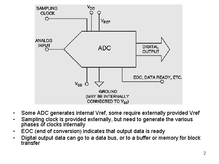
• • Some ADC generates internal Vref, some require externally provided Vref Sampling clock is provided externally, but need to generate the various phases of clocks internally EOC (end of conversion) indicates that output data is ready Digital output data can go to a data bus, or to a buffer or memory for block transfer 2

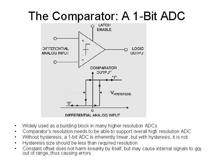
The Comparator: A 1 -Bit ADC • • • Widely used as a building block in many higher resolution ADCs Comparator’s resolution needs to be able to support overall high resolution ADC Without hysteresis, a 1 -bit ADC is inherently linear, but with hysteresis, it is not Hysteresis size should be less than required resolution Constant offset does not harm linearity by itself, but may cause internal signals to go 3 out of range, thus causing errors

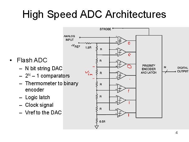
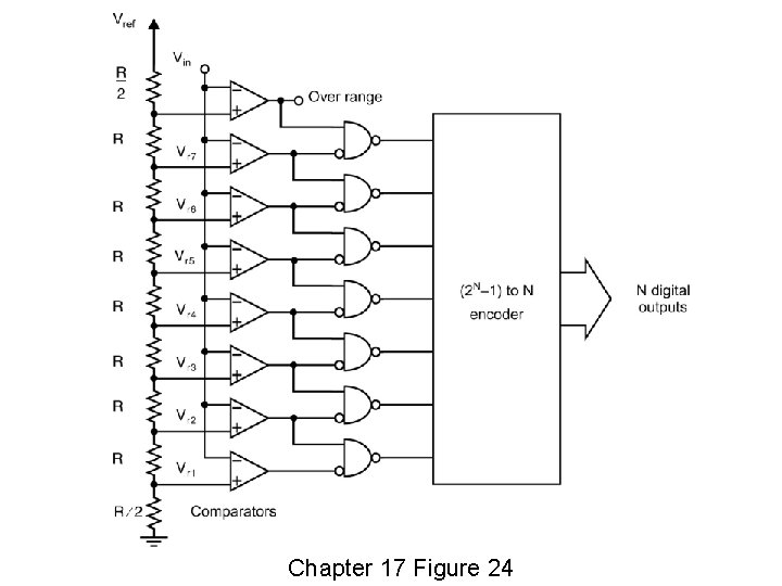
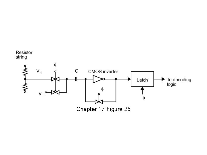
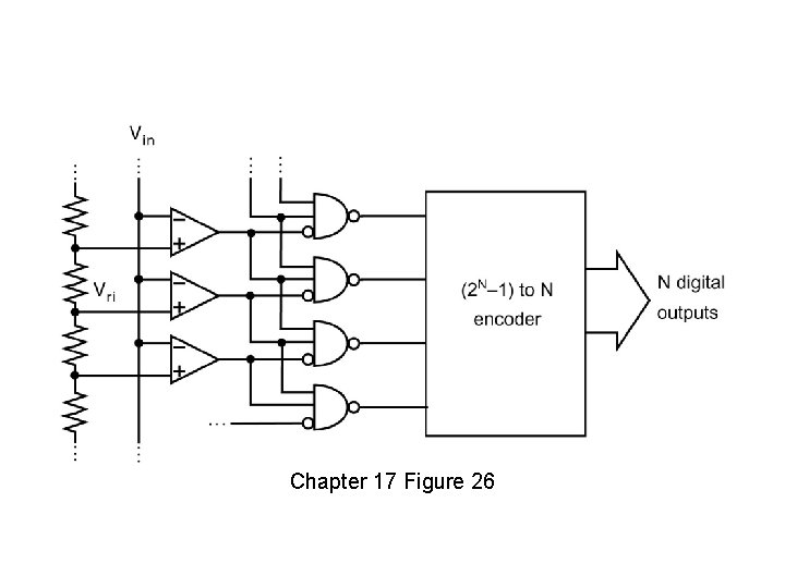
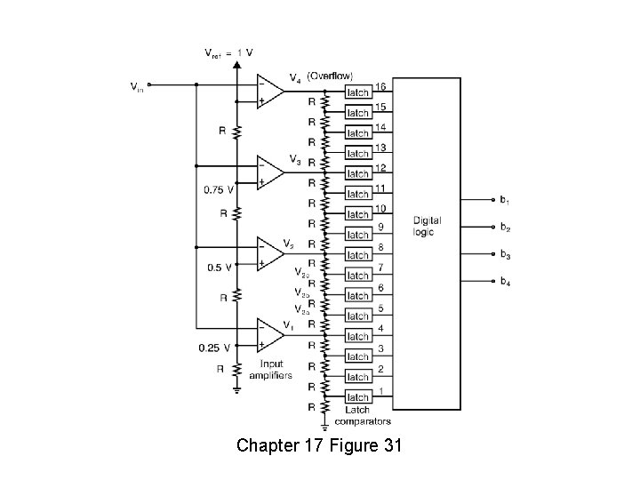
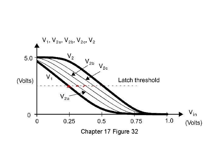
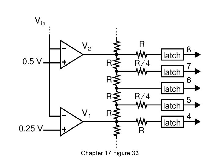
High Speed ADC Architectures • Flash ADC – N bit string DAC – 2 N – 1 comparators – Thermometer to binary encoder – Logic latch – Clock signal – Vref to the DAC 4

Chapter 17 Figure 24

Chapter 17 Figure 25

Chapter 17 Figure 26

Chapter 17 Figure 31

Chapter 17 Figure 32

Chapter 17 Figure 33

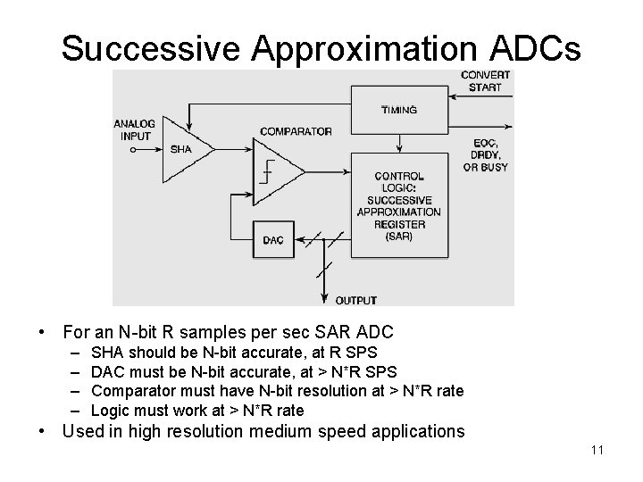
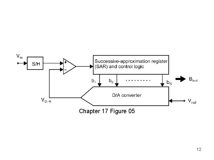
Successive Approximation ADCs • For an N-bit R samples per sec SAR ADC – – SHA should be N-bit accurate, at R SPS DAC must be N-bit accurate, at > N*R SPS Comparator must have N-bit resolution at > N*R rate Logic must work at > N*R rate • Used in high resolution medium speed applications 11

Chapter 17 Figure 05 12

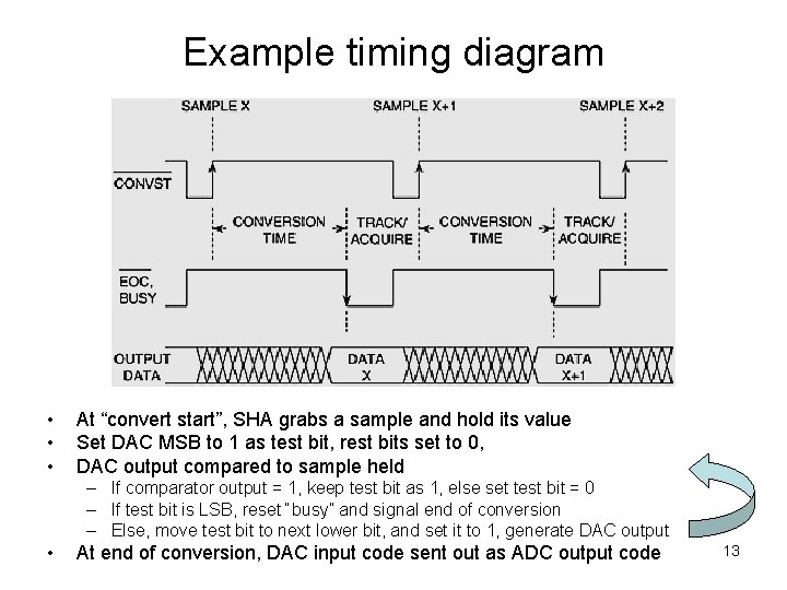
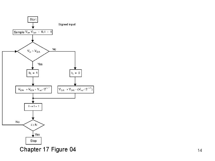
Example timing diagram • • • At “convert start”, SHA grabs a sample and hold its value Set DAC MSB to 1 as test bit, rest bits set to 0, DAC output compared to sample held – If comparator output = 1, keep test bit as 1, else set test bit = 0 – If test bit is LSB, reset “busy” and signal end of conversion – Else, move test bit to next lower bit, and set it to 1, generate DAC output • At end of conversion, DAC input code sent out as ADC output code 13

Chapter 17 Figure 04 14

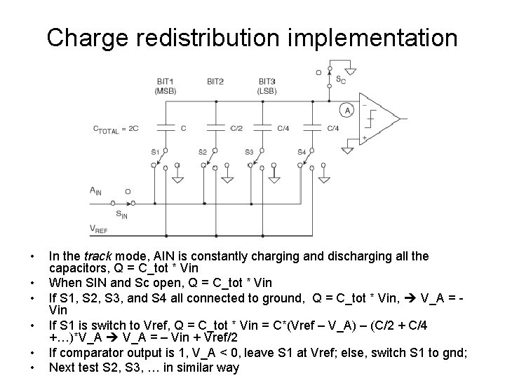
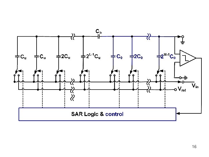
Charge redistribution implementation • • • In the track mode, AIN is constantly charging and discharging all the capacitors, Q = C_tot * Vin When SIN and Sc open, Q = C_tot * Vin If S 1, S 2, S 3, and S 4 all connected to ground, Q = C_tot * Vin, V_A = Vin If S 1 is switch to Vref, Q = C_tot * Vin = C*(Vref – V_A) – (C/2 + C/4 +…)*V_A = – Vin + Vref/2 If comparator output is 1, V_A < 0, leave S 1 at Vref; else, switch S 1 to gnd; 15 Next test S 2, S 3, … in similar way

16