
Simon Christie Hartmut F W Sadrozinski SMPL Oct
- Slides: 12
Simon Christie, Hartmut F. -W. Sadrozinski, "SMPL ", Oct 2018 First Test Results from HPK HGTD Sensors EXX 28782 -W#9 & W#10 (for ATLAS) S 10938 -6093 Type-1 • List 1
Simon Christie, Hartmut F. -W. Sadrozinski, "SMPL ", Oct 2018 Information re HPK HGTD Sensors From Ardavan Ghassemi (HPK US) Oct 19, 2018 (S 10938 -6093 is also called EXX 28782) 1. S 10938 -6093 Type-1 - Our top candidate –received 2 wafer’s of this type but w/o UBM and backside metal patter HPK-SMPL wafer 9 and 10. - Physical thickness : 200 umt - Active thickness : 35 umt - Wafer material : Same as the Sample B shipped in 2017. 2. S 10938 -6093 Type-2 - Physical thickness : 200 umt - Active thickness : 35 umt - Wafer material : Same as the Sample B shipped in 2017. 3. S 10938 -6093 Type-3 - Physical thickness : 200 umt - Active thickness : 50 umt - Wafer material : Same as the Sample A shipped in 2016. <Shipping schedule> - S 10938 -6093 Type-1, 5 wafer's : mid-Nov. - S 10938 -6093 Type-2, 5 wafer's : late Nov. - S 10938 -6093 Type-3, 5 wafer's : late Nov. If you can accept Types 2 and 3 above without UBM, Hamamatsu Japan will be able to ship them in early November. Please let me know how you’d like to proceed in this regard 2
Simon Christie, Hartmut F. -W. Sadrozinski, "SMPL ", Oct 2018 Information re HPK HGTD Sensors From Ardavan Ghassemi (HPK US) Oct 22, 2018 HPK will split the shipping of Type-2 and Type-3: -> ship two wafer each of Type-2 and Type-3 without UBM early November -> ship the rest of Type-2 and Type-3 wafers including UBM late November BTW: All wafers will have the backside metal pattern. 3
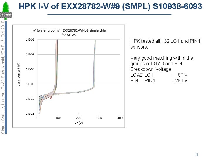
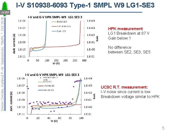
Simon Christie, Hartmut F. -W. Sadrozinski, "SMPL ", Oct 2018 HPK I-V of EXX 28782 -W#9 (SMPL) S 10938 -6093 HPK tested all 132 LG 1 and PIN 1 sensors. Very good matching within the groups of LGAD and PIN Breakdown Voltage LGAD LG 1 : 87 V PIN 1 : 280 V 4
Simon Christie, Hartmut F. -W. Sadrozinski, "SMPL ", Oct 2018 I-V S 10938 -6093 Type-1 SMPL W 9 LG 1 -SE 3 HPK measurement LG 1 Breakdown at 87 V Gain below 1 No difference between SE 2, SE 3, SE 5 UCSC R. T. measurement: I-V noise since current is low Breakdown voltage similar to HPK 5
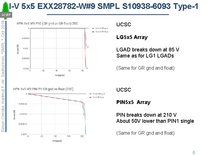
Simon Christie, Hartmut F. -W. Sadrozinski, "SMPL ", Oct 2018 I-V 5 x 5 EXX 28782 -W#9 SMPL S 10938 -6093 Type-1 UCSC LG 5 x 5 Array LGAD breaks down at 85 V Same as for LG 1 LGADs (Same for GR gnd and float) UCSC PIN 5 x 5 Array PIN breaks down at 210 V About 50 V lower than PIN 1 single (Same for GR gnd and float) 6
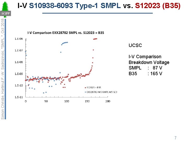
Simon Christie, Hartmut F. -W. Sadrozinski, "SMPL ", Oct 2018 I-V S 10938 -6093 Type-1 SMPL vs. S 12023 (B 35) UCSC I-V Comparison Breakdown Voltage SMPL : 87 V B 35 : 165 V 7
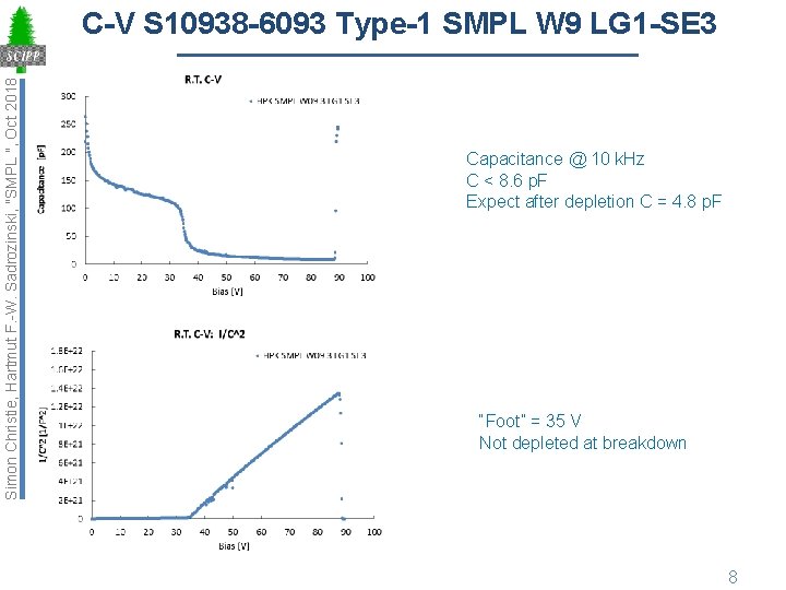
Simon Christie, Hartmut F. -W. Sadrozinski, "SMPL ", Oct 2018 C-V S 10938 -6093 Type-1 SMPL W 9 LG 1 -SE 3 Capacitance @ 10 k. Hz C < 8. 6 p. F Expect after depletion C = 4. 8 p. F “Foot” = 35 V Not depleted at breakdown 8
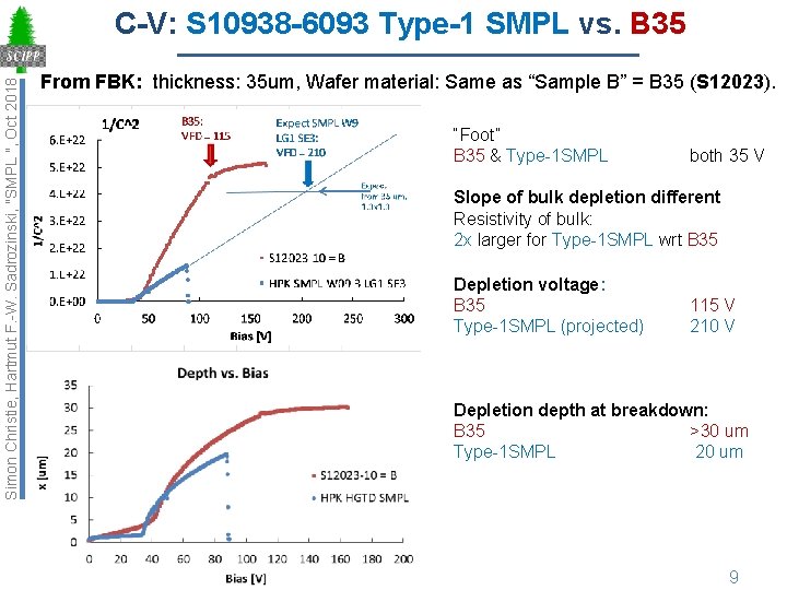
Simon Christie, Hartmut F. -W. Sadrozinski, "SMPL ", Oct 2018 C-V: S 10938 -6093 Type-1 SMPL vs. B 35 From FBK: thickness: 35 um, Wafer material: Same as “Sample B” = B 35 (S 12023). “Foot” B 35 & Type-1 SMPL both 35 V Slope of bulk depletion different Resistivity of bulk: 2 x larger for Type-1 SMPL wrt B 35 Depletion voltage: B 35 Type-1 SMPL (projected) 115 V 210 V Depletion depth at breakdown: B 35 >30 um Type-1 SMPL 20 um 9
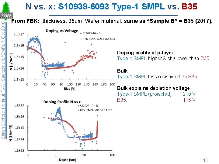
Simon Christie, Hartmut F. -W. Sadrozinski, "SMPL ", Oct 2018 N vs. x: S 10938 -6093 Type-1 SMPL vs. B 35 From FBK: thickness: 35 um, Wafer material: same as “Sample B” = B 35 (2017). Doping profile of p-layer: Type-1 SMPL higher & shallower than B 35 Bulk Type-1 SMPL less resistive than B 35 Bulk explains depletion voltage Type-1 SMPL (projected): 210 V B 35: 115 V 10
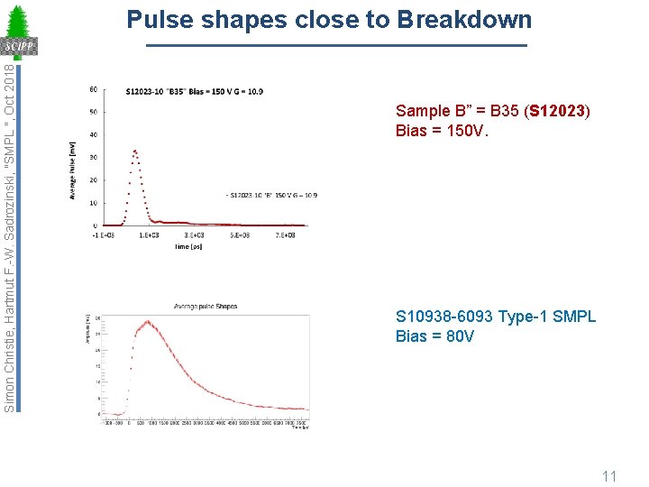
Simon Christie, Hartmut F. -W. Sadrozinski, "SMPL ", Oct 2018 Pulse shapes close to Breakdown Sample B” = B 35 (S 12023) Bias = 150 V. S 10938 -6093 Type-1 SMPL Bias = 80 V 11
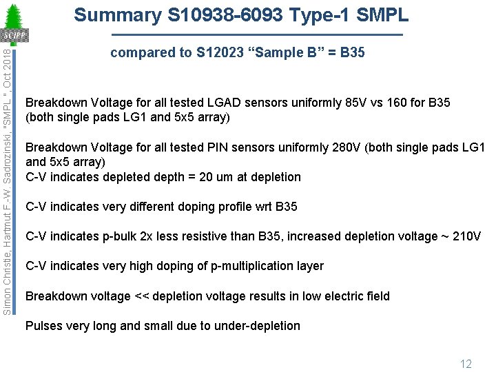
Simon Christie, Hartmut F. -W. Sadrozinski, "SMPL ", Oct 2018 Summary S 10938 -6093 Type-1 SMPL compared to S 12023 “Sample B” = B 35 Breakdown Voltage for all tested LGAD sensors uniformly 85 V vs 160 for B 35 (both single pads LG 1 and 5 x 5 array) Breakdown Voltage for all tested PIN sensors uniformly 280 V (both single pads LG 1 and 5 x 5 array) C-V indicates depleted depth = 20 um at depletion C-V indicates very different doping profile wrt B 35 C-V indicates p-bulk 2 x less resistive than B 35, increased depletion voltage ~ 210 V C-V indicates very high doping of p-multiplication layer Breakdown voltage << depletion voltage results in low electric field Pulses very long and small due to under-depletion 12