Silicon Sensors for Collider Physics from Physics Requirements


- Slides: 34

Silicon Sensors for Collider Physics from Physics Requirements to Vertex Tracking Detectors Marco Battaglia Lawrence Berkeley National Laboratory, University of California at Santa Cruz and CERN, Geneva EDIT 2012, Silicon Track, February 2012

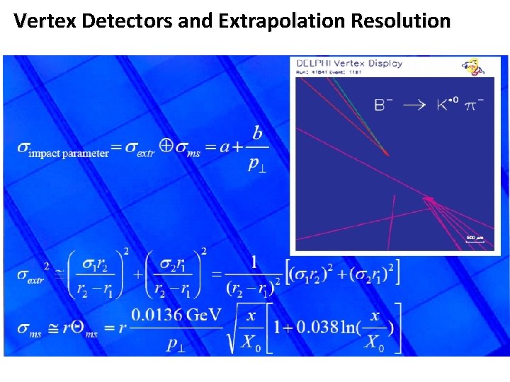
Vertex Detectors and Extrapolation Resolution

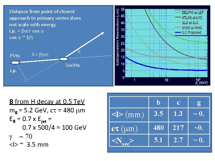
Distance from point of closest approach to primary vertex does not scale with energy i. p. = bgct cos a ~ 1/g PVtx i. p. l = bgct a Sec. Vtx B from H decay at 0. 5 Te. V m. B = 5. 2 Ge. V, ct = 480 mm EB = 0. 7 x Ejet = 0. 7 x 500/4 = 100 Ge. V g ~ 70 <l> ~ 3. 5 mm b c g <l> (mm) 3. 5 1. 3 ~ 0. ct (mm) <Nsec> 480 217 ~0. 5. 1 2. 7 ~ 0.

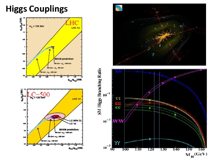
Higgs Couplings

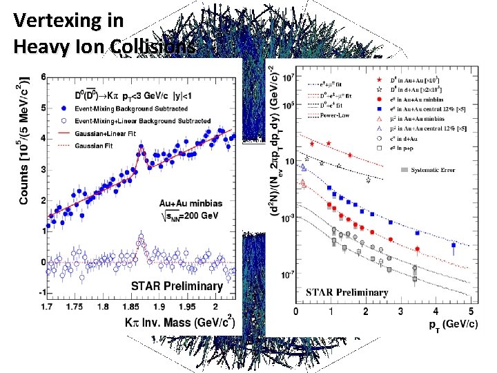
Vertexing in Heavy Ion Collisions (SGV Fast Simulation)

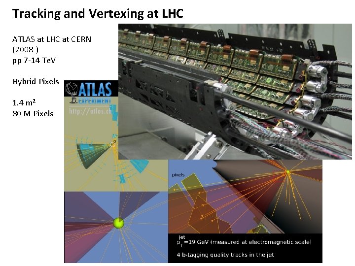
Tracking and Vertexing at LHC ATLAS at LHC at CERN (2008 -) pp 7 -14 Te. V Hybrid Pixels 1. 4 m 2 80 M Pixels

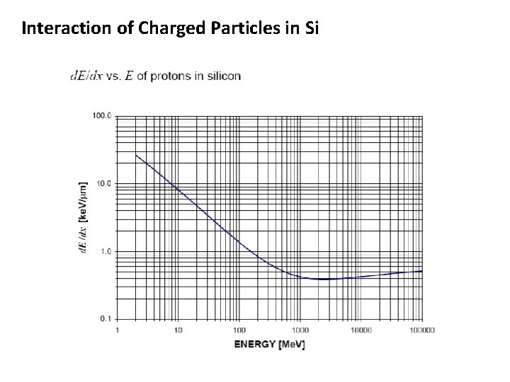
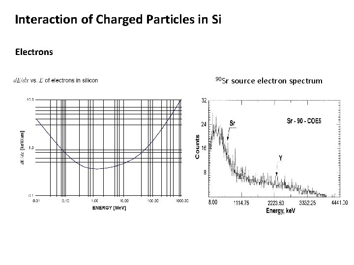
Interaction of Charged Particles in Si

Interaction of Charged Particles in Si

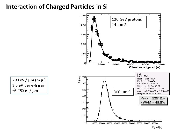
Interaction of Charged Particles in Si 120 Ge. V protons 14 mm Si 280 e. V / mm (m. p. ) 3. 6 e. V per e-h pair ~80 e- / mm 300 mm Si

Interaction of Charged Particles in Si Electrons 90 Sr source electron spectrum

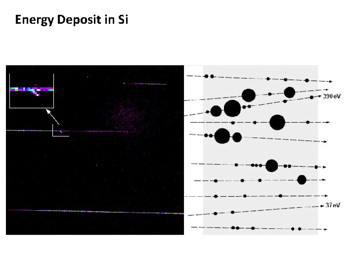
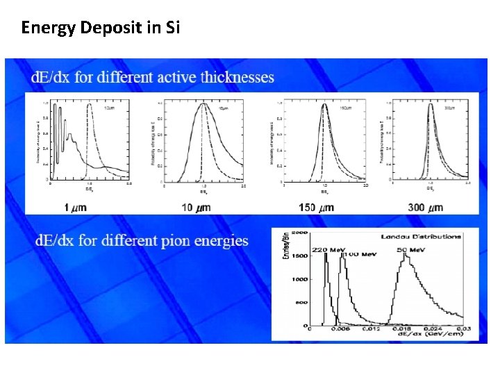
Energy Deposit in Si

Energy Deposit in Si

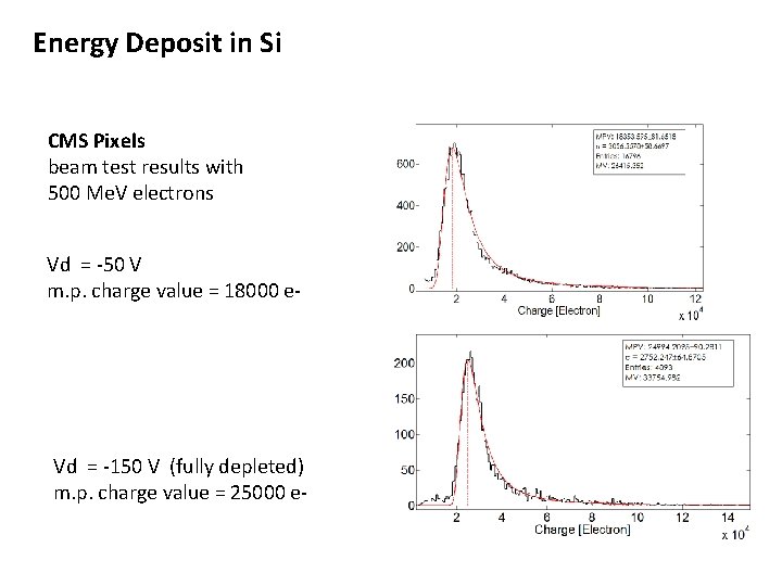
Energy Deposit in Si CMS Pixels beam test results with 500 Me. V electrons Vd = -50 V m. p. charge value = 18000 e- Vd = -150 V (fully depleted) m. p. charge value = 25000 e-

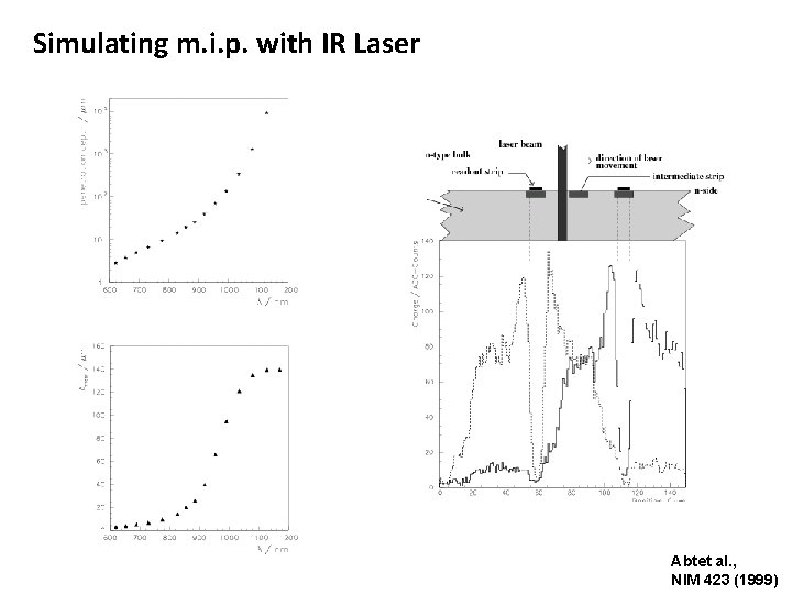
Simulating m. i. p. with IR Laser Abtet al. , NIM 423 (1999)

Position Sensitive Detectors

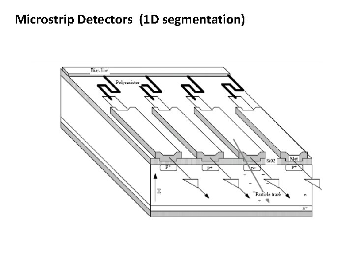
Microstrip Detectors (1 D segmentation)

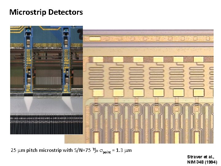
Microstrip Detectors 25 mm pitch microstrip with S/N=75 g spoint = 1. 3 mm Straver et al. , NIM 348 (1994)

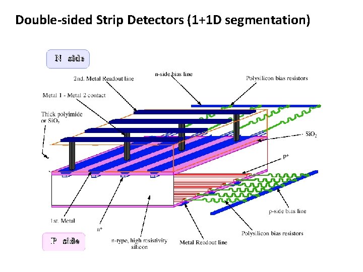
Double-sided Strip Detectors (1+1 D segmentation)

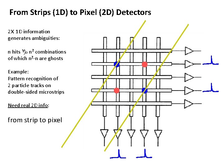
From Strips (1 D) to Pixel (2 D) Detectors 2 x 1 D information generates ambiguities: n hits g n 2 combinations of which n 2 -n are ghosts Example: Pattern recognition of 2 particle tracks on double-sided microstrips Need real 2 D info: from strip to pixel

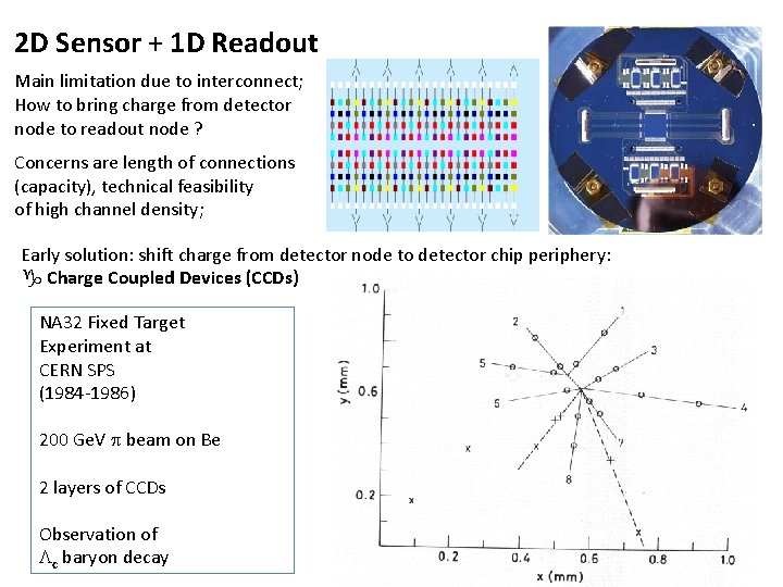
2 D Sensor + 1 D Readout Main limitation due to interconnect; How to bring charge from detector node to readout node ? Concerns are length of connections (capacity), technical feasibility of high channel density; Early solution: shift charge from detector node to detector chip periphery: g Charge Coupled Devices (CCDs) NA 32 Fixed Target Experiment at CERN SPS (1984 -1986) 200 Ge. V p beam on Be 2 layers of CCDs Observation of Lc baryon decay

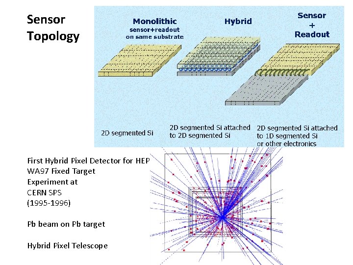
Sensor Topology First Hybrid Pixel Detector for HEP WA 97 Fixed Target Experiment at CERN SPS (1995 -1996) Pb beam on Pb target Hybrid Pixel Telescope

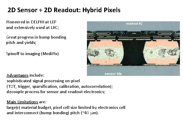
2 D Sensor + 2 D Readout: Hybrid Pixels Pioneered in DELPHI at LEP and extensively used at LHC; Great progress in bump bonding pitch and yields; Spinoff to imaging (Medi. Pix) Advantages include: sophisticated signal processing on-pixel (TOT, trigger, sparsification, calibration, autocorrelation); decouple process for sensor and readout electronics; Main Limitations are: large(r) material budget, pixel cell size limited by electronics cell and interconnect (bump bonding) pitch (~40 mm).

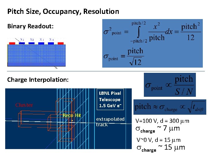
Pitch Size, Occupancy, Resolution Binary Readout: Charge Interpolation: LBNL Pixel Telescope 1. 5 Ge. V e- Cluster Reco Hit extrapolated track V=100 V, d = 300 mm scharge ~ 7 mm V~0 V, d = 15 mm scharge ~ 15 mm

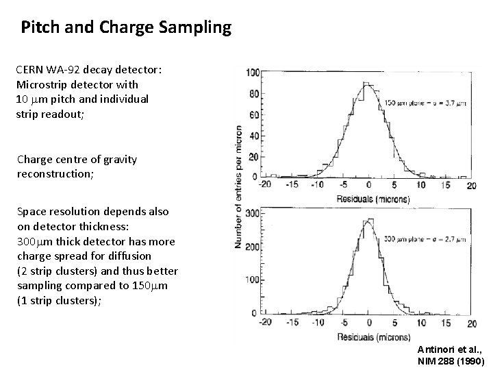
Pitch and Charge Sampling CERN WA-92 decay detector: Microstrip detector with 10 mm pitch and individual strip readout; Charge centre of gravity reconstruction; Space resolution depends also on detector thickness: 300 mm thick detector has more charge spread for diffusion (2 strip clusters) and thus better sampling compared to 150 mm (1 strip clusters); Antinori et al. , NIM 288 (1990)

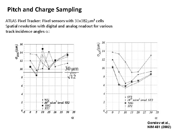
Pitch and Charge Sampling ATLAS Pixel Tracker: Pixel sensors with 30 x 382 mm 2 cells Spatial resolution with digital and analog readout for various track incidence angles a: Gorelov et al. , NIM 481 (2002)

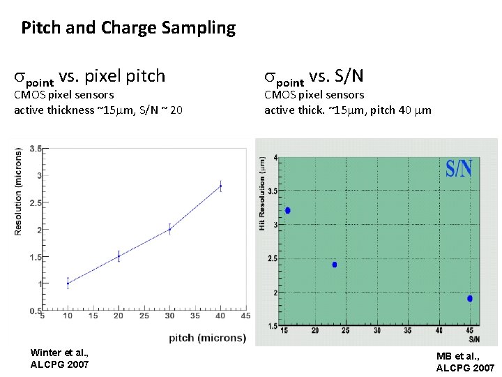
Pitch and Charge Sampling spoint vs. pixel pitch CMOS pixel sensors active thickness ~15 mm, S/N ~ 20 Winter et al. , ALCPG 2007 spoint vs. S/N CMOS pixel sensors active thick. ~15 mm, pitch 40 mm MB et al. , ALCPG 2007

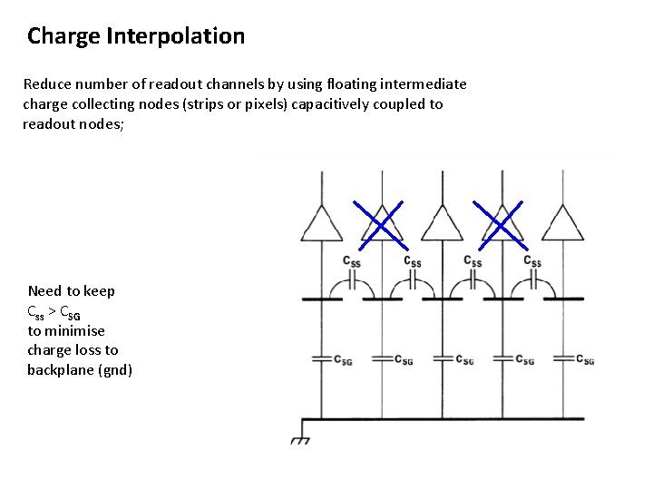
Charge Interpolation Reduce number of readout channels by using floating intermediate charge collecting nodes (strips or pixels) capacitively coupled to readout nodes; Need to keep Css > CSG to minimise charge loss to backplane (gnd)

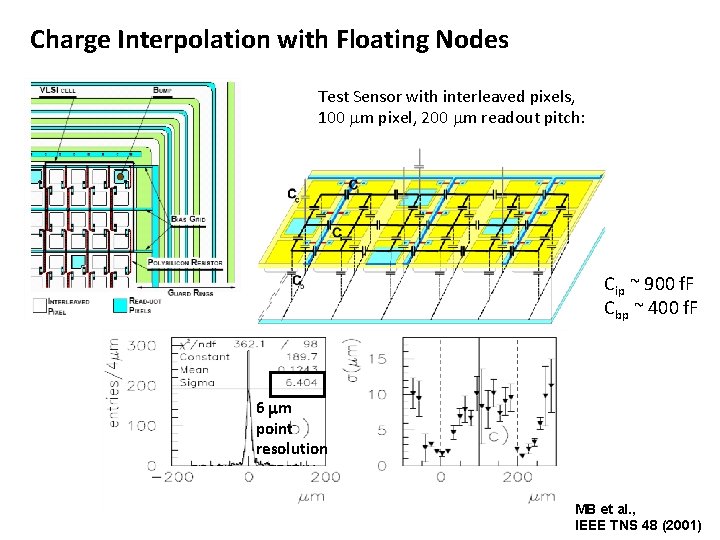
Charge Interpolation with Floating Nodes Test Sensor with interleaved pixels, 100 mm pixel, 200 mm readout pitch: Cip ~ 900 f. F Cbp ~ 400 f. F 6 mm point resolution MB et al. , IEEE TNS 48 (2001)

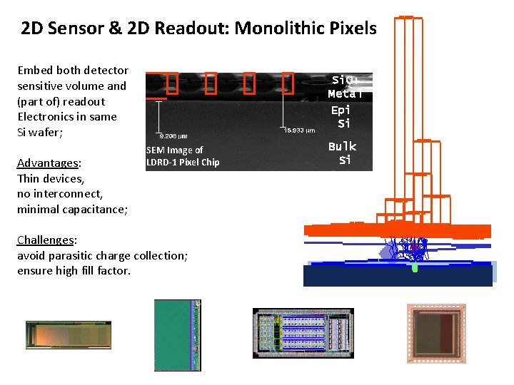
2 D Sensor & 2 D Readout: Monolithic Pixels Embed both detector sensitive volume and (part of) readout Electronics in same Si wafer; Advantages: Thin devices, no interconnect, minimal capacitance; Si. O+ Metal Epi Si SEM Image of LDRD-1 Pixel Chip Challenges: avoid parasitic charge collection; ensure high fill factor. Bulk Si

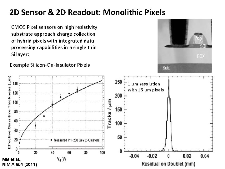
2 D Sensor & 2 D Readout: Monolithic Pixels CMOS Pixel sensors on high resistivity substrate approach charge collection of hybrid pixels with integrated data processing capabilities in a single thin Si layer: Example Silicon-On-Insulator Pixels 1 mm resolution with 15 mm pixels MB et al. , NIM A 654 (2011)

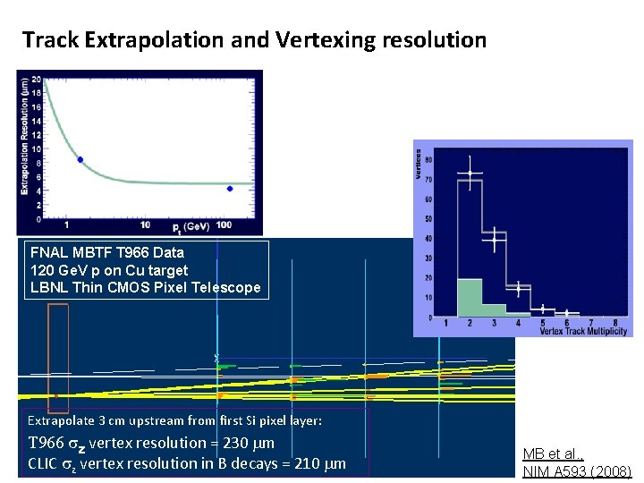
Track Extrapolation and Vertexing resolution FNAL MBTF T 966 Data 120 Ge. V p on Cu target LBNL Thin CMOS Pixel Telescope Extrapolate 3 cm upstream from first Si pixel layer: T 966 sz vertex resolution = 230 mm CLIC sz vertex resolution in B decays = 210 mm MB et al. , NIM A 593 (2008)

Silicon Track Day 2 Microstrip Detectors from D 0 and CDF to be tested with small spot IR laser Microstrip Detector from CMS to be tested with 90 Sr Landau distribution, depletion Hybrid Pixel Detector from CMS to be tested with 90 Sr DAQ and readout chip, chip calibration, threshold scan, Landau distribution, scaling of collected charge vs Vd, cluster analysis CMOS Monolithic Pixel Detector to be tested with 90 Sr (and IR laser) Visualization of analog pixel signal on oscilloscope, driving clocks, Landau distribution, determination of sensitive thickness, d ray visalization, cluster reconstruction and analysis

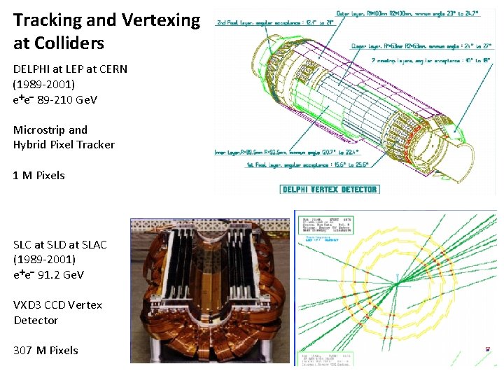
Tracking and Vertexing at Colliders DELPHI at LEP at CERN (1989 -2001) e+e- 89 -210 Ge. V Microstrip and Hybrid Pixel Tracker 1 M Pixels SLC at SLD at SLAC (1989 -2001) e+e- 91. 2 Ge. V VXD 3 CCD Vertex Detector 307 M Pixels

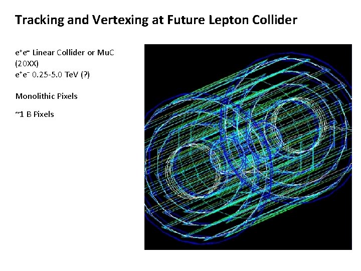
Tracking and Vertexing at Future Lepton Collider e+e- Linear Collider or Mu. C (20 XX) e+e- 0. 25 -5. 0 Te. V (? ) Monolithic Pixels ~1 B Pixels