SILICON MICROMACHINING Definition Si micromachining refers to fashioning


-plane is")


 : Mechanical Velcro (I) Objective : To apply isotropic and anisotropic wet")
 Process Flow The caps are 1. 0 mm of Si. O 2 atop")
 Mechanical Testing : Method • Patterned samples, nominally 8 mm x 8 mm")
 Mechanical Testing : Results")
 Analysis Assuming simple cantilever : • The bending stress, s, is y is")
 : The")
 : Undoped Cantilever Si Beams (I) Objective : To fabricate cantilever beams")
 Flow Process : Masks To construct a Si cantilever beam of width Wb,")
 Process Flow : Etching")
")
 : Straight Cantilever Beam with Integrated Al Electrodes (I) Objective : To")
 Process Flow")

 Process Flow (ctd) :")

- Slides: 21
SILICON MICROMACHINING Definition Si micromachining refers to fashioning microscopic mechanical parts out of a silicon substrate or on a silicon substrate. Bulk Micromachining (emerged in early 1960's) • Is utilized in the manufacturing of the majority of commercial devices ; almost all of pressure sensors and Si valves. • It is used to realize structures within the bulk of a single crystal Si wafer by selectively removing wafer material. • Structures may cover the thickness range from submicron to full wafer thickness (~500 mm), and lateral dimensions as large as few millimeters. Surface Micromachining (emerged in early 1980's) • Structures are mainly located on the surface of the Si wafer and consist of thin films. • The dimensions of structures can be several orders of magnitude smaller than structures generated by bulk micromachining
SILICON BULK MICROMACHINING • Lithography and etching are the key technological steps for bulk micromachining. • Basic Etch Steps : – (i) Wet isotropic etching. – (ii) Wet anisotropic etching. – (iii) Plasma isotropic etching. – (iv) Reactive ion etching (RIE). – (v) Etchstop techniques.
Isotropic and Anisotropic Wet Etching • In diamond and zinc-blend lattices, the (111)-plane is more closely packed than the (100)-plane and, hence, for any given etchant the etch rate is expected to be slower for the (111) plane. • For most wet etchants this difference in etch rates with orientation is insignificant : the result is that with most wet etchants etching is isotropic. • However, some wet etchants have the property of dissolving a given crystal plane of a semiconductor much faster than other planes ; i. e. , these etchants have etch rates that are orientation dependent.
Anisotropic Etching Characteristics of Crystalline Si • The width of the bottom surface, W, is Wo is the width of the window on the wafer surface an h is the etched depth.
Anisotropic Etching Characteristics of Crystalline Si
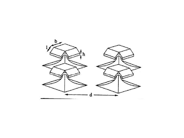
Example (1) : Mechanical Velcro (I) Objective : To apply isotropic and anisotropic wet etching to fabricate dense regular arrays of microstructures which act as surface adhesives. Han etal. , JMEMS 1(1), 37 (1992)
(II) Process Flow The caps are 1. 0 mm of Si. O 2 atop Si pedestals.
(III) Mechanical Testing : Method • Patterned samples, nominally 8 mm x 8 mm were interlocked by applying a load to the upper substrate ; the insertion pressure was monitored by placing the entire assembly on an electronic force scale. • The bond strength of the mating structures was characterized by direct measurements of the tensile load needed to induce failure : bond strength is determined by applying a tensile load through a pulley and measuring the force necessary for separation. • Separation of the samples (failure) is always accompanied by damaged areas on corresponding regions of the mating surfaces : this is interpreted as the samples interlocking only over damaged regions. • The fraction of damaged area was found to be proportional to the initial loading (insertion pressure).
(III) Mechanical Testing : Results
(IV) Analysis Assuming simple cantilever : • The bending stress, s, is y is the distance from the neutral surface. b and h are the width and thickness of the rectangular crosssection. • For x = 0 and y = ± h/2 Pn is the interaction force between the tabs and l is the length of the tab.
The maximum shearing stress is at the neutral surface (y = 0) : The ratio of the two stresses is Measurements indicate that failure occurs when From the figure : Using : We get : Substituting design values :
Example (2) : Undoped Cantilever Si Beams (I) Objective : To fabricate cantilever beams oriented in the (100) direction on (100) silicon wafers. Choi and Smits ; JMEMS, 2(2), 82 (1993)
(II) Flow Process : Masks To construct a Si cantilever beam of width Wb, thickness tb, and length lb. For mask 1 (etching in Na. OH) : To free the Si cantilever in the second Na. OH etching, we need for mask 2 : W 1 = 190 mm, W 2 = 110 mm, d = 300 mm, and l 1 =l 2 = {450, 680, 900, 1360, 1810} mm.
(III) Process Flow : Etching
Dry-Etching Based Bulk Micromachining • The type, shape and size of single-crystal silicon (SCS) structures that can be fabricated using anisotropic wet chemical etch techniques are severely limited. • Dry-etch based processes have been developed. • The most important of these processes is a process called SCREAM for single crystal reactive etching and metallization process. • SCREAM uses RIE processes to fabricate released SCS structures with lateral feature sizes down to 250 nm and with arbitrary structure orientations on a Si wafer. • SCREAM includes process options to make integrated, side-drive capacitor actuators. • A compatible high step-coverage metallization process using metal sputter deposition and isotropic metal dry etch is used to form side-drive electrodes. This metallization process complements the Si RIE processes used to form the movable SCS structures.
Example (3) : Straight Cantilever Beam with Integrated Al Electrodes (I) Objective : To fabricate a free-standing cantilever beam 200 mm long, 0. 8 mm wide, and 3. 5 mm thick coated with a 150 nm thick silicon dioxide layer. Zhang and Mac. Donald, JMM, pp. 31 -38 (1992).
(II) Process Flow
Silicon Etch Parameters
(II) Process Flow (ctd) :
SEM Micrographs of Silicon Etch Profiles