Silicon detectors Lecture 10 Readout data acquisition board
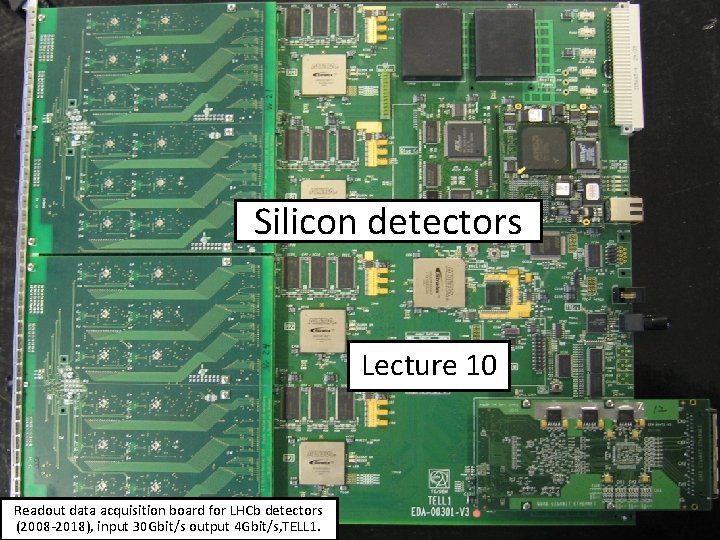
Silicon detectors Lecture 10 Readout data acquisition board for LHCb detectors (2008 -2018), input 30 Gbit/s output 4 Gbit/s, TELL 1.
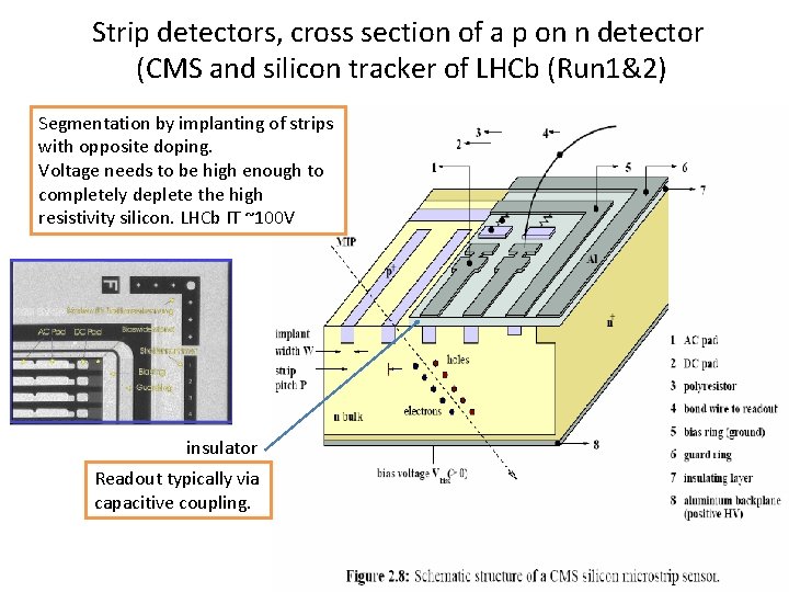
Strip detectors, cross section of a p on n detector (CMS and silicon tracker of LHCb (Run 1&2) Segmentation by implanting of strips with opposite doping. Voltage needs to be high enough to completely deplete the high resistivity silicon. LHCb IT ~100 V insulator Readout typically via capacitive coupling.
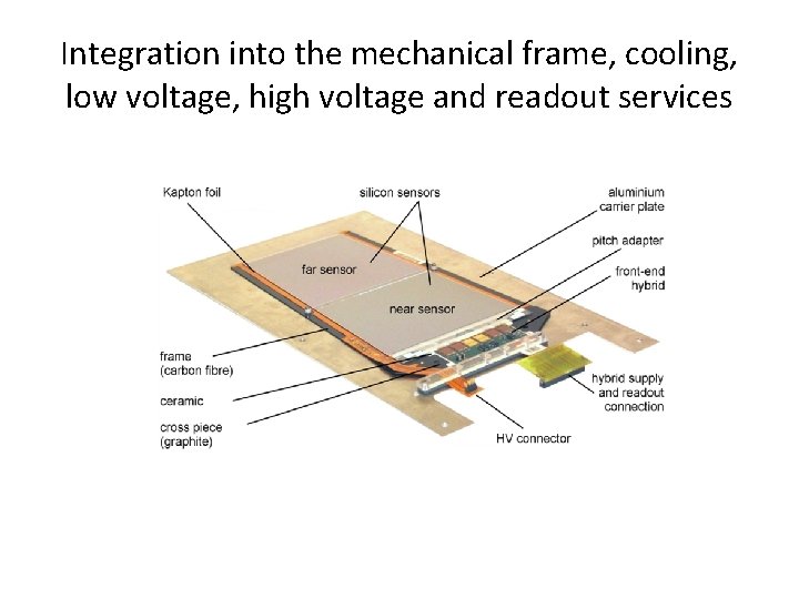
Integration into the mechanical frame, cooling, low voltage, high voltage and readout services

Large Si strip detectors
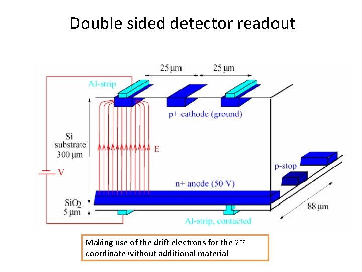
Double sided detector readout Making use of the drift electrons for the 2 nd coordinate without additional material
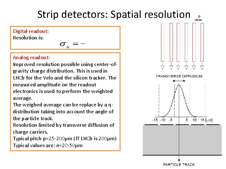
Strip detectors: Spatial resolution Digital readout: Resolution is: Analog readout: Improved resolution possible using center-ofgravity charge distribution. This is used in LHCb for the Velo and the silicon tracker. The measured amplitude on the readout electronics is used to perform the weighted average. The weighed average can be replace by a ηdistribution taking into account the angle of the particle track. Resolution limited by transverse diffusion of charge carriers. Typical pitch p=25 -200µm (IT LHCb is 200µm) Typical values are: σ=20 -50µm
![Some history of silicon detectors Experiment # Sensors # Channels Area [m 2] CMS Some history of silicon detectors Experiment # Sensors # Channels Area [m 2] CMS](http://slidetodoc.com/presentation_image_h2/3ed4f604dbb695b54082f96d91241a82/image-7.jpg)
Some history of silicon detectors Experiment # Sensors # Channels Area [m 2] CMS 15. 95 K 10 M 223 Atlas 16 K 6. 1 M 60 AMS 2 2. 3 K 196 K 6. 5 CDF SVXII 720 405 1. 9 140 K 0. 95 Babar Aleph 144 95 K 0. 49 L 3 96 86 K 0. 23
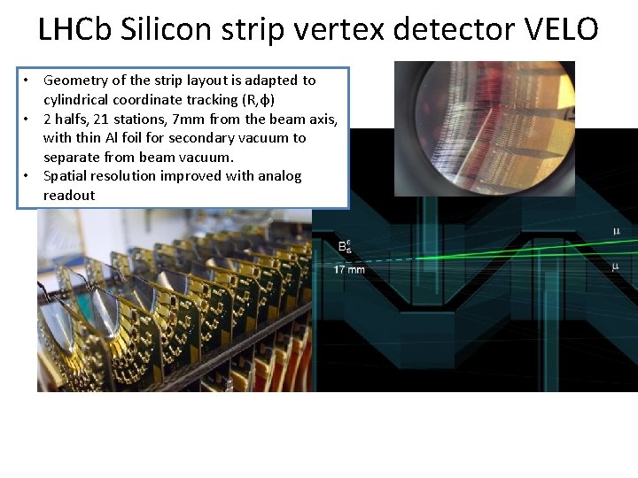
LHCb Silicon strip vertex detector VELO • Geometry of the strip layout is adapted to cylindrical coordinate tracking (R, φ) • 2 halfs, 21 stations, 7 mm from the beam axis, with thin Al foil for secondary vacuum to separate from beam vacuum. • Spatial resolution improved with analog readout
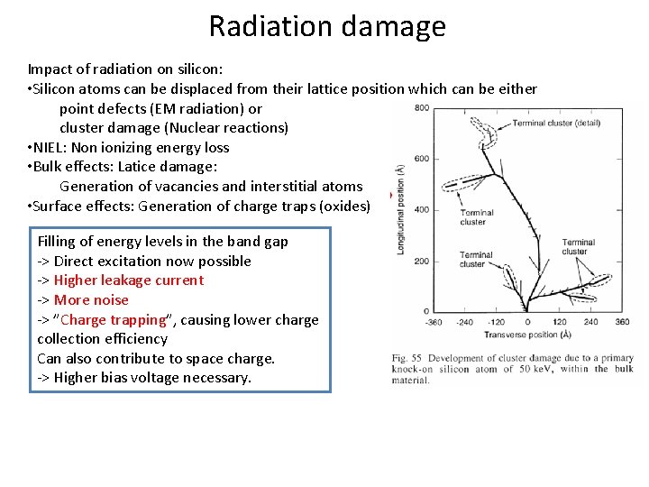
Radiation damage Impact of radiation on silicon: • Silicon atoms can be displaced from their lattice position which can be either point defects (EM radiation) or cluster damage (Nuclear reactions) • NIEL: Non ionizing energy loss • Bulk effects: Latice damage: Generation of vacancies and interstitial atoms • Surface effects: Generation of charge traps (oxides) Filling of energy levels in the band gap -> Direct excitation now possible -> Higher leakage current -> More noise -> ”Charge trapping”, causing lower charge collection efficiency Can also contribute to space charge. -> Higher bias voltage necessary.
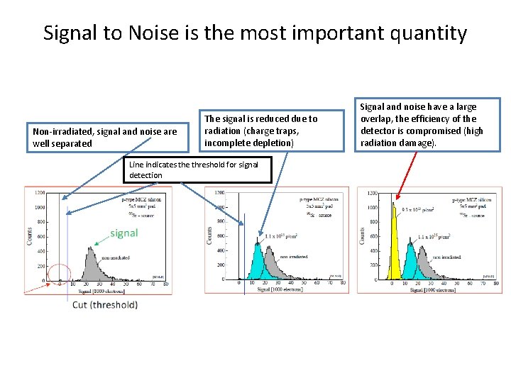
Signal to Noise is the most important quantity Non-irradiated, signal and noise are well separated The signal is reduced due to radiation (charge traps, incomplete depletion) Line indicates the threshold for signal detection Signal and noise have a large overlap, the efficiency of the detector is compromised (high radiation damage).
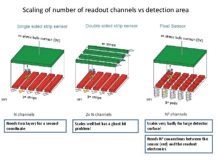
Scaling of number of readout channels vs detection area Needs two layers for a second coordinate Scales well but has a ghost hit problem! Scales very badly for large detector surface! Needs N 2 connections between the sensor (red) and the readout electronics.
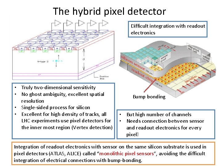
The hybrid pixel detector Difficult integration with readout electronics • Truly two-dimensional sensitivity • No ghost ambiguity, excellent spatial resolution • Single-sided process for silicon • Excellent for high density of tracks, all LHC experiments use pixel detectors for the inner most region (Vertex detection) Bump bonding • But high number of channels • Needs connection between sensor and readout electronics for every pixel! Integration of readout electronics with sensor on the same silicon substrate is used in pixel detectors (ATLAS, ALICE) called “monolithic pixel sensors”, avoiding the difficult integration of electrical connections with bump-bonding.
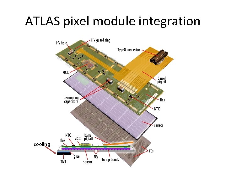
ATLAS pixel module integration cooling
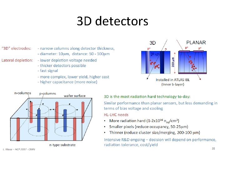
3 D detectors
- Slides: 14