Silicon Bipolar Technologies In BJT the currentflow across
Silicon Bipolar Technologies • In BJT, the current-flow across one of the pn junctions (BC) is modulated by the bias of the other junction (EB). • In forward active region, EB junction is forward biased, and BC junction is reverse biased. • Important parameters are: – = IC /IE = ~1; and = IC/IB = large – In a good transistor, emitter doping is high (>1 E 20 cm-3), base doping is ~1 E 17 cm-3, and collector doping is ~1 E 16 cm-3. – Base width should be low compared to the minority carrier diffusion length in base. • Need isolation between transistors in ICs
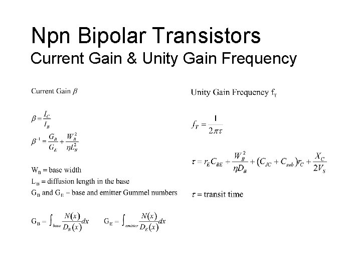
Npn Bipolar Transistors Current Gain & Unity Gain Frequency
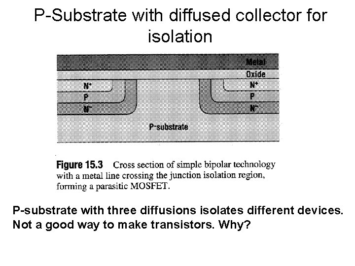
P-Substrate with diffused collector for isolation P-substrate with three diffusions isolates different devices. Not a good way to make transistors. Why?
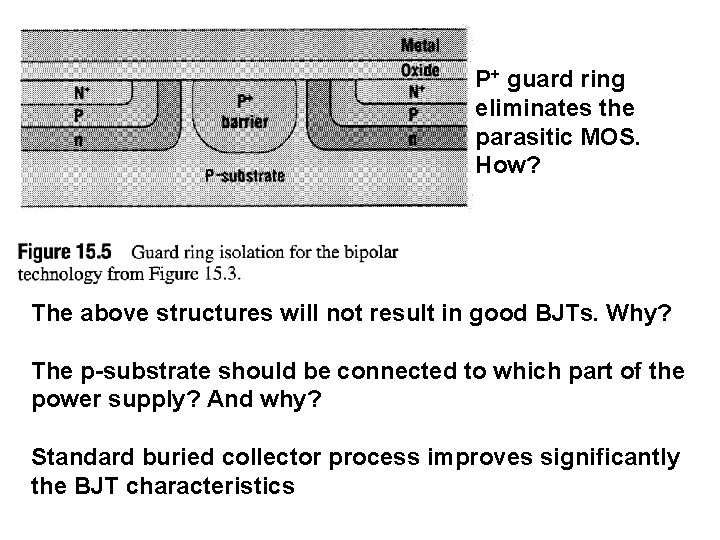
P+ guard ring eliminates the parasitic MOS. How? The above structures will not result in good BJTs. Why? The p-substrate should be connected to which part of the power supply? And why? Standard buried collector process improves significantly the BJT characteristics

Npn Bipolar Transistors Standard Buried Collector (SBC) Process Collector Base Isolation Emitter Isolation
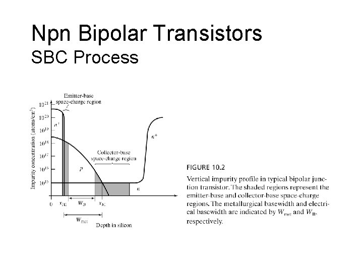
Npn Bipolar Transistors SBC Process
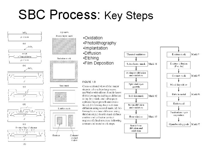
SBC Process: Key Steps • Oxidation • Photolithography • Implantation • Diffusion • Etching • Film Deposition
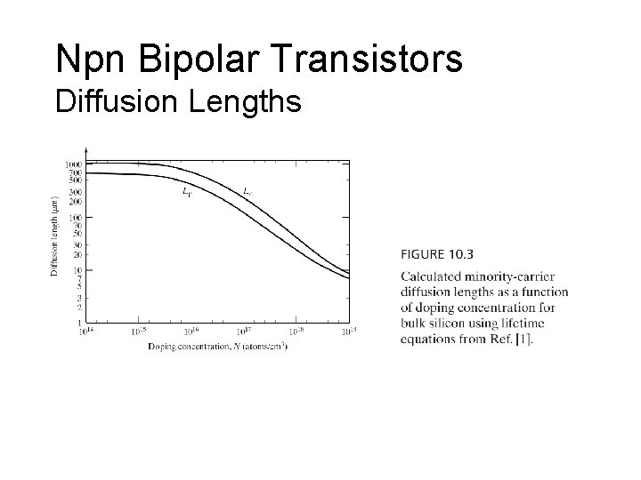
Npn Bipolar Transistors Diffusion Lengths
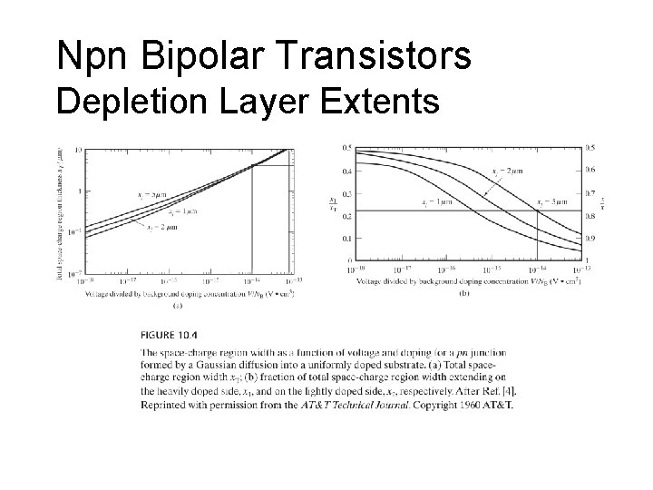
Npn Bipolar Transistors Depletion Layer Extents
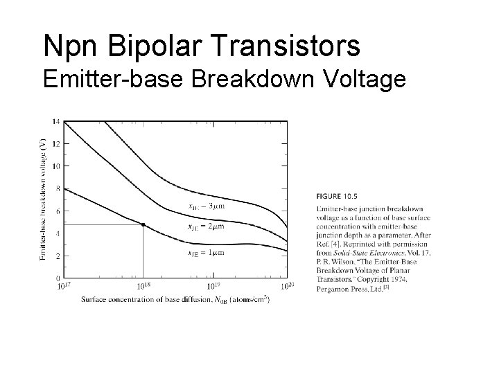
Npn Bipolar Transistors Emitter-base Breakdown Voltage
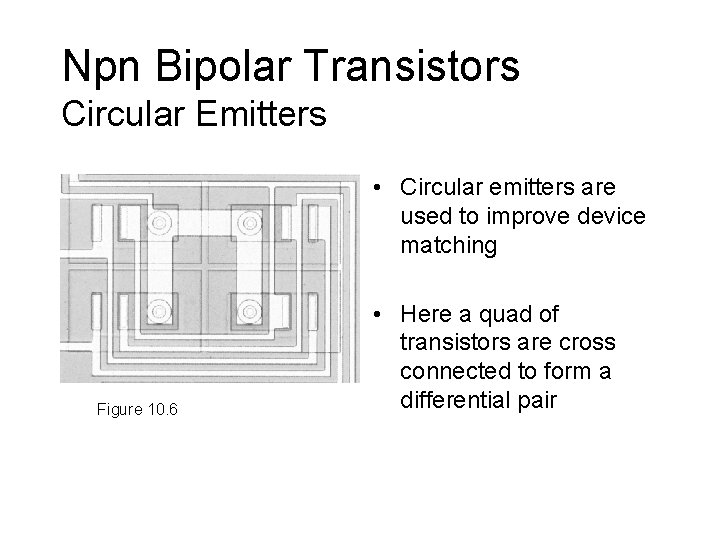
Npn Bipolar Transistors Circular Emitters • Circular emitters are used to improve device matching Figure 10. 6 • Here a quad of transistors are cross connected to form a differential pair

Npn Bipolar Transistors Punch-through Voltage
Questions on SBC process for BJT - Why do we need the buried layer? - What is the approximate doping for the P-substrate? - What part of the power supply the p+-isolation region should be connected? - Why do we need n+-diffusion under the collector contact? - What determines the buried layer dopant? - How many masks will be required to complete the device?
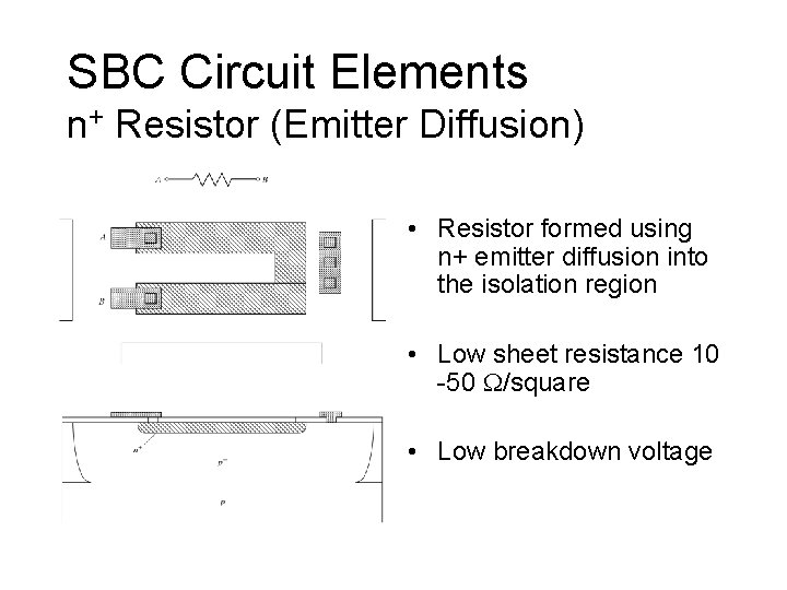
SBC Circuit Elements n+ Resistor (Emitter Diffusion) • Resistor formed using n+ emitter diffusion into the isolation region • Low sheet resistance 10 -50 W/square • Low breakdown voltage
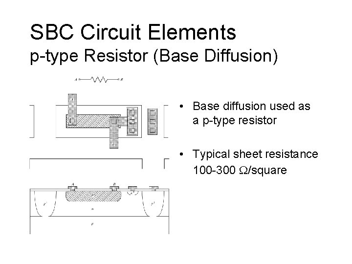
SBC Circuit Elements p-type Resistor (Base Diffusion) • Base diffusion used as a p-type resistor • Typical sheet resistance 100 -300 W/square
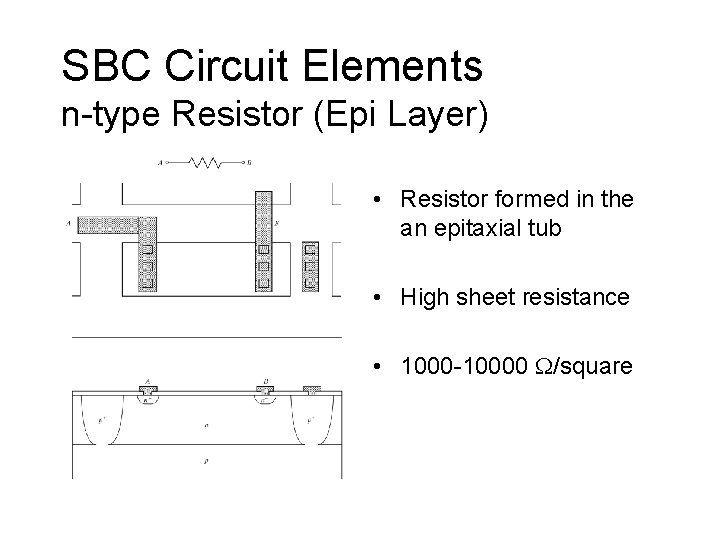
SBC Circuit Elements n-type Resistor (Epi Layer) • Resistor formed in the an epitaxial tub • High sheet resistance • 1000 -10000 W/square
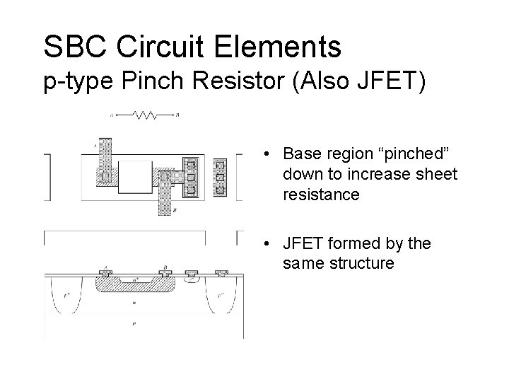
SBC Circuit Elements p-type Pinch Resistor (Also JFET) • Base region “pinched” down to increase sheet resistance • JFET formed by the same structure
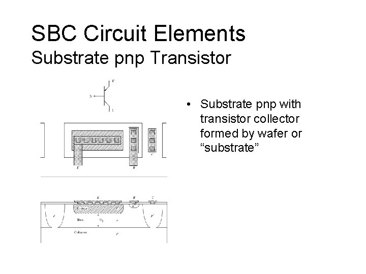
SBC Circuit Elements Substrate pnp Transistor • Substrate pnp with transistor collector formed by wafer or “substrate”
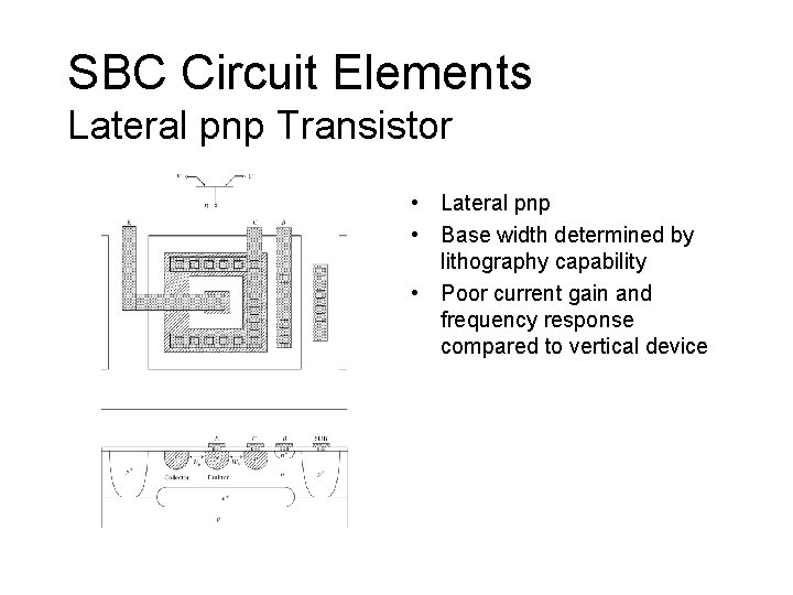
SBC Circuit Elements Lateral pnp Transistor • Lateral pnp • Base width determined by lithography capability • Poor current gain and frequency response compared to vertical device
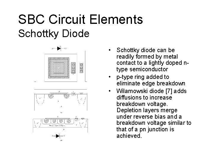
SBC Circuit Elements Schottky Diode • Schottky diode can be readily formed by metal contact to a lightly doped ntype semiconductor • p-type ring added to eliminate edge breakdown • Wilamowski diode [7] adds diffusions to increase breakdown voltage. Depletion layers merge under reverse bias and a breakdown voltage similar to that of a pn junction is achieved.
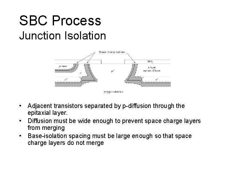
SBC Process Junction Isolation • Adjacent transistors separated by p-diffusion through the epitaxial layer. • Diffusion must be wide enough to prevent space charge layers from merging • Base-isolation spacing must be large enough so that space charge layers do not merge
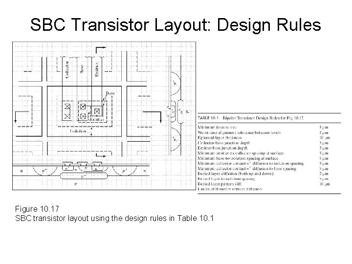
SBC Transistor Layout: Design Rules Figure 10. 17 SBC transistor layout using the design rules in Table 10. 1
Improvements on the standard SBC BJT process • In all modern BJT process, the p+-isolation diffusion is replaced by the LOCOS. This results in much better device since reverse leakage is reduced significantly. Also junction curvature is eliminated, thus increasing the BC breakdown voltage. • Si 3 N 4 mask is used as the local oxidation mask. • Doped polysilicon is extensively used as the diffusion source for emitter to reduce the ion implantation damage.
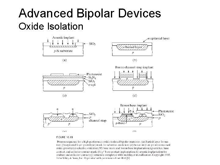
Advanced Bipolar Devices Oxide Isolation
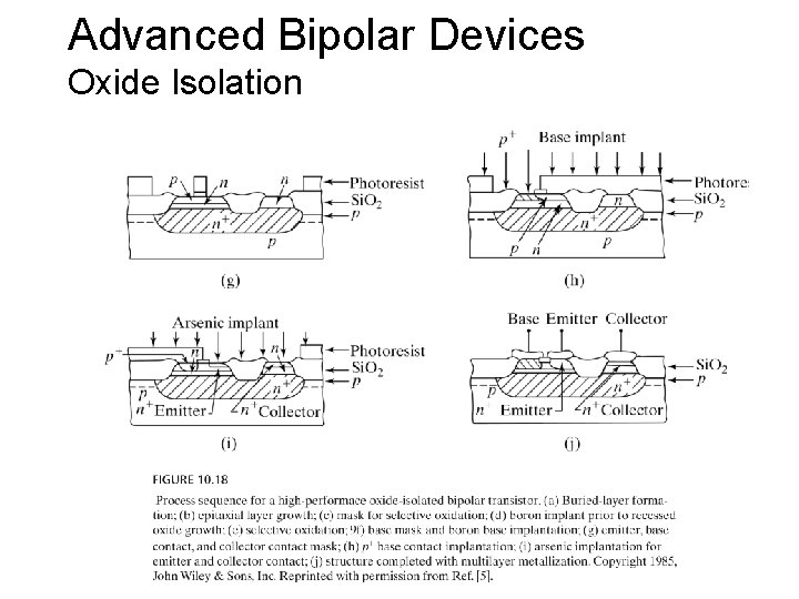
Advanced Bipolar Devices Oxide Isolation
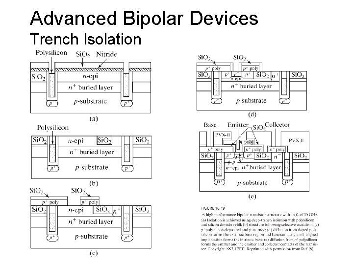
Advanced Bipolar Devices Trench Isolation

Advanced Bipolar Devices Si. Ge HBT
Related Issues • Sb for buried layers: – Good dopant - if auto-doping is a concern (true in batch process, but less so in single wafer low pressure CVD). Also, it diffuses less. – Problems: It is a big atom, so solid solubility is low. So, sheet resistance after doping is about 70 ohm/square compared to 25 ohm/square for As. Another problem is the difficulty in growing good epi after Sb doping. This is because Sb is a bigger atom, and causes lattice distortion. • So, As is used as the buried layer doping now.
Other advantages of Poly-Si emitter technology • Self aligned emitter contact to emitter doping. Increased packing in VLSI, and hence faster device • Poly-Si as the doping source results in highly doped shallow emitter since final doping is done at the last stage of anneal. • The external metal contact is physically isolated from the intrinsic emitter. This prevents metal contact shorting of emitter(? ). • The poly-silicon is used as the local interconnect without any extra processing.
- Slides: 29