Signal Formation in Particle Detectors Werner Riegler CERN
- Slides: 59

Signal Formation in Particle Detectors Werner Riegler, CERN, werner. riegler@cern. ch II Seminario Nazionale Rivelatori Innovativi 18 -22 October 2010, Trieste Lecture 3/3 Signals in Detectors W. Riegler/CERN 1

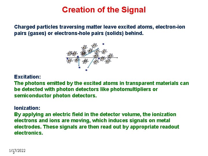
Creation of the Signal Charged particles traversing matter leave excited atoms, electron-ion pairs (gases) or electrons-hole pairs (solids) behind. Excitation: The photons emitted by the excited atoms in transparent materials can be detected with photon detectors like photomultipliers or semiconductor photon detectors. Ionization: By applying an electric field in the detector volume, the ionization electrons and ions are moving, which induces signals on metal electrodes. These signals are then read out by appropriate readout electronics. 1/17/2022 2

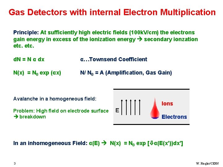
Gas Detectors with internal Electron Multiplication Principle: At sufficiently high electric fields (100 k. V/cm) the electrons gain energy in excess of the ionization energy secondary ionzation etc. d. N = N α dx α…Townsend Coefficient N(x) = N 0 exp (αx) N/ N 0 = A (Amplification, Gas Gain) Avalanche in a homogeneous field: Problem: High field on electrode surface breakdown Ions E Electrons In an inhomogeneous Field: α(E) N(x) = N 0 exp [ α(E(x’))dx’] 3 W. Riegler/CERN

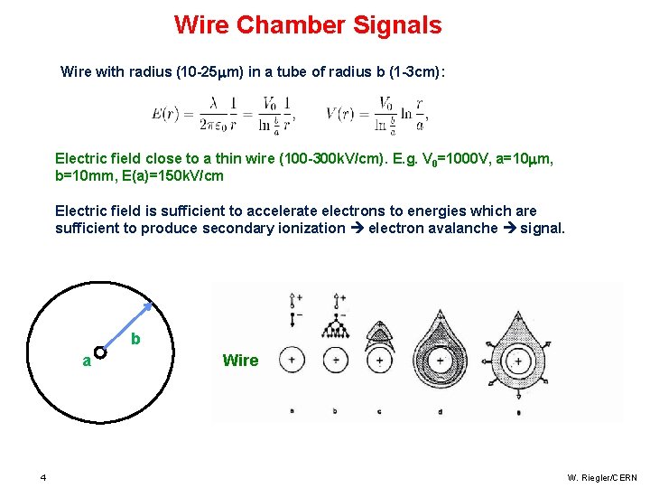
Wire Chamber Signals Wire with radius (10 -25 m) in a tube of radius b (1 -3 cm): Electric field close to a thin wire (100 -300 k. V/cm). E. g. V 0=1000 V, a=10 m, b=10 mm, E(a)=150 k. V/cm Electric field is sufficient to accelerate electrons to energies which are sufficient to produce secondary ionization electron avalanche signal. ab 4 b Wire W. Riegler/CERN

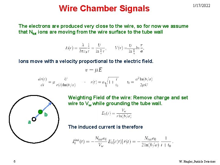
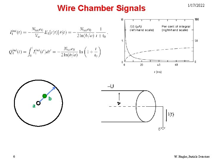
1/17/2022 Wire Chamber Signals The electrons are produced very close to the wire, so for now we assume that Ntot ions are moving from the wire surface to the tube wall Ions move with a velocity proportional to the electric field. Weighting Field of the wire: Remove charge and set wire to Vw while grounding the tube wall. ab 5 b The induced current is therefore W. Riegler, Particle Detectors

Wire Chamber Signals ab 6 1/17/2022 b W. Riegler, Particle Detectors

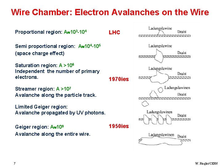
Wire Chamber: Electron Avalanches on the Wire Proportional region: A 103 -104 LHC Semi proportional region: A 104 -105 (space charge effect) Saturation region: A >106 Independent the number of primary electrons. 1970 ies Streamer region: A >107 Avalanche along the particle track. Limited Geiger region: Avalanche propagated by UV photons. Geiger region: A 109 Avalanche along the entire wire. 7 1950 ies W. Riegler/CERN

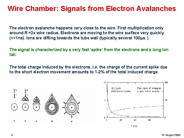
Wire Chamber: Signals from Electron Avalanches The electron avalanche happens very close to the wire. First multiplication only around R =2 x wire radius. Electrons are moving to the wire surface very quickly (<<1 ns). Ions are difting towards the tube wall (typically several 100 s. ) The signal is characterized by a very fast ‘spike’ from the electrons and a long Ion tail. The total charge induced by the electrons, i. e. the charge of the current spike due to the short electron movement amounts to 1 -2% of the total induced charge. 8 W. Riegler/CERN

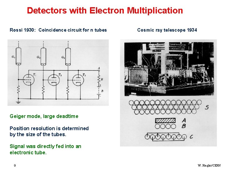
Detectors with Electron Multiplication Rossi 1930: Coincidence circuit for n tubes Cosmic ray telescope 1934 Geiger mode, large deadtime Position resolution is determined by the size of the tubes. Signal was directly fed into an electronic tube. 9 W. Riegler/CERN

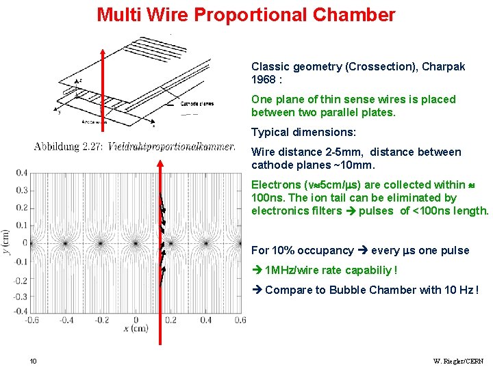
Multi Wire Proportional Chamber Classic geometry (Crossection), Charpak 1968 : One plane of thin sense wires is placed between two parallel plates. Typical dimensions: Wire distance 2 -5 mm, distance between cathode planes ~10 mm. Electrons (v 5 cm/ s) are collected within 100 ns. The ion tail can be eliminated by electronics filters pulses of <100 ns length. For 10% occupancy every s one pulse 1 MHz/wire rate capabiliy ! Compare to Bubble Chamber with 10 Hz ! 10 W. Riegler/CERN

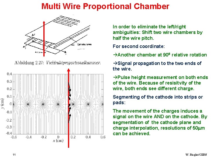
Multi Wire Proportional Chamber In order to eliminate the left/right ambiguities: Shift two wire chambers by half the wire pitch. For second coordinate: àAnother chamber at 900 relative rotation àSignal propagation to the two ends of the wire. àPulse height measurement on both ends of the wire. Because of resisitvity of the wire, both ends see different charge. Segmenting of the cathode into strips or pads: The movement of the charges induces a signal on the wire AND on the cathode. By segmentation of the cathode plane and charge interpolation, resolutions of 50 m can be achieved. 11 W. Riegler/CERN

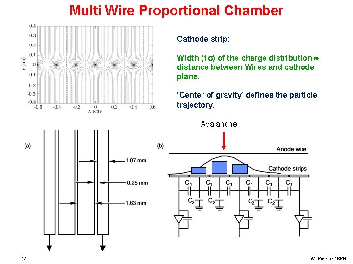
Multi Wire Proportional Chamber Cathode strip: Width (1 ) of the charge distribution distance between Wires and cathode plane. ‘Center of gravity’ defines the particle trajectory. Avalanche 12 W. Riegler/CERN

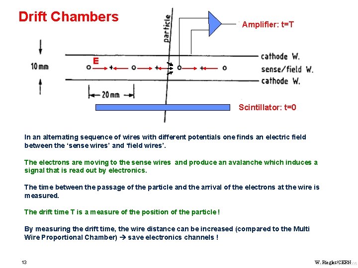
Drift Chambers Amplifier: t=T E Scintillator: t=0 In an alternating sequence of wires with different potentials one finds an electric field between the ‘sense wires’ and ‘field wires’. The electrons are moving to the sense wires and produce an avalanche which induces a signal that is read out by electronics. The time between the passage of the particle and the arrival of the electrons at the wire is measured. The drift time T is a measure of the position of the particle ! By measuring the drift time, the wire distance can be increased (compared to the Multi Wire Proportional Chamber) save electronics channels ! 13 W. Riegler/CERN

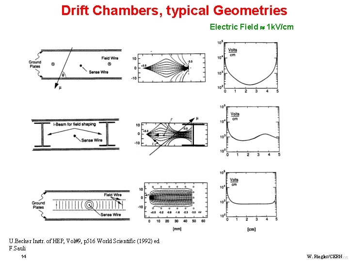
Drift Chambers, typical Geometries Electric Field 1 k. V/cm U. Becker Instr. of HEP, Vol#9, p 516 World Scientific (1992) ed F. Sauli 14 W. Riegler/CERN

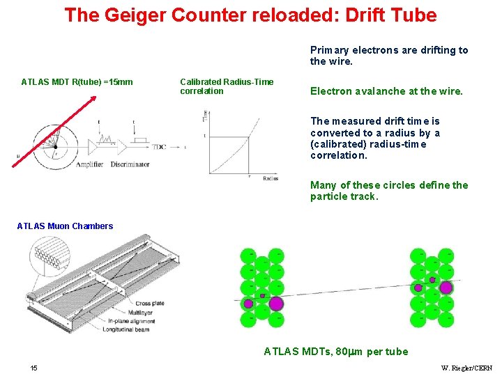
The Geiger Counter reloaded: Drift Tube Primary electrons are drifting to the wire. ATLAS MDT R(tube) =15 mm Calibrated Radius-Time correlation Electron avalanche at the wire. The measured drift time is converted to a radius by a (calibrated) radius-time correlation. Many of these circles define the particle track. ATLAS Muon Chambers ATLAS MDTs, 80 m per tube 15 W. Riegler/CERN

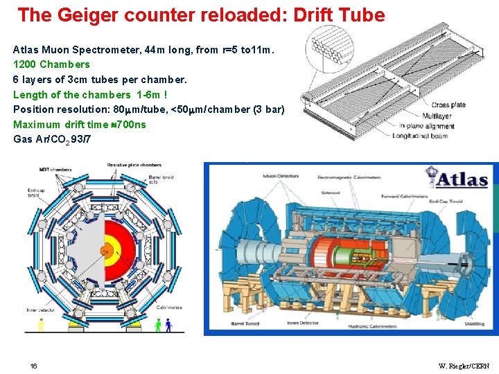
The Geiger counter reloaded: Drift Tube Atlas Muon Spectrometer, 44 m long, from r=5 to 11 m. 1200 Chambers 6 layers of 3 cm tubes per chamber. Length of the chambers 1 -6 m ! Position resolution: 80 m/tube, <50 m/chamber (3 bar) Maximum drift time 700 ns Gas Ar/CO 2 93/7 16 W. Riegler/CERN

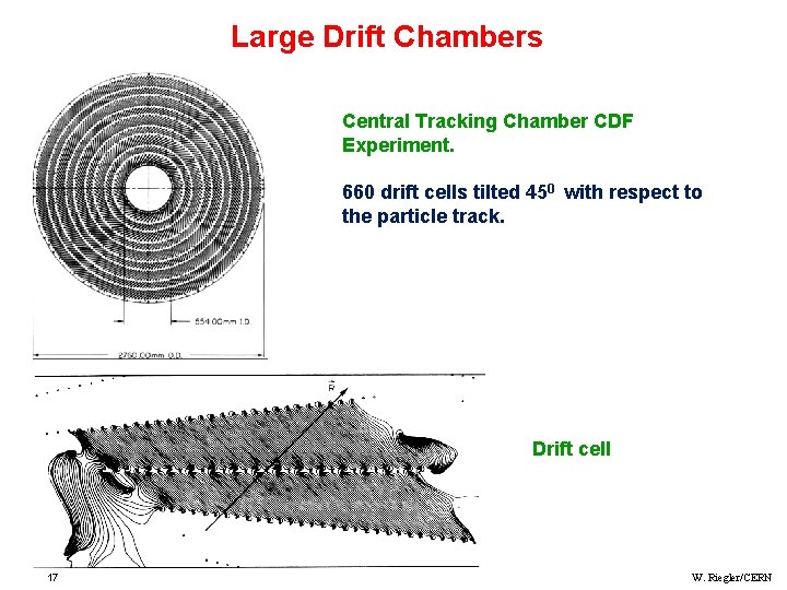
Large Drift Chambers Central Tracking Chamber CDF Experiment. 660 drift cells tilted 450 with respect to the particle track. Drift cell 17 W. Riegler/CERN

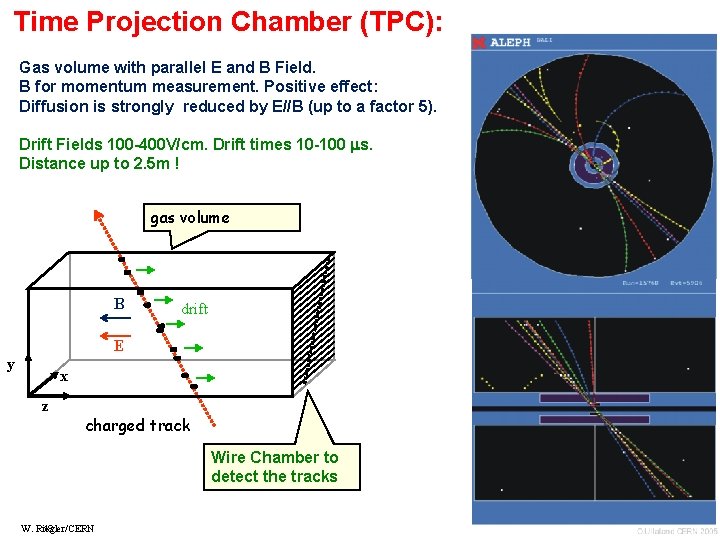
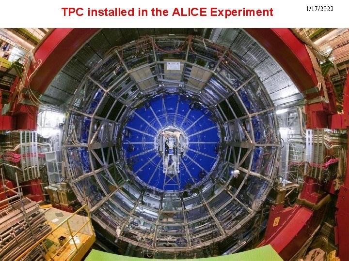
Time Projection Chamber (TPC): Gas volume with parallel E and B Field. B for momentum measurement. Positive effect: Diffusion is strongly reduced by E//B (up to a factor 5). Drift Fields 100 -400 V/cm. Drift times 10 -100 s. Distance up to 2. 5 m ! gas volume B drift E y x z charged track Wire Chamber to detect the tracks W. Riegler/CERN 18

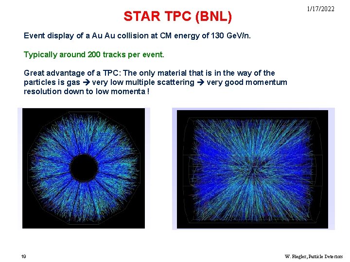
1/17/2022 STAR TPC (BNL) Event display of a Au Au collision at CM energy of 130 Ge. V/n. Typically around 200 tracks per event. Great advantage of a TPC: The only material that is in the way of the particles is gas very low multiple scattering very good momentum resolution down to low momenta ! 19 W. Riegler, Particle Detectors

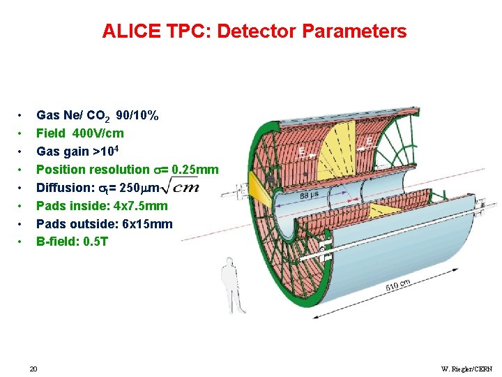
ALICE TPC: Detector Parameters • • Gas Ne/ CO 2 90/10% Field 400 V/cm Gas gain >104 Position resolution = 0. 25 mm Diffusion: t= 250 m Pads inside: 4 x 7. 5 mm Pads outside: 6 x 15 mm B-field: 0. 5 T 20 W. Riegler/CERN

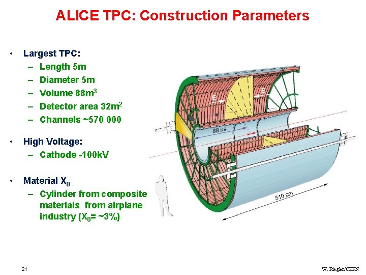
ALICE TPC: Construction Parameters • Largest TPC: – Length 5 m – Diameter 5 m – Volume 88 m 3 – Detector area 32 m 2 – Channels ~570 000 • High Voltage: – Cathode -100 k. V • Material X 0 – Cylinder from composite materials from airplane industry (X 0= ~3%) 21 W. Riegler/CERN

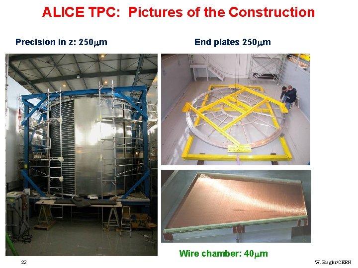
ALICE TPC: Pictures of the Construction Precision in z: 250 m End plates 250 m Wire chamber: 40 m 22 W. Riegler/CERN

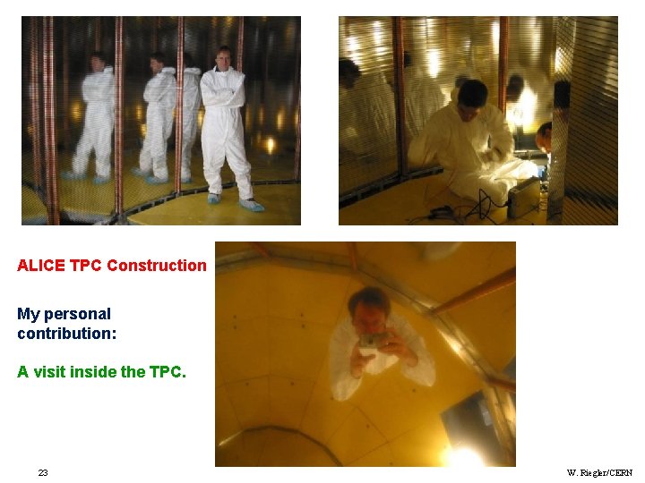
ALICE TPC Construction My personal contribution: A visit inside the TPC. 23 W. Riegler/CERN

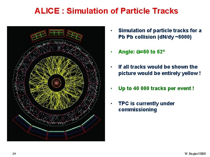
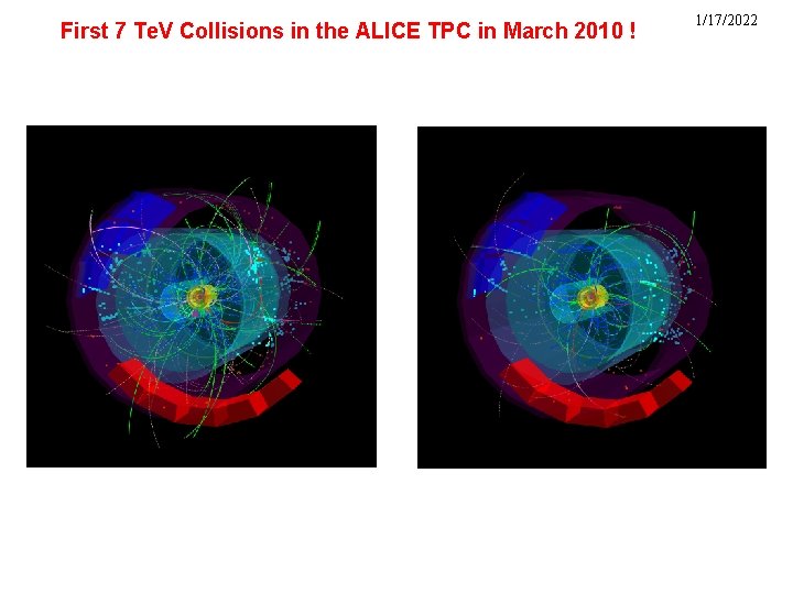
ALICE : Simulation of Particle Tracks 24 • Simulation of particle tracks for a Pb Pb collision (d. N/dy ~8000) • Angle: Q=60 to 62º • If all tracks would be shown the picture would be entirely yellow ! • Up to 40 000 tracks per event ! • TPC is currently under commissioning W. Riegler/CERN

TPC installed in the ALICE Experiment W. Riegler, CERN 1/17/2022

First 7 Te. V Collisions in the ALICE TPC in March 2010 ! 1/17/2022

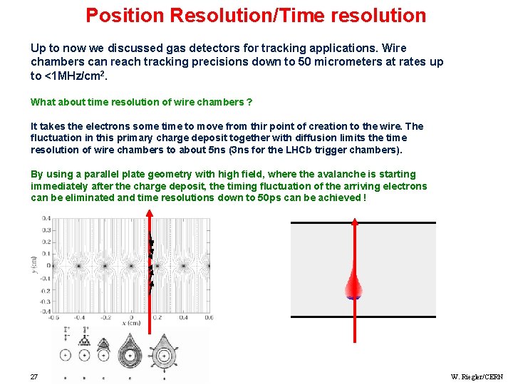
Position Resolution/Time resolution Up to now we discussed gas detectors for tracking applications. Wire chambers can reach tracking precisions down to 50 micrometers at rates up to <1 MHz/cm 2. What about time resolution of wire chambers ? It takes the electrons some time to move from thir point of creation to the wire. The fluctuation in this primary charge deposit together with diffusion limits the time resolution of wire chambers to about 5 ns (3 ns for the LHCb trigger chambers). By using a parallel plate geometry with high field, where the avalanche is starting immediately after the charge deposit, the timing fluctuation of the arriving electrons can be eliminated and time resolutions down to 50 ps can be achieved ! 27 W. Riegler/CERN

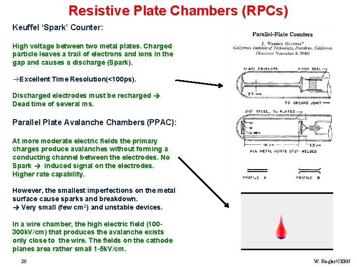
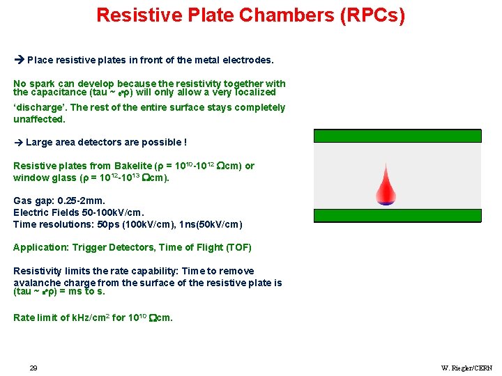
Resistive Plate Chambers (RPCs) Keuffel ‘Spark’ Counter: High voltage between two metal plates. Charged particle leaves a trail of electrons and ions in the gap and causes a discharge (Spark). àExcellent Time Resolution(<100 ps). Discharged electrodes must be recharged Dead time of several ms. Parallel Plate Avalanche Chambers (PPAC): At more moderate electric fields the primary charges produce avalanches without forming a conducting channel between the electrodes. No Spark induced signal on the electrodes. Higher rate capability. However, the smallest imperfections on the metal surface cause sparks and breakdown. Very small (few cm 2) and unstable devices. In a wire chamber, the high electric field (100300 k. V/cm) that produces the avalanche exists only close to the wire. The fields on the cathode planes area rather small 1 -5 k. V/cm. 28 W. Riegler/CERN

Resistive Plate Chambers (RPCs) Place resistive plates in front of the metal electrodes. No spark can develop because the resistivity together with the capacitance (tau ~ e*ρ) will only allow a very localized ‘discharge’. The rest of the entire surface stays completely unaffected. Large area detectors are possible ! Resistive plates from Bakelite (ρ = 1010 -1012 cm) or window glass (ρ = 1012 -1013 cm). Gas gap: 0. 25 -2 mm. Electric Fields 50 -100 k. V/cm. Time resolutions: 50 ps (100 k. V/cm), 1 ns(50 k. V/cm) Application: Trigger Detectors, Time of Flight (TOF) Resistivity limits the rate capability: Time to remove avalanche charge from the surface of the resistive plate is (tau ~ e*ρ) = ms to s. Rate limit of k. Hz/cm 2 for 1010 cm. 29 W. Riegler/CERN

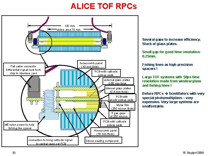
ALICE TOF RPCs 130 mm active area 70 mm Several gaps to increase efficiency. Stack of glass plates. Small gap for good time resolution: 0. 25 mm. Flat cable connector Differential signal sent from strip to interface card honeycomb panel (10 mm thick) PCB with cathode pickup pads external glass plates 0. 55 mm thick internal glass plates (0. 4 mm thick) PCB with anode pickup pads Mylar film (250 micron thick) Fishing lines as high precision spacers ! Large TOF systems with 50 ps time resolution made from window glass and fishing lines ! Before RPCs Scintillators with very special photomultipliers – very expensive. Very large systems are unaffordable. 5 gas gaps of 250 micron M 5 nylon screw to hold fishing-line spacer connection to bring cathode signal to central read-out PCB 30 PCB with cathode pickup pads Honeycomb panel (10 mm thick) Silicon sealing compound W. Riegler/CERN

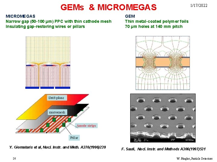
GEMs & MICROMEGAS Narrow gap (50 -100 µm) PPC with thin cathode mesh Insulating gap-restoring wires or pillars Y. Giomataris et al, Nucl. Instr. and Meth. A 376(1996)239 31 1/17/2022 GEM Thin metal-coated polymer foils 70 µm holes at 140 mm pitch F. Sauli, Nucl. Instr. and Methods A 386(1997)531 W. Riegler, Particle Detectors

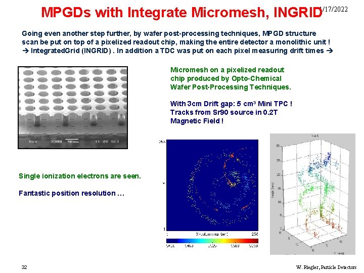
MPGDs with Integrate Micromesh, INGRID 1/17/2022 Going even another step further, by wafer post-processing techniques, MPGD structure scan be put on top of a pixelized readout chip, making the entire detector a monolithic unit ! Integrated. Grid (INGRID). In addition a TDC was put on each pixel measuring drift times Micromesh on a pixelized readout chip produced by Opto-Chemical Wafer Post-Processing Techniques. With 3 cm Drift gap: 5 cm 3 Mini TPC ! Tracks from Sr 90 source in 0. 2 T Magnetic Field ! Single ionization electrons are seen. Fantastic position resolution … 32 W. Riegler, Particle Detectors

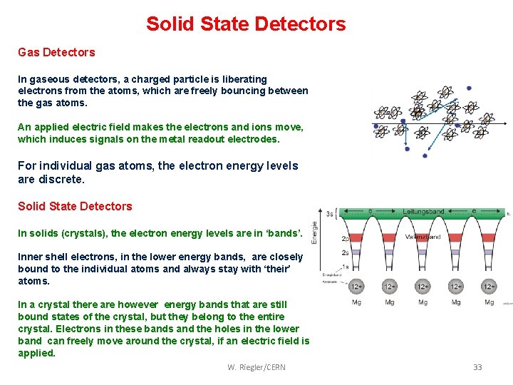
Solid State Detectors Gas Detectors In gaseous detectors, a charged particle is liberating electrons from the atoms, which are freely bouncing between the gas atoms. An applied electric field makes the electrons and ions move, which induces signals on the metal readout electrodes. For individual gas atoms, the electron energy levels are discrete. Solid State Detectors In solids (crystals), the electron energy levels are in ‘bands’. Inner shell electrons, in the lower energy bands, are closely bound to the individual atoms and always stay with ‘their’ atoms. In a crystal there are however energy bands that are still bound states of the crystal, but they belong to the entire crystal. Electrons in these bands and the holes in the lower band can freely move around the crystal, if an electric field is applied. W. Riegler/CERN 33

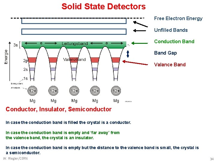
Solid State Detectors Free Electron Energy Unfilled Bands Conduction Band Gap Valance Band Conductor, Insulator, Semiconductor In case the conduction band is filled the crystal is a conductor. In case the conduction band is empty and ‘far away’ from the valence band, the crystal is an insulator. In case the conduction band is empty but the distance to the valence band is small, the crystal is a semiconductor. W. Riegler/CERN 34

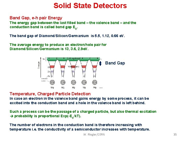
Solid State Detectors Band Gap, e-h pair Energy The energy gap between the last filled band – the valence band – and the conduction band is called band gap Eg. The band gap of Diamond/Silicon/Germanium is 5. 5, 1. 12, 0. 66 e. V. The average energy to produce an electron/hole pair for Diamond/Silicon/Germanium is 13, 3. 6, 2. 9 e. V. Band Gap Temperature, Charged Particle Detection In case an electron in the valence band gains energy by some process, it can be excited into the conduction band a hole in the valence band is left behind. Such a process can be the passage of a charged particle, but also thermal excitation probability is proportional Exp(-Eg/k. T). The number of electrons in the conduction band is therefore increasing with temperature i. e. the conductivity of a semiconductor increases with temperature. W. Riegler/CERN 35

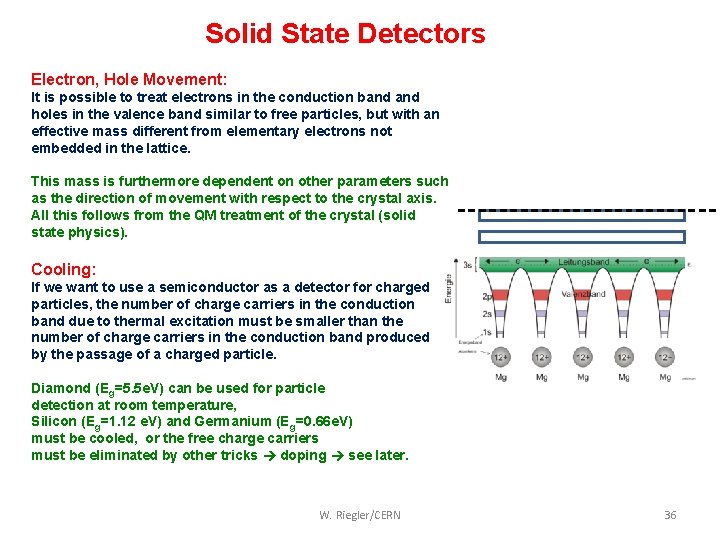
Solid State Detectors Electron, Hole Movement: It is possible to treat electrons in the conduction band holes in the valence band similar to free particles, but with an effective mass different from elementary electrons not embedded in the lattice. This mass is furthermore dependent on other parameters such as the direction of movement with respect to the crystal axis. All this follows from the QM treatment of the crystal (solid state physics). Cooling: If we want to use a semiconductor as a detector for charged particles, the number of charge carriers in the conduction band due to thermal excitation must be smaller than the number of charge carriers in the conduction band produced by the passage of a charged particle. Diamond (Eg=5. 5 e. V) can be used for particle detection at room temperature, Silicon (Eg=1. 12 e. V) and Germanium (Eg=0. 66 e. V) must be cooled, or the free charge carriers must be eliminated by other tricks doping see later. W. Riegler/CERN 36

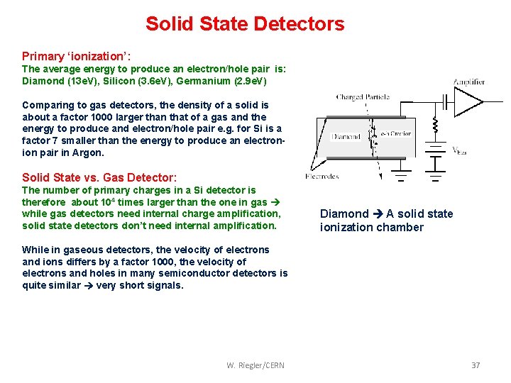
Solid State Detectors Primary ‘ionization’: The average energy to produce an electron/hole pair is: Diamond (13 e. V), Silicon (3. 6 e. V), Germanium (2. 9 e. V) Comparing to gas detectors, the density of a solid is about a factor 1000 larger than that of a gas and the energy to produce and electron/hole pair e. g. for Si is a factor 7 smaller than the energy to produce an electronion pair in Argon. Solid State vs. Gas Detector: The number of primary charges in a Si detector is therefore about 104 times larger than the one in gas while gas detectors need internal charge amplification, solid state detectors don’t need internal amplification. Diamond A solid state ionization chamber While in gaseous detectors, the velocity of electrons and ions differs by a factor 1000, the velocity of electrons and holes in many semiconductor detectors is quite similar very short signals. W. Riegler/CERN 37

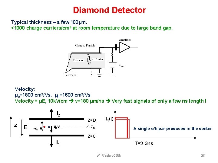
Diamond Detector Typical thickness – a few 100μm. <1000 charge carriers/cm 3 at room temperature due to large band gap. Velocity: μe=1800 cm 2/Vs, μh=1600 cm 2/Vs Velocity = μE, 10 k. V/cm v=180 μm/ns Very fast signals of only a few ns length ! I 2 z E -q, ve q, vh Z=D Z=z 0 I 1(t) A single e/h par produced in the center Z=0 I 1 T=2 -3 ns W. Riegler/CERN 38

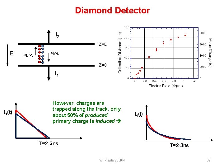
Diamond Detector I 2 Z=D E -q, ve q, vh Z=0 I 1(t) However, charges are trapped along the track, only about 50% of produced primary charge is induced T=2 -3 ns I 1(t) T=2 -3 ns W. Riegler/CERN 39

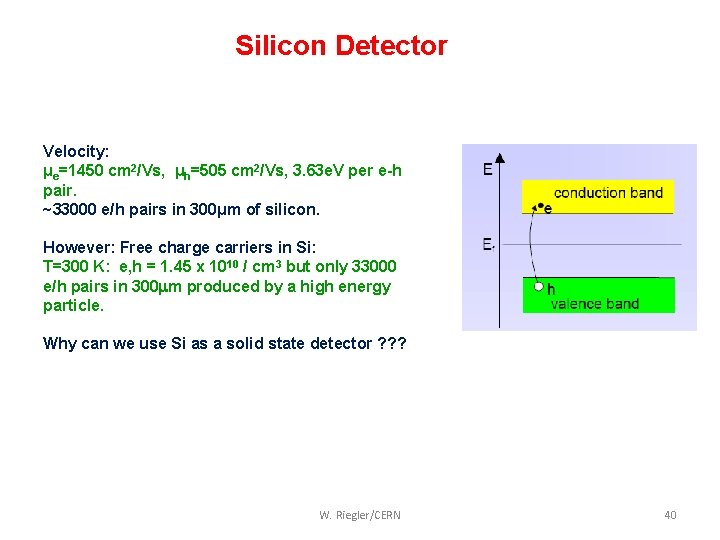
Silicon Detector Velocity: μe=1450 cm 2/Vs, μh=505 cm 2/Vs, 3. 63 e. V per e-h pair. ~33000 e/h pairs in 300μm of silicon. However: Free charge carriers in Si: T=300 K: e, h = 1. 45 x 1010 / cm 3 but only 33000 e/h pairs in 300 m produced by a high energy particle. Why can we use Si as a solid state detector ? ? ? W. Riegler/CERN 40

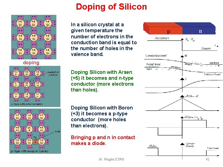
Doping of Silicon In a silicon crystal at a given temperature the number of electrons in the conduction band is equal to the number of holes in the valence band. p n doping Doping Silicon with Arsen (+5) it becomes and n-type conductor (more electrons than holes). Doping Silicon with Boron (+3) it becomes a p-type conductor (more holes than electrons). Bringing p and n in contact makes a diode. W. Riegler/CERN 41

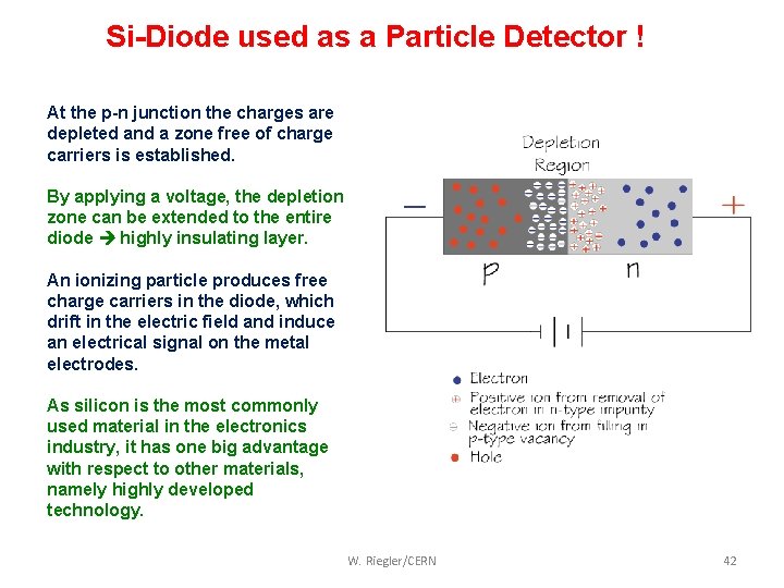
Si-Diode used as a Particle Detector ! At the p-n junction the charges are depleted and a zone free of charge carriers is established. By applying a voltage, the depletion zone can be extended to the entire diode highly insulating layer. An ionizing particle produces free charge carriers in the diode, which drift in the electric field and induce an electrical signal on the metal electrodes. As silicon is the most commonly used material in the electronics industry, it has one big advantage with respect to other materials, namely highly developed technology. W. Riegler/CERN 42

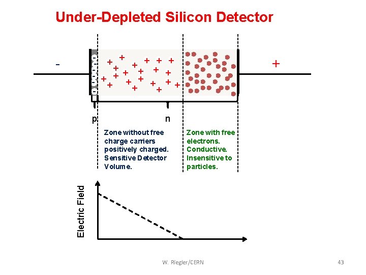
Under-Depleted Silicon Detector + - ++ + + + - + + + - - p + n Zone with free electrons. Conductive. Insensitive to particles. Electric Field Zone without free charge carriers positively charged. Sensitive Detector Volume. W. Riegler/CERN 43

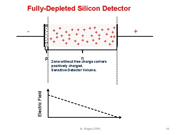
Fully-Depleted Silicon Detector + + + - ++ + + ++ - + + + + - - n Zone without free charge carriers positively charged. Sensitive Detector Volume. Electric Field p + W. Riegler/CERN 44

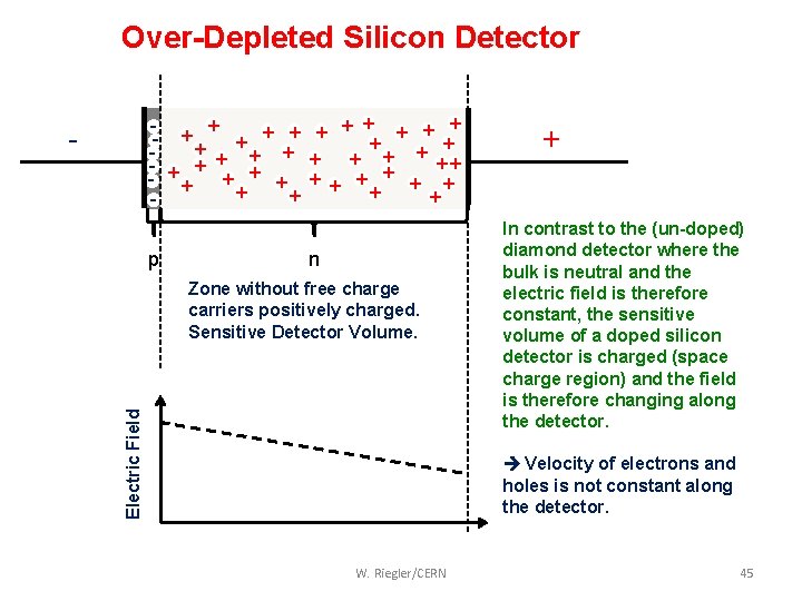
Over-Depleted Silicon Detector + + + - ++ + + ++ - + + + + - - p n Electric Field Zone without free charge carriers positively charged. Sensitive Detector Volume. + In contrast to the (un-doped) diamond detector where the bulk is neutral and the electric field is therefore constant, the sensitive volume of a doped silicon detector is charged (space charge region) and the field is therefore changing along the detector. Velocity of electrons and holes is not constant along the detector. W. Riegler/CERN 45

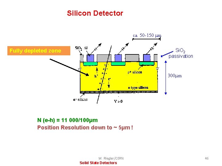
Silicon Detector ca. 50 -150 mm readout capacitances Si. O 2 passivation Fully depleted zone 300 mm N (e-h) = 11 000/100μm Position Resolution down to ~ 5μm ! W. Riegler/CERN Solid State Detectors 46

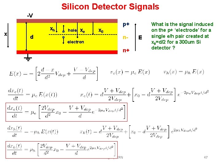
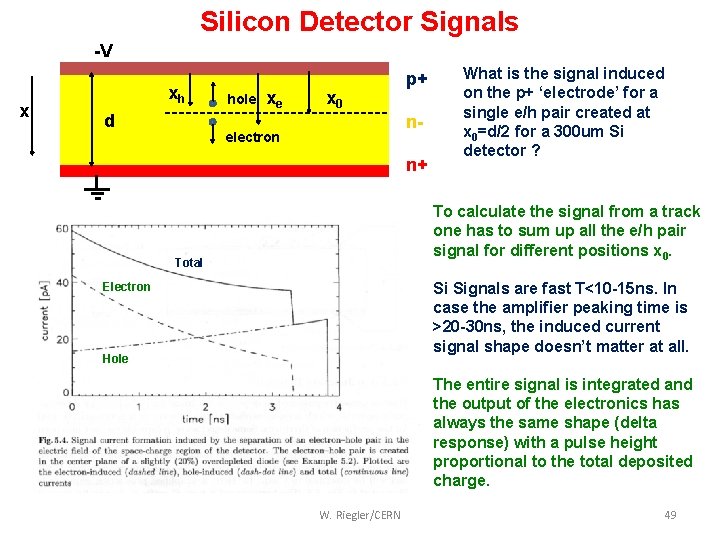
Silicon Detector Signals -V x xh d hole xe electron x 0 p+ nn+ W. Riegler/CERN E What is the signal induced on the p+ ‘electrode’ for a single e/h pair created at x 0=d/2 for a 300 um Si detector ? 47

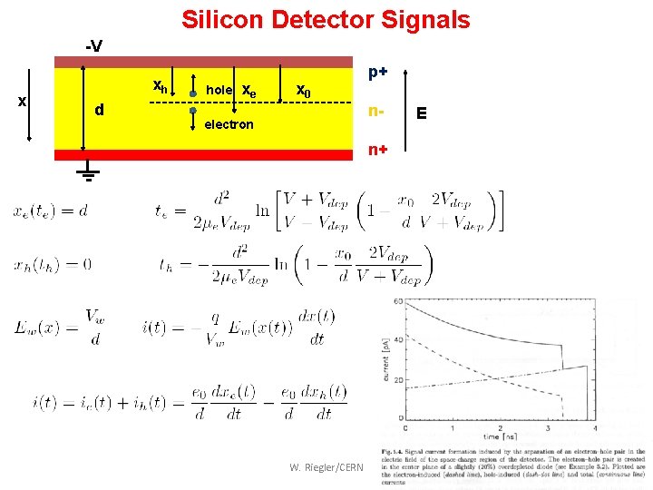
Silicon Detector Signals -V x xh d hole xe x 0 p+ n- electron E n+ W. Riegler/CERN 48

Silicon Detector Signals -V x xh d hole xe x 0 p+ n- electron n+ What is the signal induced on the p+ ‘electrode’ for a single e/h pair created at x 0=d/2 for a 300 um Si detector ? To calculate the signal from a track one has to sum up all the e/h pair signal for different positions x 0. Total Si Signals are fast T<10 -15 ns. In case the amplifier peaking time is >20 -30 ns, the induced current signal shape doesn’t matter at all. Electron Hole The entire signal is integrated and the output of the electronics has always the same shape (delta response) with a pulse height proportional to the total deposited charge. W. Riegler/CERN 49

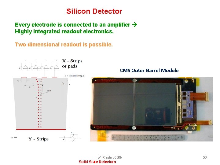
Silicon Detector Every electrode is connected to an amplifier Highly integrated readout electronics. Two dimensional readout is possible. CMS Outer Barrel Module W. Riegler/CERN Solid State Detectors 50

W. Riegler/CERN 51

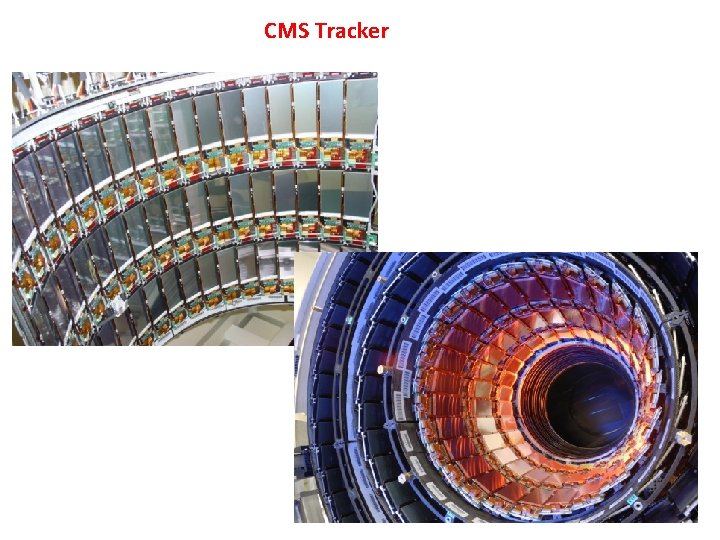
CMS Tracker W. Riegler/CERN 52

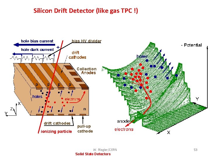
Silicon Drift Detector (like gas TPC !) bias HV divider Collection drift cathodes ionizing particle pull-up cathode W. Riegler/CERN Solid State Detectors 53

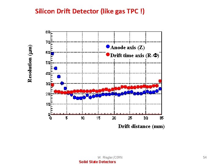
Resolution ( m) Silicon Drift Detector (like gas TPC !) ·Anode axis (Z) ·Drift time axis (R-F) Drift distance (mm) W. Riegler/CERN Solid State Detectors 54

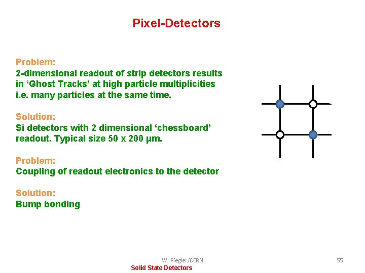
Pixel-Detectors Problem: 2 -dimensional readout of strip detectors results in ‘Ghost Tracks’ at high particle multiplicities i. e. many particles at the same time. Solution: Si detectors with 2 dimensional ‘chessboard’ readout. Typical size 50 x 200 μm. Problem: Coupling of readout electronics to the detector Solution: Bump bonding W. Riegler/CERN Solid State Detectors 55

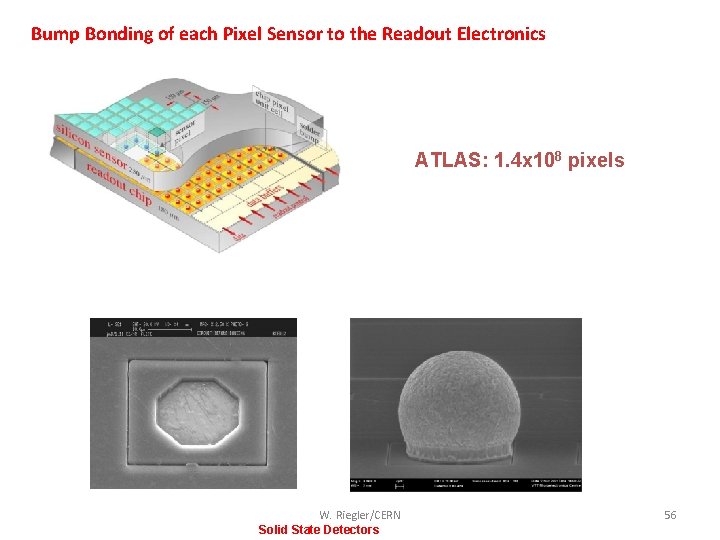
Bump Bonding of each Pixel Sensor to the Readout Electronics ATLAS: 1. 4 x 108 pixels W. Riegler/CERN Solid State Detectors 56

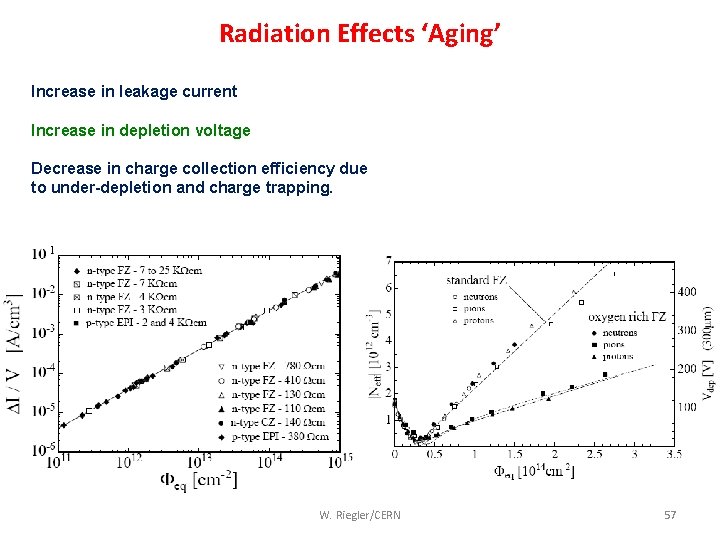
Radiation Effects ‘Aging’ Increase in leakage current Increase in depletion voltage Decrease in charge collection efficiency due to under-depletion and charge trapping. W. Riegler/CERN 57

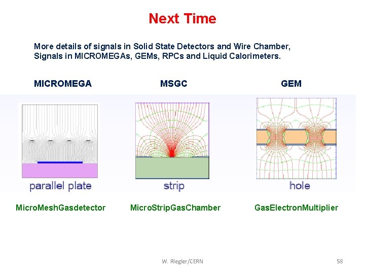
Next Time More details of signals in Solid State Detectors and Wire Chamber, Signals in MICROMEGAs, GEMs, RPCs and Liquid Calorimeters. MICROMEGA MSGC Micro. Mesh. Gasdetector Micro. Strip. Gas. Chamber W. Riegler/CERN GEM Gas. Electron. Multiplier 58

Conclusion This principle of signal generation is identical for Solid State Detectors, Gas Detectors and Liquid Detectors. The signals are due to charges (currents) induced on metal electrodes by moving charges. The easiest way to calculate signals induced by moving charges on metal electrodes is the use of Weighting fields (Ramo – Shockley theorem) for calculation of currents induced on grounded electrodes. These currents can then be placed as ideal current sources on an equivalent circuit diagram representing the detector. 1/17/2022 W. Riegler, Particle Detectors 59