Sierra Proto Express Introducing our Micro Electronics Division

- Slides: 22

Sierra Proto Express Introducing our Micro Electronics Division

Sierra Proto Express PCBs for MICROELECTRONICS Design For Manufacturability Presented by Ken Bahl President, Sierra Proto Express at PCB Design West Conference March 2006 Santa Clara, CA (these slides have been slightly modified for web download) 2/28/2021 Copyright Sierra Proto Express 2006

Presented at Sierra Proto Express PCB Design West Conference Santa Clara, CA, March 2006 2/28/2021 Copyright Sierra Proto Express 2006

Sierra Proto Express What are Microelectronics PCBs? ü Microelectronics PCBs generally refers to circuit boards with less than 2 Mil (0. 002”) Lines and Spaces. ü These are very tight, small boards which serve the rapidly growing microelectronics market, whose end products include applications like cell phones, PDAs, and personal game machines. Conventional PCBs with 4 mil or more trace/space are just not suitable for the increasing complexity and decreasing form factors of the devices of tomorrow. 2/28/2021 Copyright Sierra Proto Express 2006

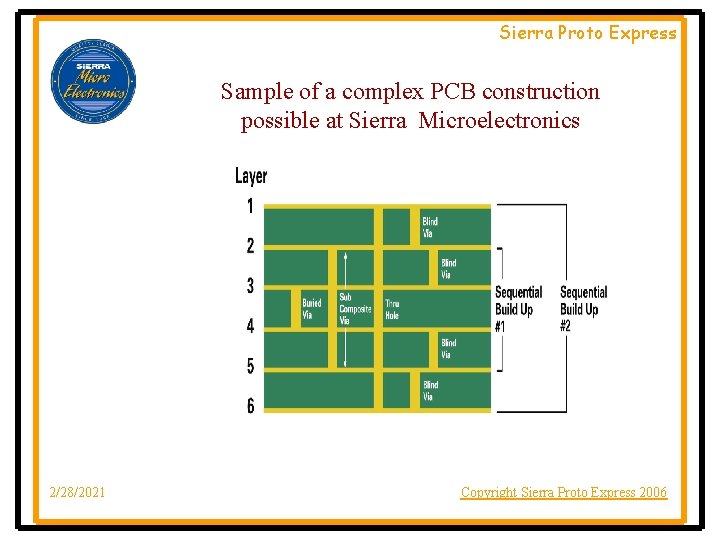
Sierra Proto Express We can produce Microelectronic PCBs with following Construction Types ü Single sided ü Double sided ü Multilayer sequential build up ü Blind via ü Buried via ü Sub-Composite Via 2/28/2021 Copyright Sierra Proto Express 2006

Sierra Proto Express We use the following Laminate Material Types ü High Temp Lead-free (IS 410 or equivalent) ü Polyimide ü BT ü Low Dk/Df (N 4000 -13 or equivalent) ü Standard FR 4 2/28/2021 Copyright Sierra Proto Express 2006

Sierra Proto Express Design Guidelines: Minimum Line and Space ü Minimum line of 0. 00125” ü Minimum space of 0. 00125” ü If conflict, reduce line-width, but must maintain minimum space 2/28/2021 Copyright Sierra Proto Express 2006

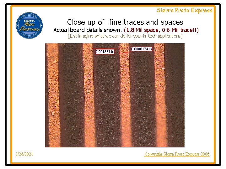
Sierra Proto Express Close up of fine traces and spaces Actual board details shown. (1. 8 Mil space, 0. 6 Mil trace!!) [just imagine what we can do for your hi tech applications] 2/28/2021 Copyright Sierra Proto Express 2006

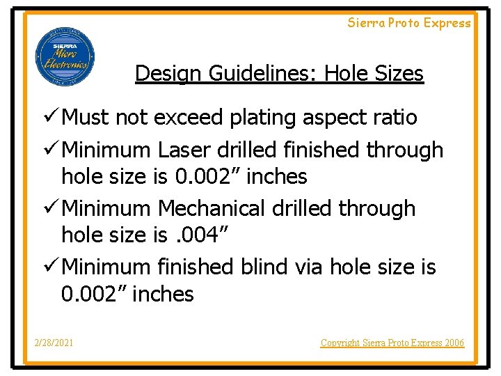
Sierra Proto Express Design Guidelines: Hole Sizes ü Must not exceed plating aspect ratio ü Minimum Laser drilled finished through hole size is 0. 002” inches ü Minimum Mechanical drilled through hole size is. 004” ü Minimum finished blind via hole size is 0. 002” inches 2/28/2021 Copyright Sierra Proto Express 2006

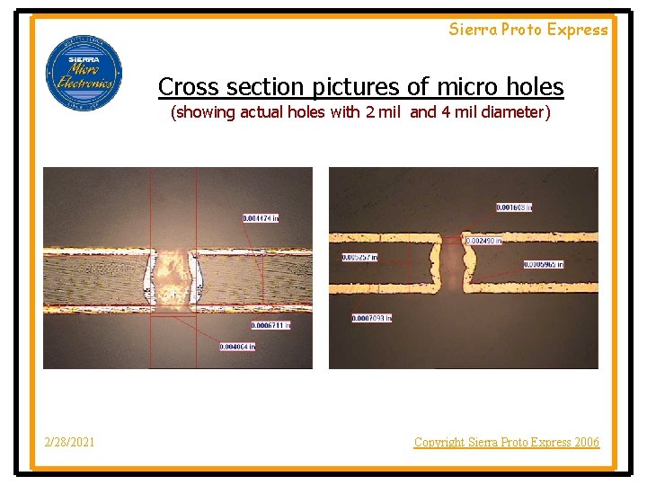
Sierra Proto Express Cross section pictures of micro holes (showing actual holes with 2 mil and 4 mil diameter) 2/28/2021 Copyright Sierra Proto Express 2006

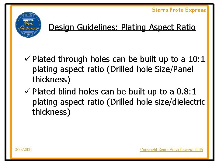
Sierra Proto Express Design Guidelines: Plating Aspect Ratio ü Plated through holes can be built up to a 10: 1 plating aspect ratio (Drilled hole Size/Panel thickness) ü Plated blind holes can be built up to a 0. 8: 1 plating aspect ratio (Drilled hole size/dielectric thickness) 2/28/2021 Copyright Sierra Proto Express 2006

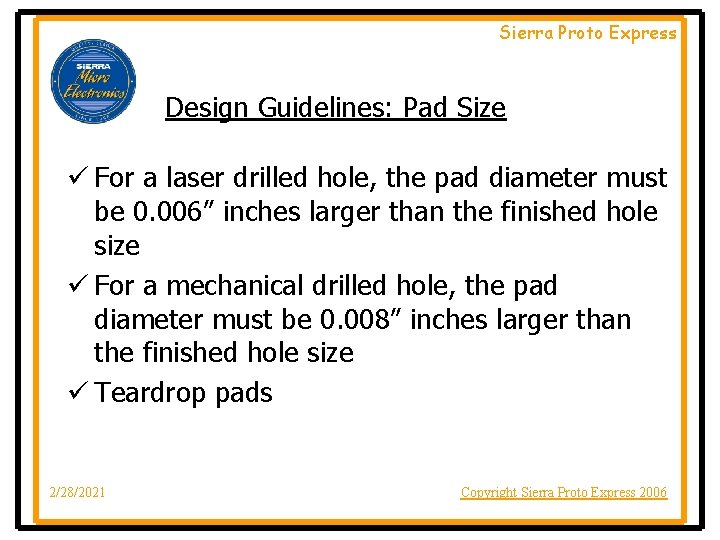
Sierra Proto Express Design Guidelines: Pad Size ü For a laser drilled hole, the pad diameter must be 0. 006” inches larger than the finished hole size ü For a mechanical drilled hole, the pad diameter must be 0. 008” inches larger than the finished hole size ü Teardrop pads 2/28/2021 Copyright Sierra Proto Express 2006

Sierra Proto Express Design Guidelines: Copper Thickness ü Total copper thickness in the hole – Minimum of 0. 0005” inches – Maximum of 0. 0008” inches ü Total copper thickness on the surface – Minimum of 0. 0005” inches – Maximum of 0. 0008” inches 2/28/2021 Copyright Sierra Proto Express 2006

Sierra Proto Express Design Guidelines: Surface Finishes ü Solder mask over bare copper (SMOBC) ü ENIG (Electroless Nickel Immersion Gold) ü Immersion Silver ü Entek OSP (Organic Surface Protection) 2/28/2021 Copyright Sierra Proto Express 2006

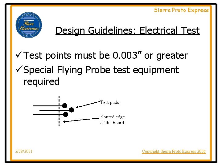
Sierra Proto Express Design Guidelines: Electrical Test ü Test points must be 0. 003” or greater ü Special Flying Probe test equipment required Test pads Routed edge of the board 2/28/2021 Copyright Sierra Proto Express 2006

Sierra Proto Express Design Guidelines: Finished Board Thickness ü Must not violate plating aspect ratio ü Minimum core thickness of 0. 0025” ü Minimum Dielectric is. 002” ü Maximum finished board of 0. 062” ü All materials are made in-house 2/28/2021 Copyright Sierra Proto Express 2006

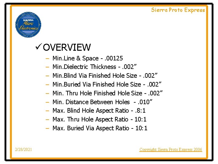
Sierra Proto Express ü OVERVIEW – – – – – 2/28/2021 Min. Line & Space -. 00125 Min. Dielectric Thickness -. 002” Min. Blind Via Finished Hole Size -. 002” Min. Buried Via Finished Hole Size -. 002” Min. Thru Hole Finished Hole Size -. 002” Min. Distance Between Holes -. 010” Max. Blind Hole Aspect Ratio -. 8: 1 Max. Thru Hole Aspect Ratio - 10: 1 Max. Buried Via Aspect Ratio - 10: 1 Copyright Sierra Proto Express 2006

Sierra Proto Express Sample of a complex PCB construction possible at Sierra Microelectronics 2/28/2021 Copyright Sierra Proto Express 2006

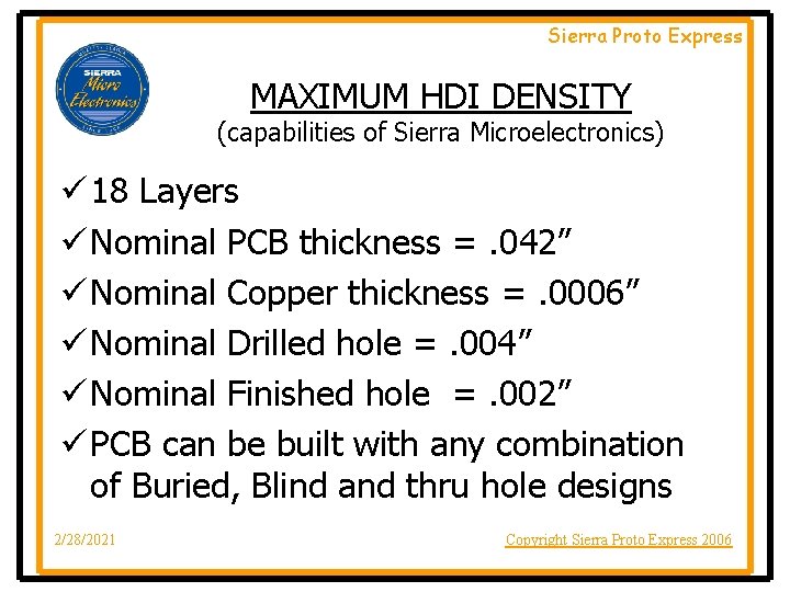
Sierra Proto Express MAXIMUM HDI DENSITY (capabilities of Sierra Microelectronics) ü 18 Layers ü Nominal PCB thickness =. 042” ü Nominal Copper thickness =. 0006” ü Nominal Drilled hole =. 004” ü Nominal Finished hole =. 002” ü PCB can be built with any combination of Buried, Blind and thru hole designs 2/28/2021 Copyright Sierra Proto Express 2006

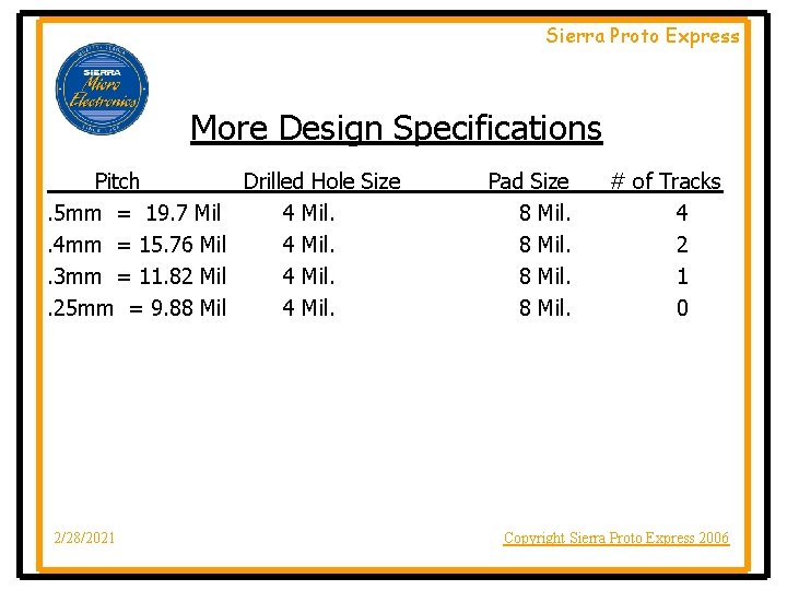
Sierra Proto Express More Design Specifications Pitch Drilled Hole Size. 5 mm = 19. 7 Mil 4 Mil. . 4 mm = 15. 76 Mil 4 Mil. . 3 mm = 11. 82 Mil 4 Mil. . 25 mm = 9. 88 Mil 4 Mil. 2/28/2021 Pad Size 8 Mil. # of Tracks 4 2 1 0 Copyright Sierra Proto Express 2006

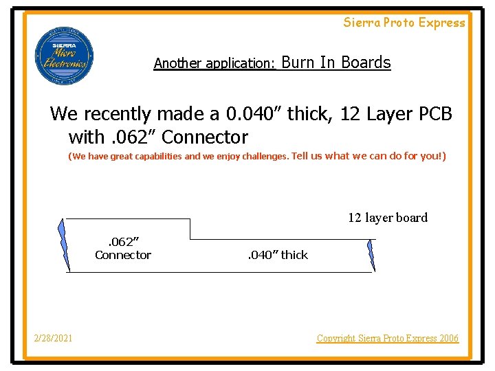
Sierra Proto Express Another application: Burn In Boards We recently made a 0. 040” thick, 12 Layer PCB with. 062” Connector (We have great capabilities and we enjoy challenges. Tell us what we can do for you!) 12 layer board. 062” Connector 2/28/2021 . 040” thick Copyright Sierra Proto Express 2006

Sierra Proto Express Think of us as your PCB partner in the exciting new world of Micro Electronics For more details visit: www. protoexpress. com/microelectronics Contact Ken Bahl ken@protoexpress. com Or leave a message for Ken at (408) 735 -7137 X 9934 2/28/2021 Copyright Sierra Proto Express 2006