Sharif Digital Flow Introduction Part I Synthesize Power
![Clock Gating Command set_clock_gating_style [-sequential_celllatch | none] [-minimum_bitwidth_value] [-setup_value] [-hold_value] [-positive_edge_logic{ gate_list | integrated}] Clock Gating Command set_clock_gating_style [-sequential_celllatch | none] [-minimum_bitwidth_value] [-setup_value] [-hold_value] [-positive_edge_logic{ gate_list | integrated}]](https://slidetodoc.com/presentation_image/56fc45fdb9928e139eac2e2bf0b0be9c/image-45.jpg)




![Sharif Dependable System Lab [DSL] �HSIM were used as part of fault injection flow Sharif Dependable System Lab [DSL] �HSIM were used as part of fault injection flow](https://slidetodoc.com/presentation_image/56fc45fdb9928e139eac2e2bf0b0be9c/image-116.jpg)
![Sharif Dependable System Lab [DSL] 117 Sharif Dependable System Lab [DSL] 117](https://slidetodoc.com/presentation_image/56fc45fdb9928e139eac2e2bf0b0be9c/image-117.jpg)
![Sharif Dependable System Lab [DSL] �With HSIM �We get an accurate simulation of fault, Sharif Dependable System Lab [DSL] �With HSIM �We get an accurate simulation of fault,](https://slidetodoc.com/presentation_image/56fc45fdb9928e139eac2e2bf0b0be9c/image-118.jpg)


- Slides: 128

Sharif Digital Flow Introduction Part I : Synthesize & Power Analyze Nemat Allah Ahmadyan Dependable System Lab [DSL], CE Department Sharif University of technology 2009

Introduction �The following presentation is based on �Version 1. 213 �Mentor Model. Sim 6. 5 SE �Synopsys Design Compiler 2007 �Cadence So. C Encounter 8. 1 �Synopsys HSIM 2007 �Synopsys Prime. Power 2003 �Synopsys Prime. Time 2003 2

© before we begin �Part of these slides are extracted from the following copyrighted materials: �Synopsys Design. Compiler, Power. Compiler & Prime. Power Reference Manual & User guide �ASIC Design Flow Slides, prepared by Frank Gurkayanak �From Integrated Systems Labratoary, EPFL �Cadence So. C Encounter Synthesis Place-and-route flow guide �Synopsys HSIM reference manual. 3

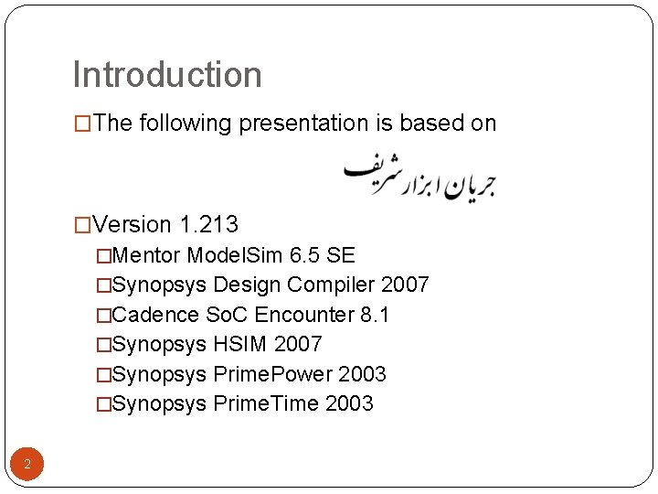
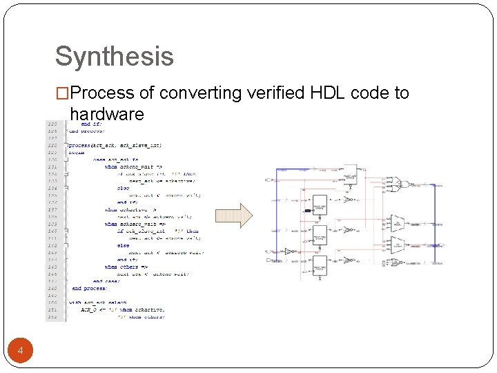
Synthesis �Process of converting verified HDL code to hardware 4

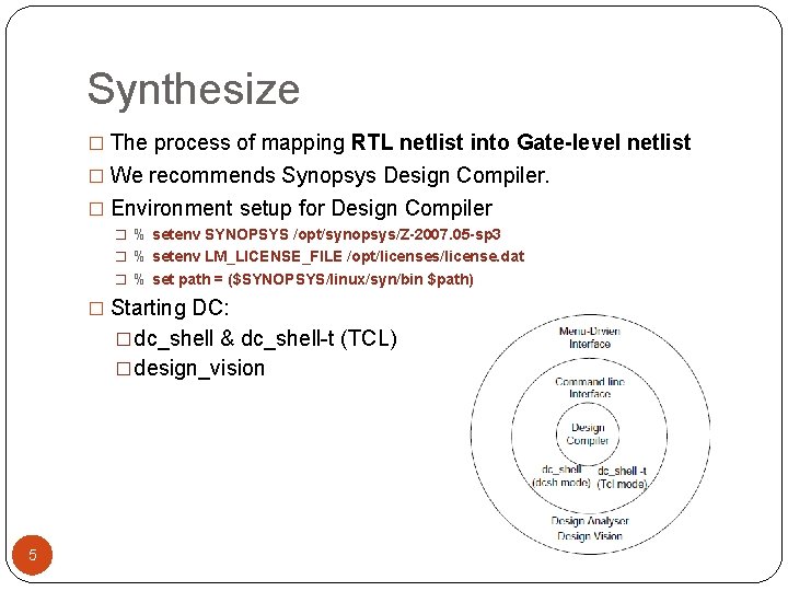
Synthesize � The process of mapping RTL netlist into Gate-level netlist � We recommends Synopsys Design Compiler. � Environment setup for Design Compiler � % setenv SYNOPSYS /opt/synopsys/Z-2007. 05 -sp 3 � % setenv LM_LICENSE_FILE /opt/licenses/license. dat � % set path = ($SYNOPSYS/linux/syn/bin $path) � Starting DC: �dc_shell & dc_shell-t (TCL) �design_vision 5

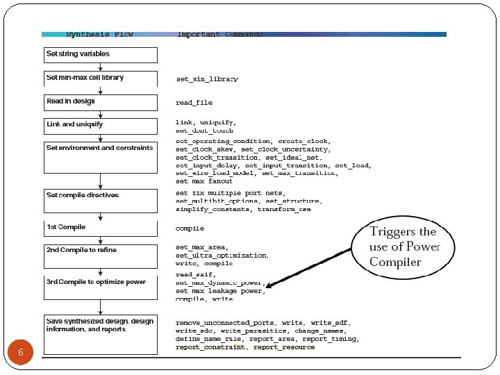
6

Defining Variables �Variables includes: �Libraries (min/max) �Cache �Design �constraints 7

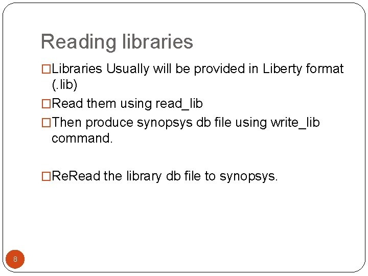
Reading libraries �Libraries Usually will be provided in Liberty format (. lib) �Read them using read_lib �Then produce synopsys db file using write_lib command. �Re. Read the library db file to synopsys. 8

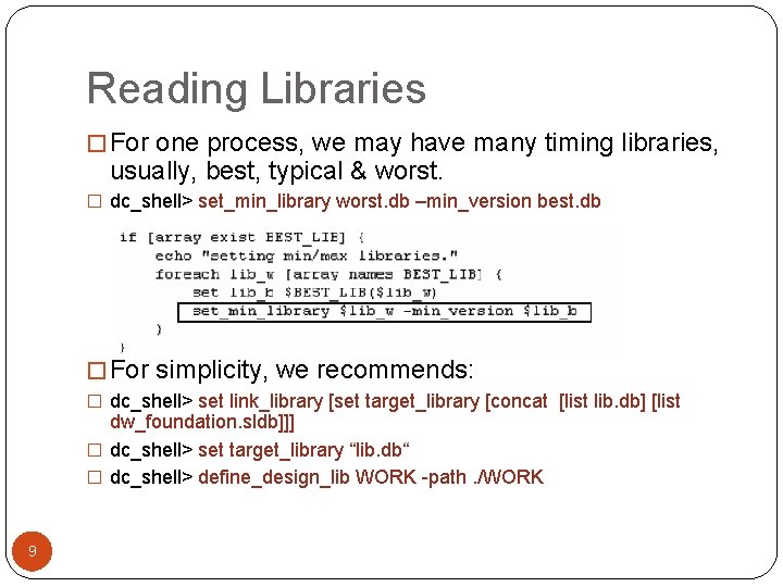
Reading Libraries � For one process, we may have many timing libraries, usually, best, typical & worst. � dc_shell> set_min_library worst. db –min_version best. db � For simplicity, we recommends: � dc_shell> set link_library [set target_library [concat [list lib. db] [list dw_foundation. sldb]]] � dc_shell> set target_library “lib. db“ � dc_shell> define_design_lib WORK -path. /WORK 9

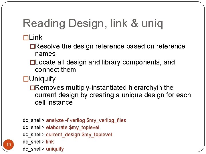
Reading Design, link & uniq �Link �Resolve the design reference based on reference names �Locate all design and library components, and connect them �Uniquify �Removes multiply-instantiated hierarchyin the current design by creating a unique design for each cell instance 10 dc_shell> analyze -f verilog $my_verilog_files dc_shell> elaborate $my_toplevel dc_shell> current_design $my_toplevel dc_shell> link dc_shell> uniquify

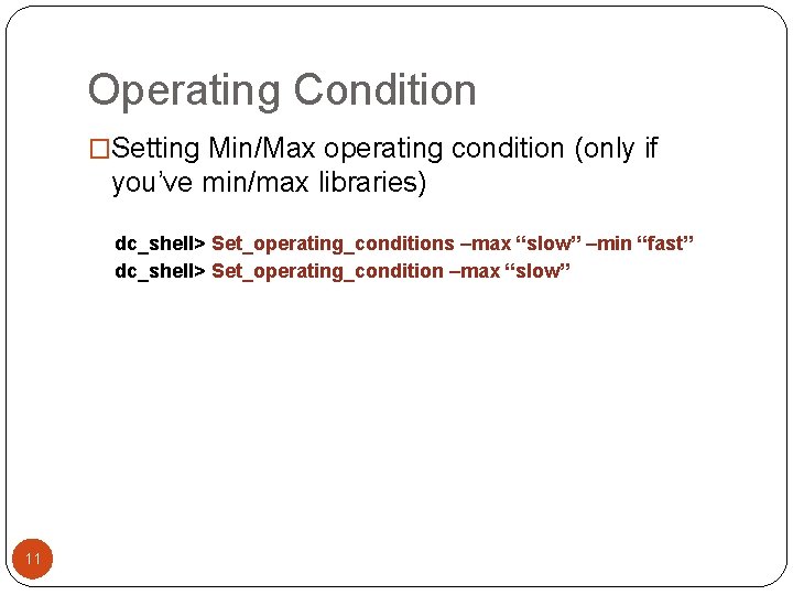
Operating Condition �Setting Min/Max operating condition (only if you’ve min/max libraries) dc_shell> Set_operating_conditions –max “slow” –min “fast” dc_shell> Set_operating_condition –max “slow” 11

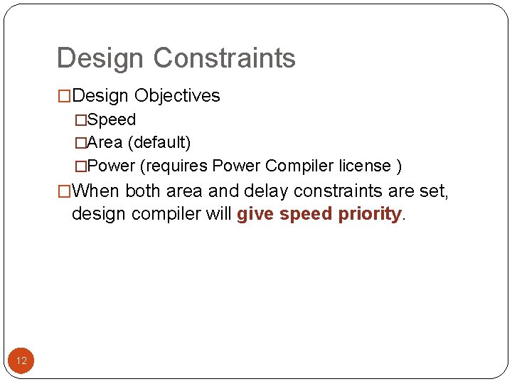
Design Constraints �Design Objectives �Speed �Area (default) �Power (requires Power Compiler license ) �When both area and delay constraints are set, design compiler will give speed priority. 12

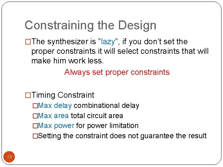
Constraining the Design �The synthesizer is ”lazy”, if you don’t set the proper constraints it will select constraints that will make him work less. Always set proper constraints �Timing Constraint �Max delay combinational delay �Max area total circuit area �Max power for power limitation �Setting the constraint does not guarantee the result 13

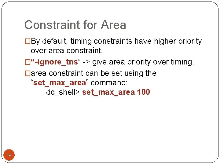
Constraint for Area �By default, timing constraints have higher priority over area constraint. �“-ignore_tns” -> give area priority over timing. �area constraint can be set using the “set_max_area” command: dc_shell> set_max_area 100 14

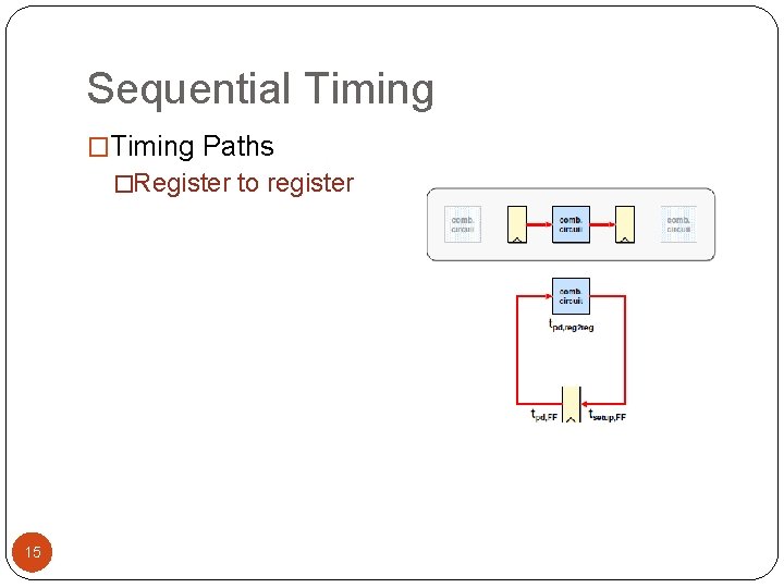
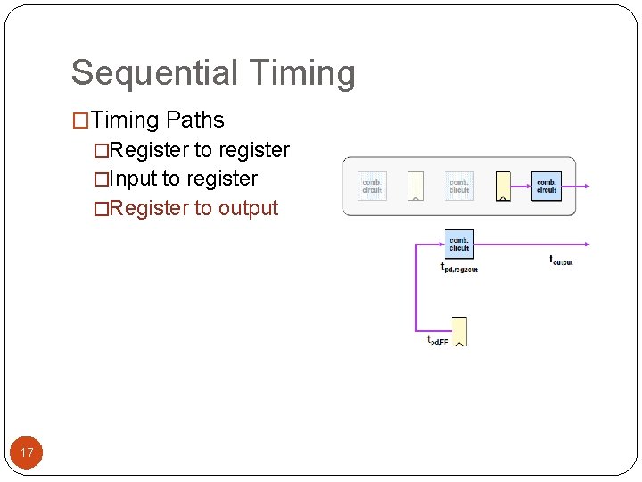
Sequential Timing �Timing Paths �Register to register 15

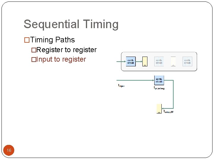
Sequential Timing �Timing Paths �Register to register �Input to register 16

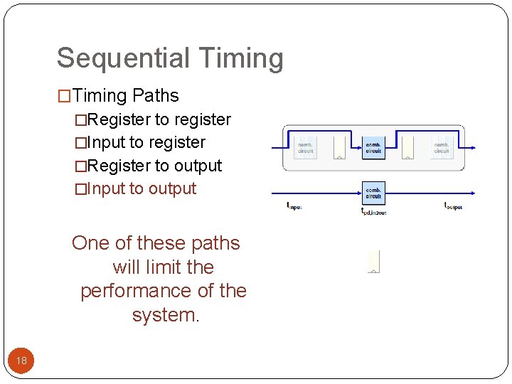
Sequential Timing �Timing Paths �Register to register �Input to register �Register to output 17

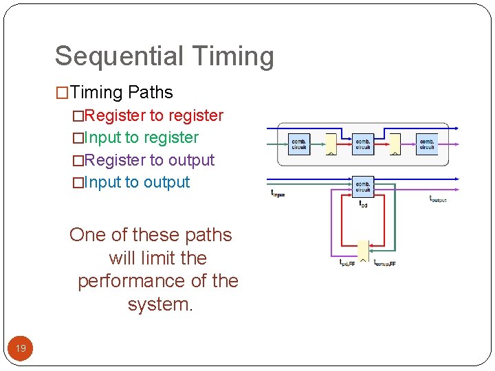
Sequential Timing �Timing Paths �Register to register �Input to register �Register to output �Input to output One of these paths will limit the performance of the system. 18

Sequential Timing �Timing Paths �Register to register �Input to register �Register to output �Input to output One of these paths will limit the performance of the system. 19

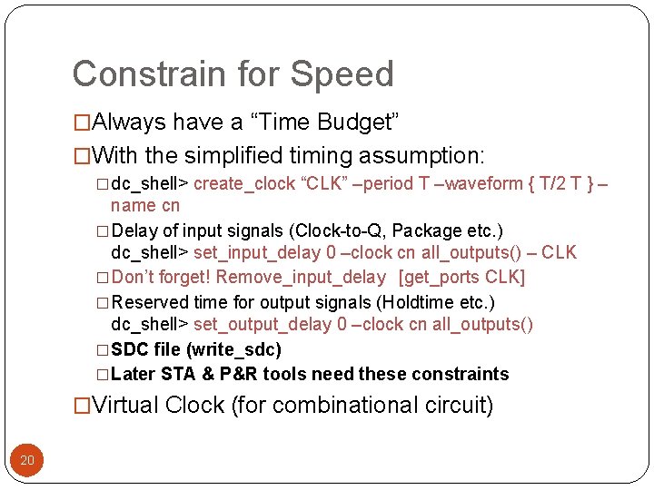
Constrain for Speed �Always have a “Time Budget” �With the simplified timing assumption: �dc_shell> create_clock “CLK” –period T –waveform { T/2 T } – name cn �Delay of input signals (Clock-to-Q, Package etc. ) dc_shell> set_input_delay 0 –clock cn all_outputs() – CLK �Don’t forget! Remove_input_delay [get_ports CLK] �Reserved time for output signals (Holdtime etc. ) dc_shell> set_output_delay 0 –clock cn all_outputs() �SDC file (write_sdc) �Later STA & P&R tools need these constraints �Virtual Clock (for combinational circuit) 20

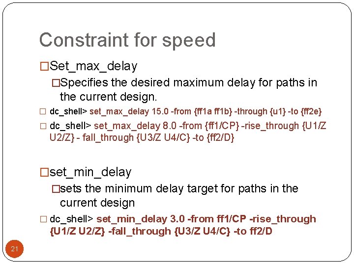
Constraint for speed �Set_max_delay �Specifies the desired maximum delay for paths in the current design. � dc_shell> set_max_delay 15. 0 -from {ff 1 a ff 1 b} -through {u 1} -to {ff 2 e} � dc_shell> set_max_delay 8. 0 -from {ff 1/CP} -rise_through {U 1/Z U 2/Z} - fall_through {U 3/Z U 4/C} -to {ff 2/D} �set_min_delay �sets the minimum delay target for paths in the current design � dc_shell> set_min_delay 3. 0 -from ff 1/CP -rise_through {U 1/Z U 2/Z} -fall_through {U 3/Z U 4/C} -to ff 2/D 21

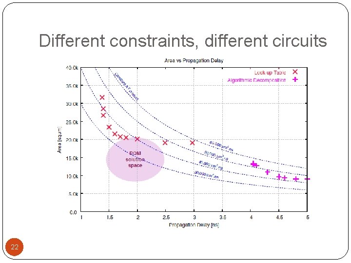
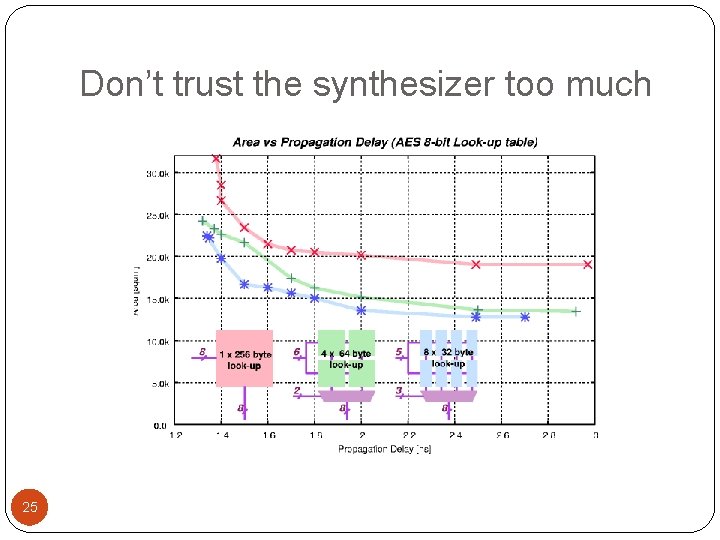
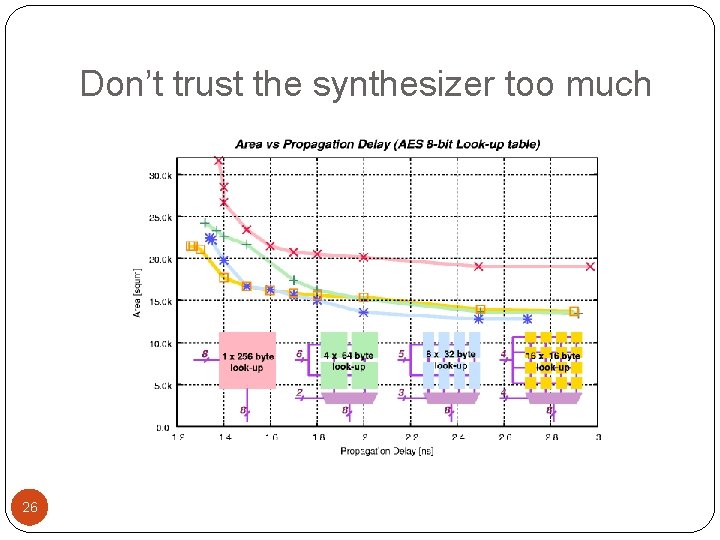
Different constraints, different circuits 22

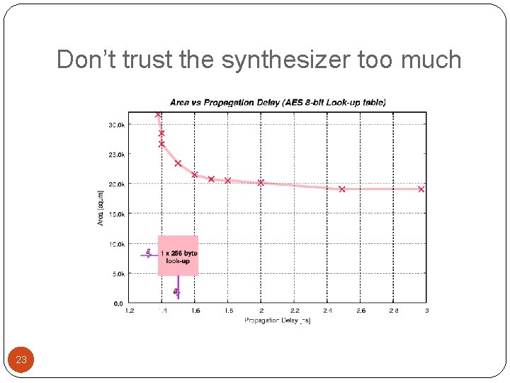
Don’t trust the synthesizer too much 23

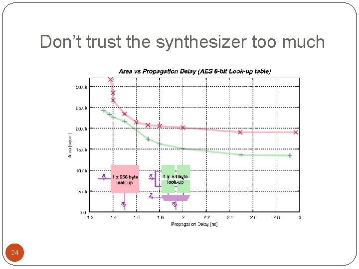
Don’t trust the synthesizer too much 24

Don’t trust the synthesizer too much 25

Don’t trust the synthesizer too much 26

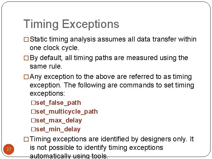
Timing Exceptions � Static timing analysis assumes all data transfer within one clock cycle. � By default, all timing paths are measured using the same rule. � Any exception to the above are referred to as timing exception. The following are commands to set timing exceptions: �set_false_path �set_multicycle_path �set_max_delay �set_min_delay � Timing exceptions are identified by designers only. It 27 is not possible to identify timing exceptions automatically using tools.

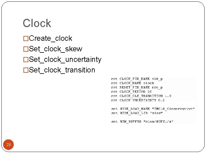
Clock �Create_clock �Set_clock_skew �Set_clock_uncertainty �Set_clock_transition 28

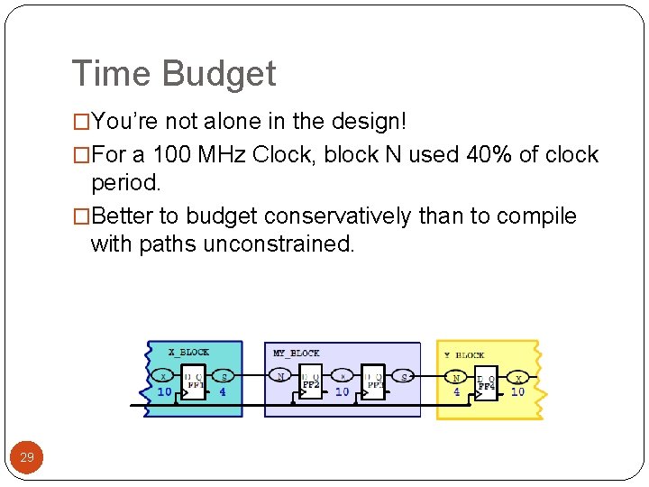
Time Budget �You’re not alone in the design! �For a 100 MHz Clock, block N used 40% of clock period. �Better to budget conservatively than to compile with paths unconstrained. 29

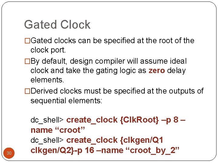
Gated Clock �Gated clocks can be specified at the root of the clock port. �By default, design compiler will assume ideal clock and take the gating logic as zero delay elements. �Derived clocks must be specified at the outputs of sequential elements: dc_shell> create_clock {Clk. Root} –p 8 – 30 name “croot” dc_shell> create_clock {clkgen/Q 1 clkgen/Q 2}-p 16 –name “croot_by_2”

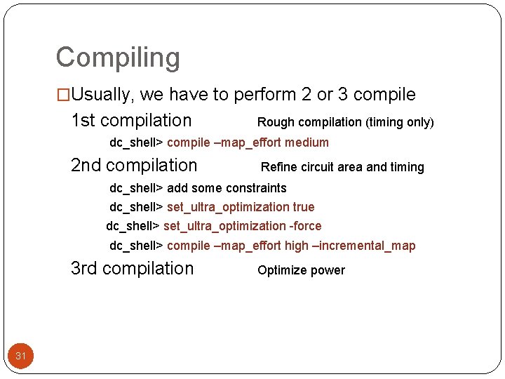
Compiling �Usually, we have to perform 2 or 3 compile 1 st compilation Rough compilation (timing only) dc_shell> compile –map_effort medium 2 nd compilation Refine circuit area and timing dc_shell> add some constraints dc_shell> set_ultra_optimization true dc_shell> set_ultra_optimization -force dc_shell> compile –map_effort high –incremental_map 3 rd compilation 31 Optimize power

Synopsys power compiler Optimize for Power with 32

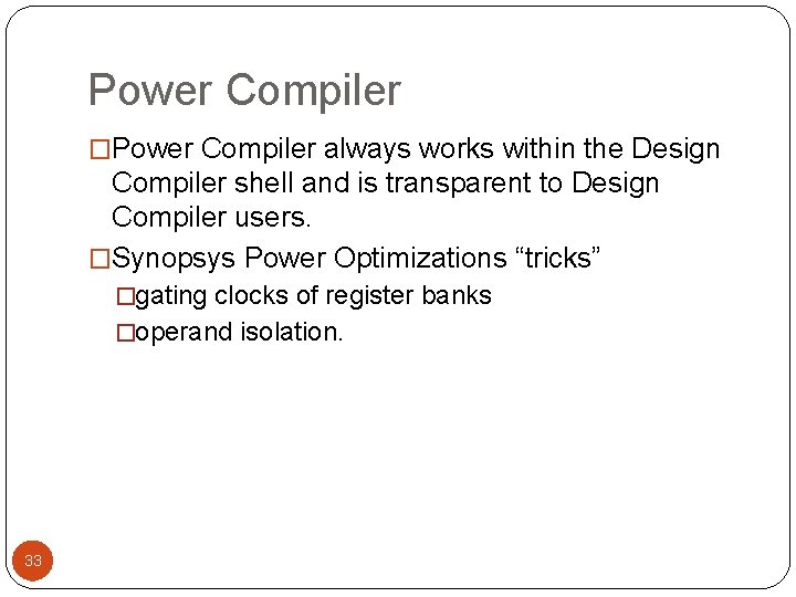
Power Compiler �Power Compiler always works within the Design Compiler shell and is transparent to Design Compiler users. �Synopsys Power Optimizations “tricks” �gating clocks of register banks �operand isolation. 33

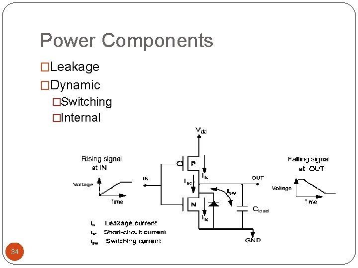
Power Components �Leakage �Dynamic �Switching �Internal 34

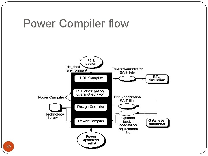
Power Compiler flow 35

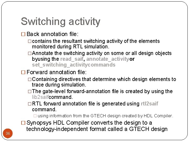
Switching activity � Back annotation file: �contains the resultant switching activity of the elements monitored during RTL simulation. �Annotate the switching activity on some or all design objects byusing the read_saif, annotate_activityor set_switching_activitycommands � Forward annotation file: �Containing directives that determine which design elements to trace during simulation. �The gate-level forward-annotation file is created by using the lib 2 saifcommand. �RTL forward annotation file is generated using rtl 2 saif command. � using information from the GTECH design created by HDL Compiler. � Synopsys HDL Compiler converts the design to a 36 technology-independent format called a GTECH design

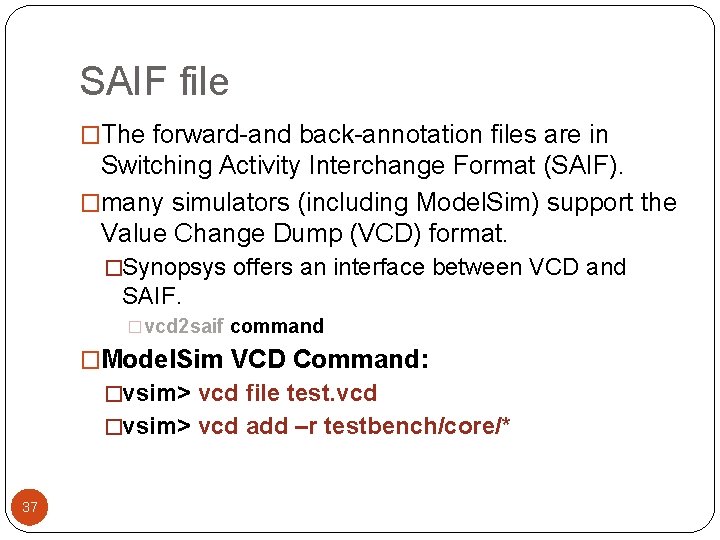
SAIF file �The forward-and back-annotation files are in Switching Activity Interchange Format (SAIF). �many simulators (including Model. Sim) support the Value Change Dump (VCD) format. �Synopsys offers an interface between VCD and SAIF. �vcd 2 saif command �Model. Sim VCD Command: �vsim> vcd file test. vcd �vsim> vcd add –r testbench/core/* 37

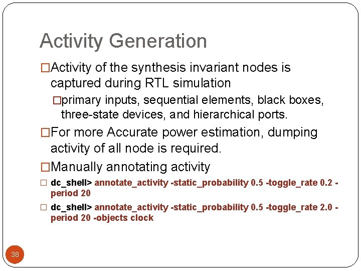
Activity Generation �Activity of the synthesis invariant nodes is captured during RTL simulation �primary inputs, sequential elements, black boxes, three-state devices, and hierarchical ports. �For more Accurate power estimation, dumping activity of all node is required. �Manually annotating activity � dc_shell> annotate_activity -static_probability 0. 5 -toggle_rate 0. 2 - period 20 � dc_shell> annotate_activity -static_probability 0. 5 -toggle_rate 2. 0 - period 20 -objects clock 38

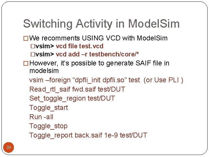
Switching Activity in Model. Sim � We recomments USING VCD with Model. Sim �vsim> vcd file test. vcd �vsim> vcd add –r testbench/core/* � However, it’s possible to generate SAIF file in modelsim vsim –foreign “dpfli_init dpfli. so” test (or Use PLI ) Read_rtl_saif fwd. saif test/DUT Set_toggle_region test/DUT Toggle_start Run -all Toggle_stop Toggle_report back. saif 1 e-9 test/DUT 39

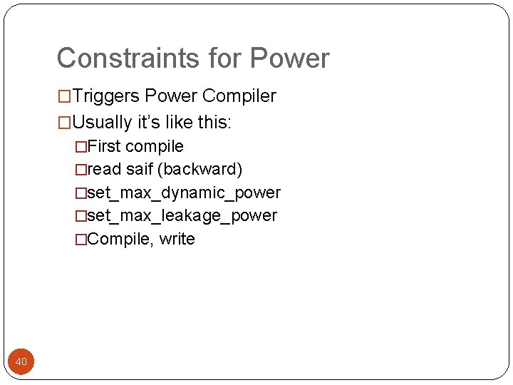
Constraints for Power �Triggers Power Compiler �Usually it’s like this: �First compile �read saif (backward) �set_max_dynamic_power �set_max_leakage_power �Compile, write 40

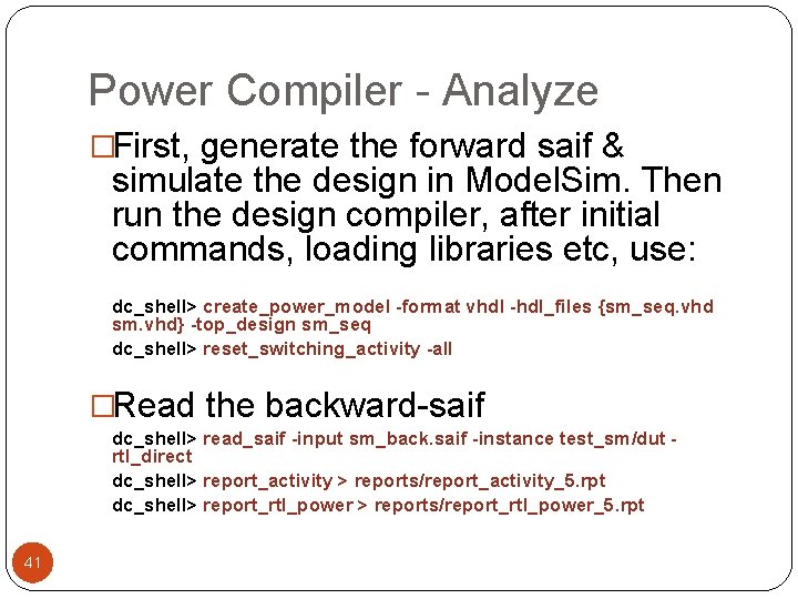
Power Compiler - Analyze �First, generate the forward saif & simulate the design in Model. Sim. Then run the design compiler, after initial commands, loading libraries etc, use: dc_shell> create_power_model -format vhdl -hdl_files {sm_seq. vhd sm. vhd} -top_design sm_seq dc_shell> reset_switching_activity -all �Read the backward-saif dc_shell> read_saif -input sm_back. saif -instance test_sm/dut rtl_direct dc_shell> report_activity > reports/report_activity_5. rpt dc_shell> report_rtl_power > reports/report_rtl_power_5. rpt 41

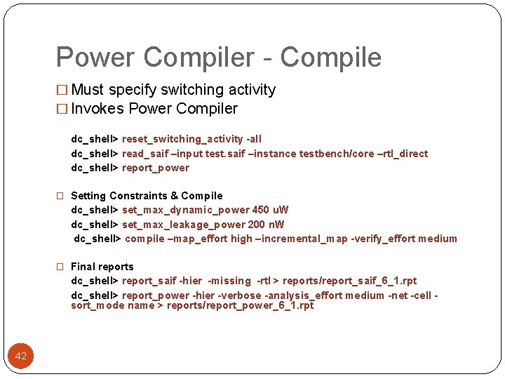
Power Compiler - Compile � Must specify switching activity � Invokes Power Compiler dc_shell> reset_switching_activity -all dc_shell> read_saif –input test. saif –instance testbench/core –rtl_direct dc_shell> report_power � Setting Constraints & Compile dc_shell> set_max_dynamic_power 450 u. W dc_shell> set_max_leakage_power 200 n. W dc_shell> compile –map_effort high –incremental_map -verify_effort medium � Final reports dc_shell> report_saif -hier -missing -rtl > reports/report_saif_6_1. rpt dc_shell> report_power -hier -verbose -analysis_effort medium -net -cell sort_mode name > reports/report_power_6_1. rpt 42

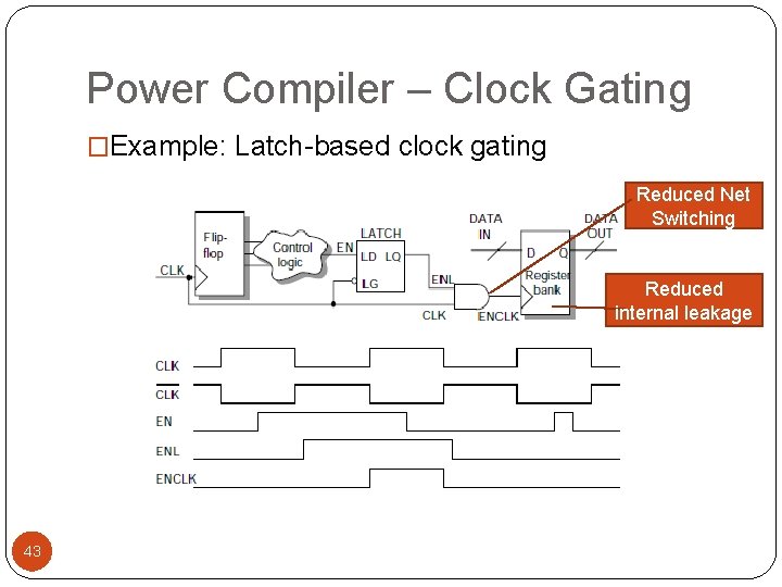
Power Compiler – Clock Gating �Example: Latch-based clock gating Reduced Net Switching Reduced internal leakage 43

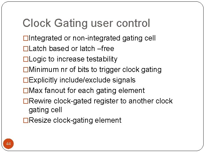
Clock Gating user control �Integrated or non-integrated gating cell �Latch based or latch –free �Logic to increase testability �Minimum nr of bits to trigger clock gating �Explicitly include/exclude signals �Max fanout for each gating element �Rewire clock-gated register to another clock gating cell �Resize clock-gating element 44
![Clock Gating Command setclockgatingstyle sequentialcelllatch none minimumbitwidthvalue setupvalue holdvalue positiveedgelogic gatelist integrated Clock Gating Command set_clock_gating_style [-sequential_celllatch | none] [-minimum_bitwidth_value] [-setup_value] [-hold_value] [-positive_edge_logic{ gate_list | integrated}]](https://slidetodoc.com/presentation_image/56fc45fdb9928e139eac2e2bf0b0be9c/image-45.jpg)
Clock Gating Command set_clock_gating_style [-sequential_celllatch | none] [-minimum_bitwidth_value] [-setup_value] [-hold_value] [-positive_edge_logic{ gate_list | integrated}] [-negative_edge_logic{ gate_list | integrated}] [-control_pointnone | before | after] [-control_signalscan_enable | test_mode] [-observation_pointtrue | false] [-observation_logic_depth_value] [-max_fanout_count] [-no_sharing] 45

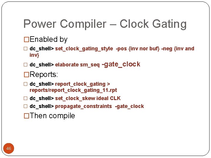
Power Compiler – Clock Gating �Enabled by � dc_shell> set_clock_gating_style -pos {inv nor buf} -neg {inv and inv} � dc_shell> elaborate sm_seq -gate_clock �Reports: � dc_shell> report_clock_gating > reports/report_clock_gating_11. rpt � dc_shell> set_clock_skew ideal CLK � dc_shell> propagate_constraints -gate_clock �Then compile 46

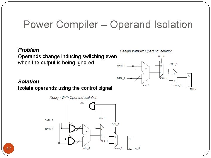
Power Compiler – Operand Isolation Problem Operands change inducing switching even when the output is being ignored Solution Isolate operands using the control signal 47

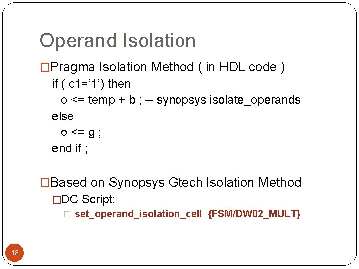
Operand Isolation �Pragma Isolation Method ( in HDL code ) if ( c 1=‘ 1’) then o <= temp + b ; -- synopsys isolate_operands else o <= g ; end if ; �Based on Synopsys Gtech Isolation Method �DC Script: � set_operand_isolation_cell {FSM/DW 02_MULT} 48

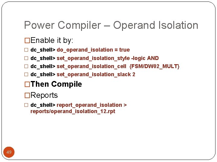
Power Compiler – Operand Isolation �Enable it by: � dc_shell> do_operand_isolation = true � dc_shell> set_operand_isolation_style -logic AND � dc_shell> set_operand_isolation_cell {FSM/DW 02_MULT} � dc_shell> set_operand_isolation_slack 2 �Then Compile �Reports � dc_shell> report_operand_isolation > reports/operand_isolation_12. rpt 49

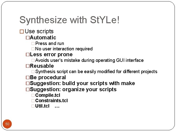
Synthesize with St. YLe! � Use scripts �Automatic � Press and run � No user interaction required �Less error prone � Avoids user’s mistake during operating GUI interface �Reusable � Synthesis script can be easily modified for different projects �Be procedural �Suggestion: build your scripts with make �Suggestion: organize your scripts � Compile. tcl � Constraints. tcl � Util. tcl … 50

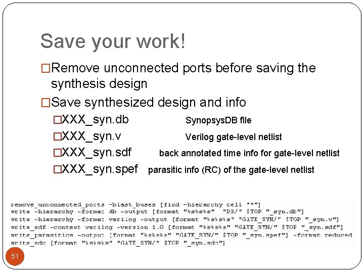
Save your work! �Remove unconnected ports before saving the synthesis design �Save synthesized design and info �XXX_syn. db Synopsys. DB file �XXX_syn. v Verilog gate-level netlist �XXX_syn. sdf back annotated time info for gate-level netlist �XXX_syn. spef parasitic info (RC) of the gate-level netlist 51

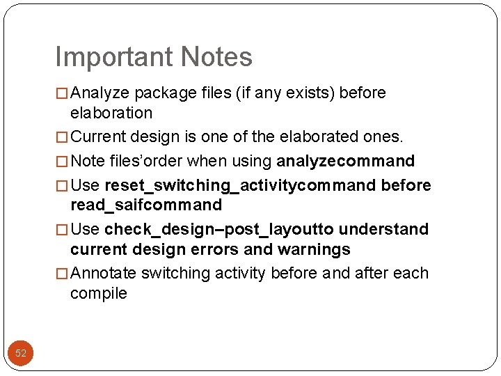
Important Notes � Analyze package files (if any exists) before elaboration � Current design is one of the elaborated ones. � Note files’order when using analyzecommand � Use reset_switching_activitycommand before read_saifcommand � Use check_design–post_layoutto understand current design errors and warnings � Annotate switching activity before and after each compile 52

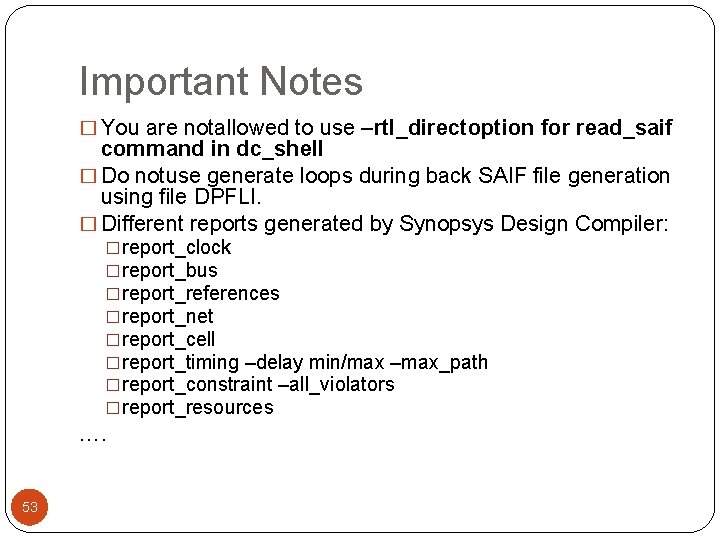
Important Notes � You are notallowed to use –rtl_directoption for read_saif command in dc_shell � Do notuse generate loops during back SAIF file generation using file DPFLI. � Different reports generated by Synopsys Design Compiler: �report_clock �report_bus �report_references �report_net �report_cell �report_timing –delay min/max –max_path �report_constraint –all_violators �report_resources …. 53

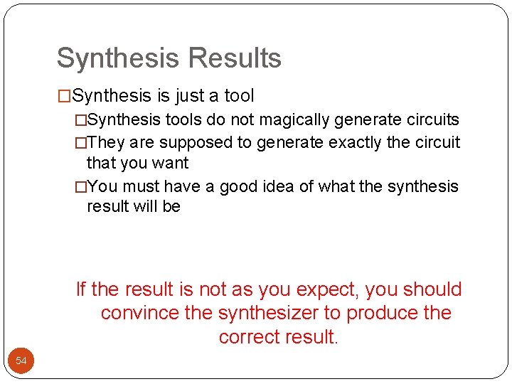
Synthesis Results �Synthesis is just a tool �Synthesis tools do not magically generate circuits �They are supposed to generate exactly the circuit that you want �You must have a good idea of what the synthesis result will be If the result is not as you expect, you should convince the synthesizer to produce the correct result. 54

Back-end design Part I: Placement & Routing 55

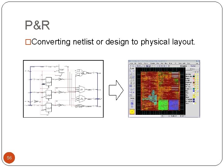
P&R �Converting netlist or design to physical layout. 56

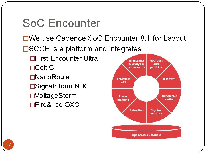
So. C Encounter �We use Cadence So. C Encounter 8. 1 for Layout. �SOCE is a platform and integrates �First Encounter Ultra �Celt. IC �Nano. Route �Signal. Storm NDC �Voltage. Storm �Fire& Ice QXC 57

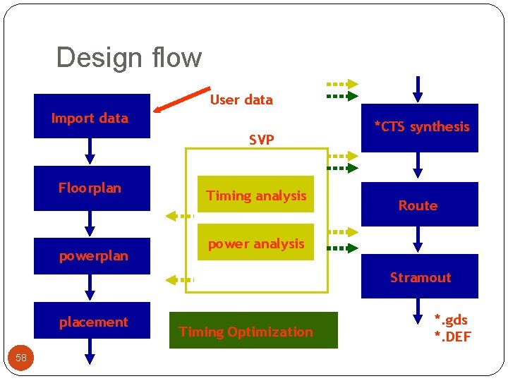
Design flow User data Import data SVP Floorplan powerplan Timing analysis *CTS synthesis Route power analysis Stramout placement 58 Timing Optimization *. gds *. DEF

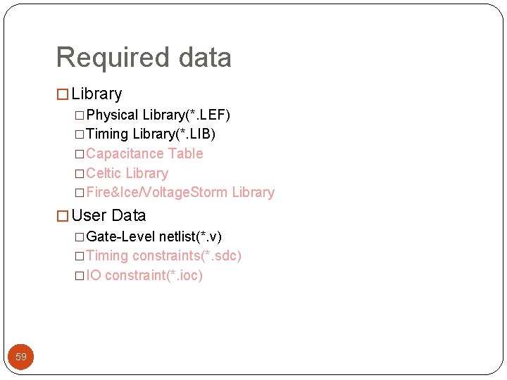
Required data � Library �Physical Library(*. LEF) �Timing Library(*. LIB) �Capacitance Table �Celtic Library �Fire&Ice/Voltage. Storm Library � User Data �Gate-Level netlist(*. v) �Timing constraints(*. sdc) �IO constraint(*. ioc) 59

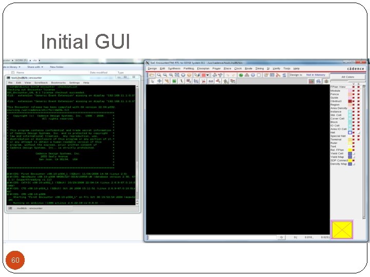
Initial GUI 60

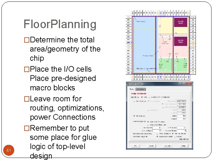
Floor. Planning �Determine the total 61 area/geometry of the chip �Place the I/O cells Place pre-designed macro blocks �Leave room for routing, optimizations, power Connections �Remember to put some place for glue logic of top-level design

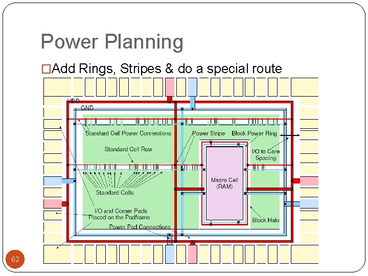
Power Planning �Add Rings, Stripes & do a special route (SROUTE) 62

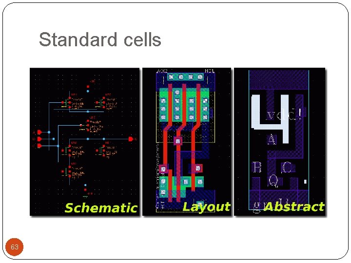
Standard cells 63

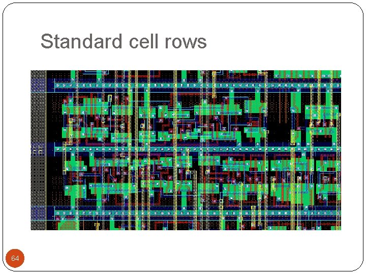
Standard cell rows 64

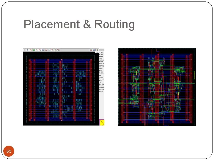
Placement & Routing 65

Placement �NP hard problem �What is the best way of placing the cells within a given area so that: �Critical path is minimum �Long interconnections on the critical path add capacitance �The design is routable �Not all placements can be routed. �The area is minimum �The routing overhead inreases area. 66

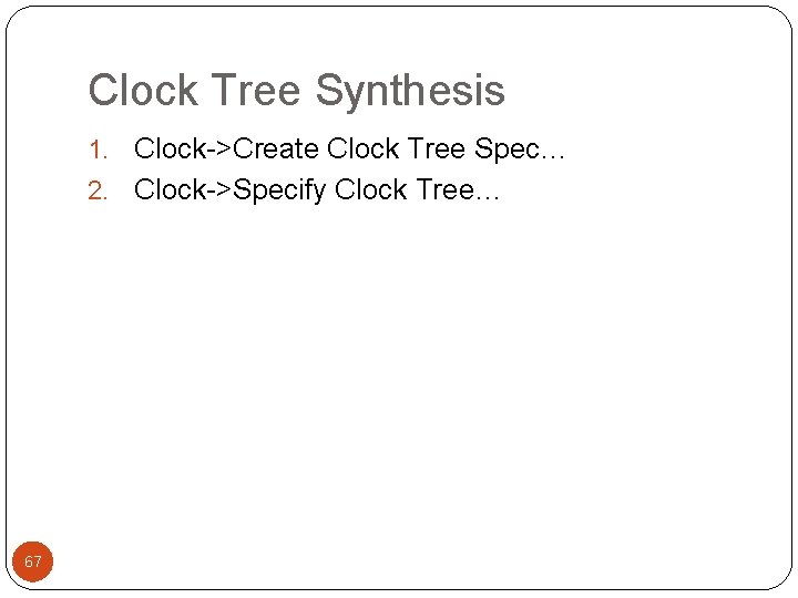
Clock Tree Synthesis Clock->Create Clock Tree Spec… 2. Clock->Specify Clock Tree… 1. 67

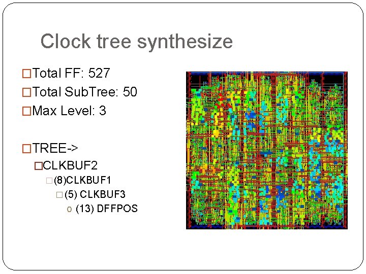
Clock tree synthesize �Total FF: 527 �Total Sub. Tree: 50 �Max Level: 3 �TREE-> �CLKBUF 2 �(8)CLKBUF 1 � (5) CLKBUF 3 o (13) DFFPOS

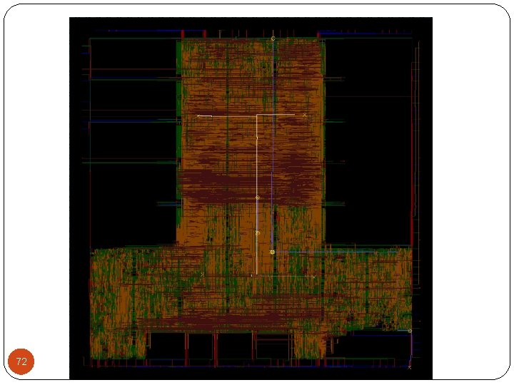
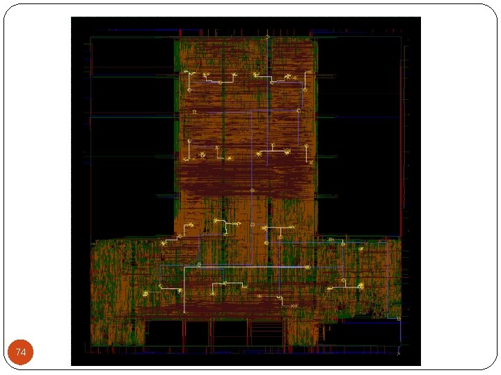
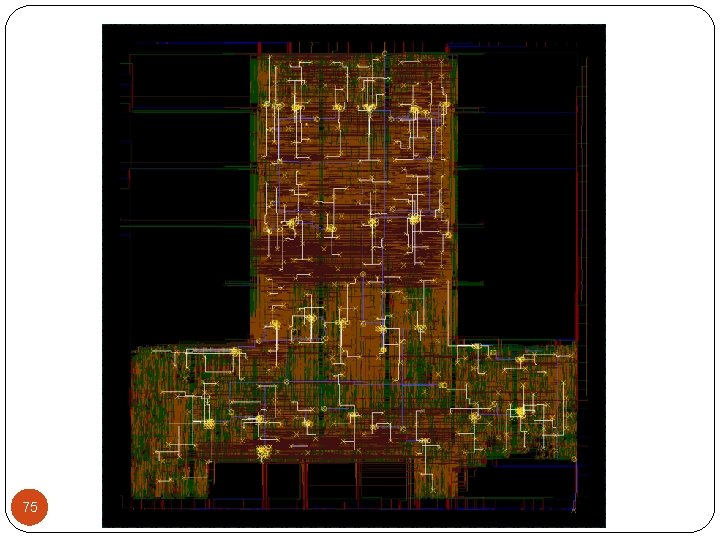
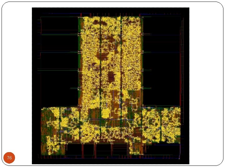
Clock Distribution �Clock is the most critical signal �Standard digital systems rely on the clock signal being present everywhere on the chip at the same time: skew �Clock signal has to be connected to all flip-flops: high fan out �Specialized tools insert multi level buffers (to drive the load) and balance the timing by ensuring the same wirelength for all connection. 69

Clock Distribution example �The following example is a 200 MHz 3 D image renderer with roughly 3 million transistors. The clock distribution has: � 10. 928 flip-flops � 9 level clock tree � 478 buffers in the clock tree � 34 cm total clock wiring �This clock-tree is based on H-Tree 70

71

72

73

74

75

76

Now �Perform Timing Analysis �Perform power analysis �Stream out! 77

Demo Synthesis & P&R 78

Synopsys Prime. Power Estimation 79

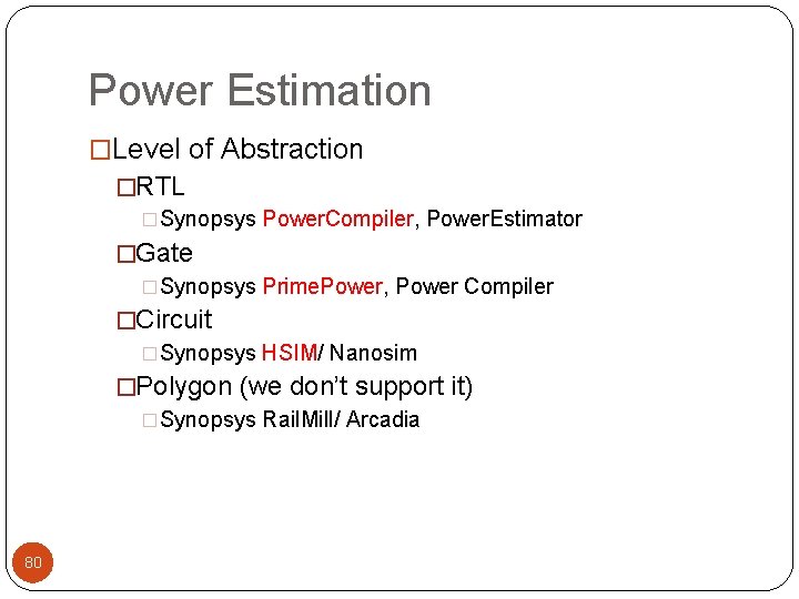
Power Estimation �Level of Abstraction �RTL �Synopsys Power. Compiler, Power. Estimator �Gate �Synopsys Prime. Power, Power Compiler �Circuit �Synopsys HSIM/ Nanosim �Polygon (we don’t support it) �Synopsys Rail. Mill/ Arcadia 80

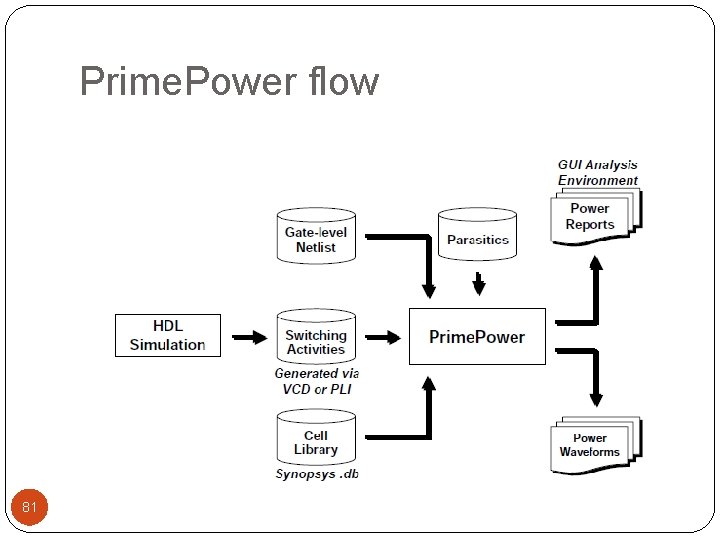
Prime. Power flow 81

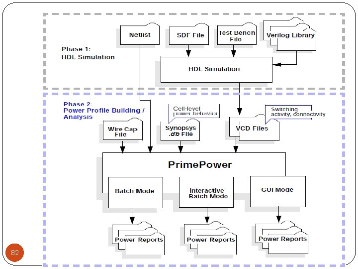
82

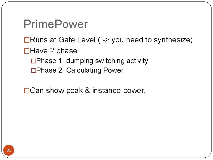
Prime. Power �Runs at Gate Level ( -> you need to synthesize) �Have 2 phase �Phase 1: dumping switching activity �Phase 2: Calculating Power �Can show peak & instance power. 83

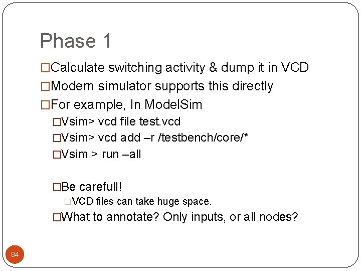
Phase 1 �Calculate switching activity & dump it in VCD �Modern simulator supports this directly �For example, In Model. Sim �Vsim> vcd file test. vcd �Vsim> vcd add –r /testbench/core/* �Vsim > run –all �Be carefull! �VCD files can take huge space. �What to annotate? Only inputs, or all nodes? 84

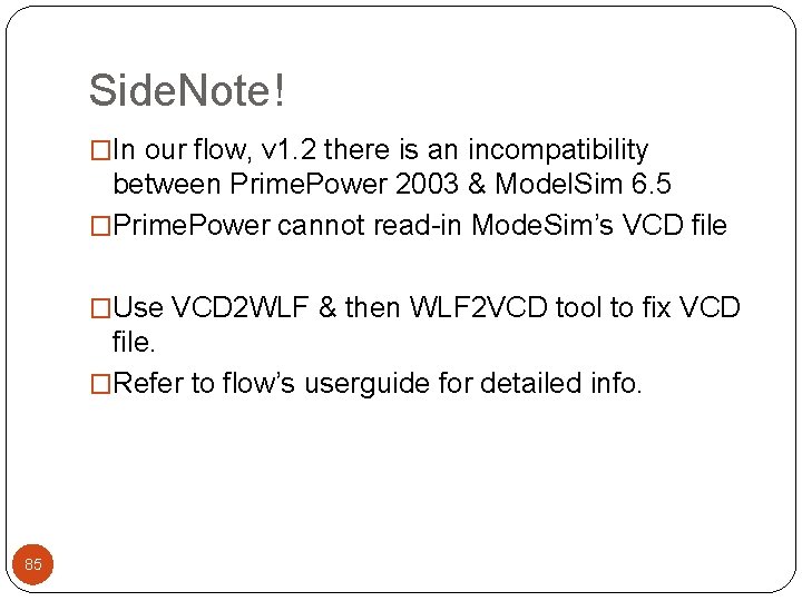
Side. Note! �In our flow, v 1. 2 there is an incompatibility between Prime. Power 2003 & Model. Sim 6. 5 �Prime. Power cannot read-in Mode. Sim’s VCD file �Use VCD 2 WLF & then WLF 2 VCD tool to fix VCD file. �Refer to flow’s userguide for detailed info. 85

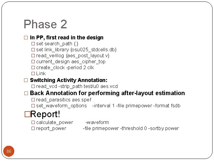
Phase 2 � In PP, first read in the design � set search_path {. } � set link_library {osu 025_stdcells. db} � read_verilog {aes_post_layout. v} � current_design aes_cipher_top � create_clock -period 2 clk � Link � Switching Activity Annotation: � read_vcd -strip_path test/u 0 aes. vcd � Back Annotation for performing after-layout estimation � read_parasitics aes. spef � set_waveform_options -interval 1 -file primepower -format fsdb �Report! � calculate_power � report_power 86 -waveform -file primepower -threshold 0 -sortby power

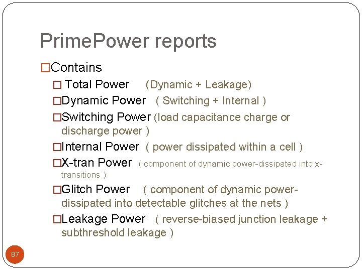
Prime. Power reports �Contains � Total Power (Dynamic + Leakage) �Dynamic Power ( Switching + Internal ) �Switching Power (load capacitance charge or discharge power ) �Internal Power ( power dissipated within a cell ) �X-tran Power ( component of dynamic power-dissipated into xtransitions ) �Glitch Power ( component of dynamic powerdissipated into detectable glitches at the nets ) �Leakage Power ( reverse-biased junction leakage + subthreshold leakage ) 87

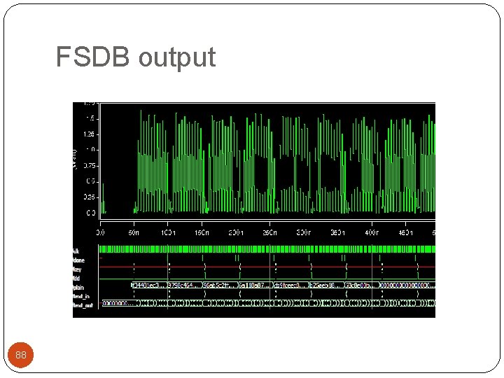
FSDB output 88

Synopsys HSIM Circuit level simulation & co-simulation Post-Layout verification 89

Synopsys HSIM �Hierarchical Storage and Isomorphic Matching �It’s Spice, then �AC analyses �DC analyses �Transient analyses �Monte Carlo analyses �FFT analyses �Sister tools: CRITIC, HANEX �Not supported by synopsys anymore. 90

Synopsys HSIM �First developed by Nassda �Fast SPICE, means it’s event based. � 1, 000 -10, 000 x faster than SPICE with user-selectable accuracy � Hierarchical storage and simulation � Isomorphic matching: duplicate simulated circuit response for isomorphic subcircuits under same conditions. � Does not use simplified model or simulation algorithms. 91 � Similar fast-spice: Synopsys Star-Sim. XT, Synopsys

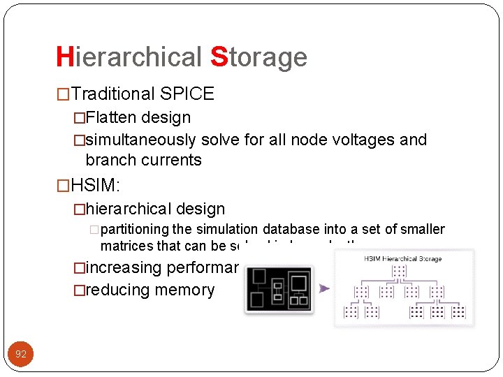
Hierarchical Storage �Traditional SPICE �Flatten design �simultaneously solve for all node voltages and branch currents �HSIM: �hierarchical design �partitioning the simulation database into a set of smaller matrices that can be solved independently �increasing performance �reducing memory 92

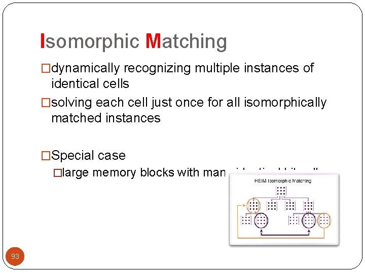
Isomorphic Matching �dynamically recognizing multiple instances of identical cells �solving each cell just once for all isomorphically matched instances �Special case �large memory blocks with many identical bit cells. 93

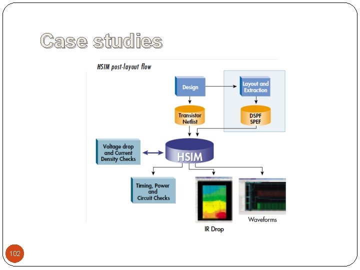
input �HSPICE including triple DES (3 DES) and Verilog- A encryption �Spectre and Eldo-format netlists �VCD and HSPICE vector stimulus �Interpreted and compiled Verilog-A �DPF, SPEF, and DSPF parasitic formats 94

output �ASCII. out and raw formats �WSF, PSF-float �WDF �FSDB �UTF �. measure, built-in timing and power checks 95

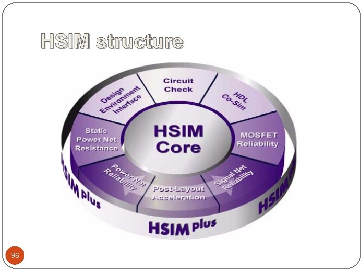
HSIM structure 96

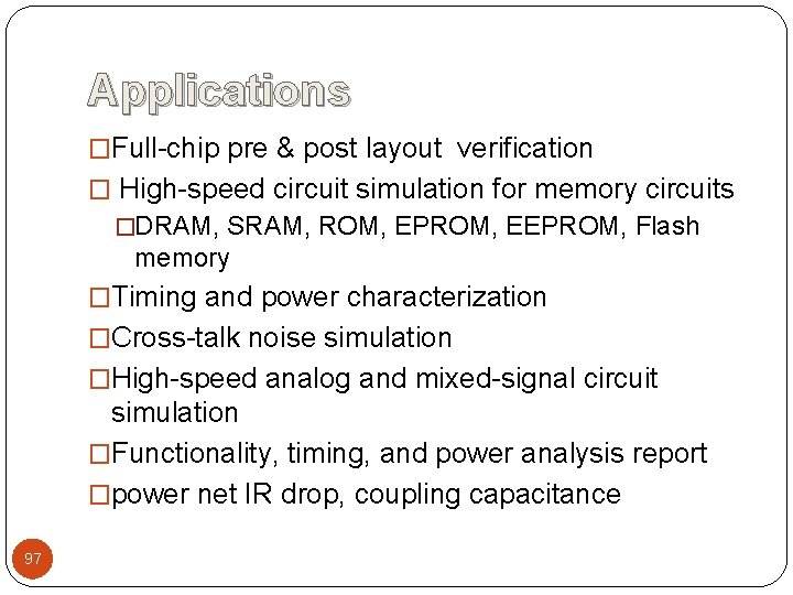
Applications �Full-chip pre & post layout verification � High-speed circuit simulation for memory circuits �DRAM, SRAM, ROM, EPROM, EEPROM, Flash memory �Timing and power characterization �Cross-talk noise simulation �High-speed analog and mixed-signal circuit simulation �Functionality, timing, and power analysis report �power net IR drop, coupling capacitance 97

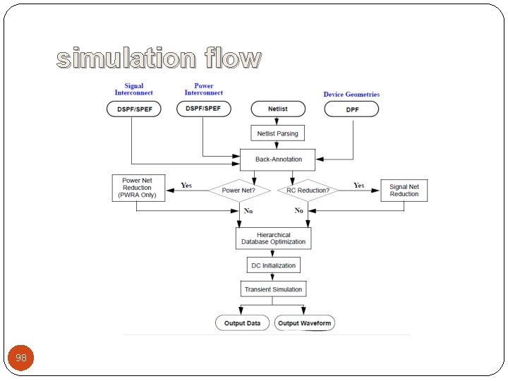
simulation flow 98

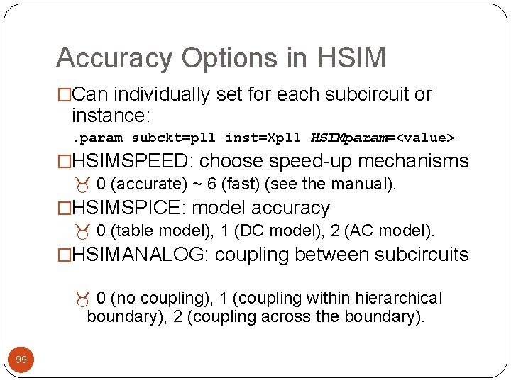
Accuracy Options in HSIM �Can individually set for each subcircuit or instance: . param subckt=pll inst=Xpll HSIMparam=<value> �HSIMSPEED: choose speed-up mechanisms 0 (accurate) ~ 6 (fast) (see the manual). �HSIMSPICE: model accuracy 0 (table model), 1 (DC model), 2 (AC model). �HSIMANALOG: coupling between subcircuits 0 (no coupling), 1 (coupling within hierarchical boundary), 2 (coupling across the boundary). 99

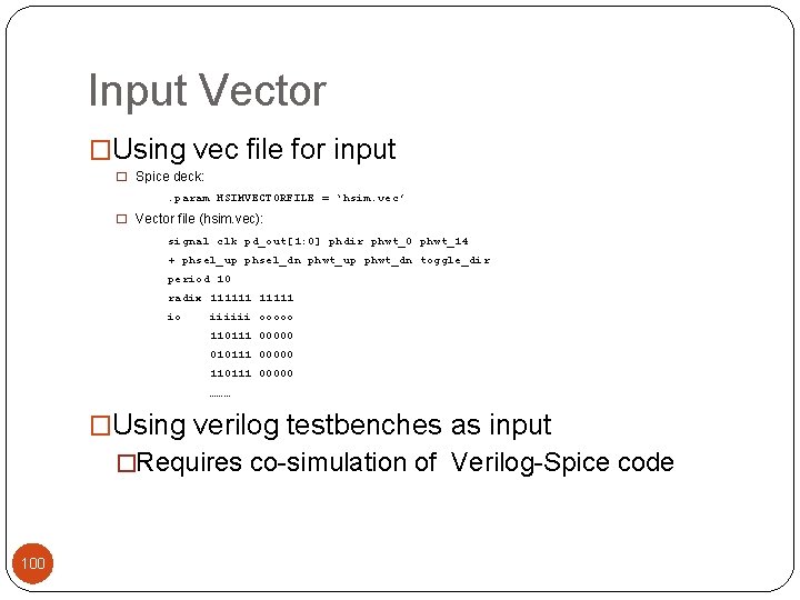
Input Vector �Using vec file for input � Spice deck: . param HSIMVECTORFILE = ‘hsim. vec’ � Vector file (hsim. vec): signal clk pd_out[1: 0] phdir phwt_0 phwt_14 + phsel_up phsel_dn phwt_up phwt_dn toggle_dir period 10 radix 111111 io iiiiii ooooo 110111 00000 010111 00000 110111 00000 ……… �Using verilog testbenches as input �Requires co-simulation of Verilog-Spice code 100

Case studies �Post-layout back-annotation �Mixed-Signal Simulation �Verilog-A support �V 2 S �Timing & Power Analysis 101

Case studies 102

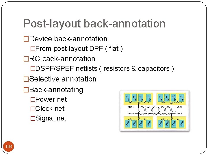
Post-layout back-annotation �Device back-annotation �From post-layout DPF ( flat ) �RC back-annotation �DSPF/SPEF netlists ( resistors & capacitors ) �Selective annotation �Back-annotating �Power net �Clock net �Signal net 103

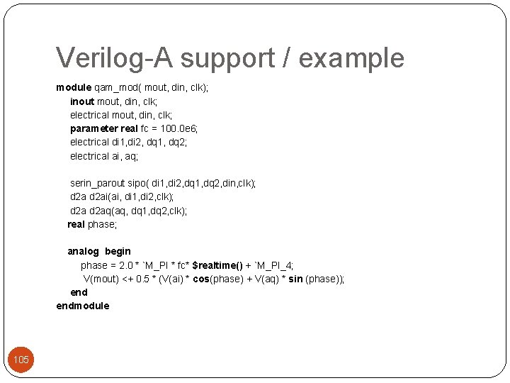
Verilog-A support �Analog Enhancement to Verilog. �Good for describing a behavioral model of devices. �I’ve the models of following devices: �BSIM 3 v 3, BSIM 4, EKV, HISIM, Level 3, BJT, MEXTRAN, VBIC, TFT, fbh_hbt, Hicum, JFET 104

Verilog-A support / example module qam_mod( mout, din, clk); inout mout, din, clk; electrical mout, din, clk; parameter real fc = 100. 0 e 6; electrical di 1, di 2, dq 1, dq 2; electrical ai, aq; serin_parout sipo( di 1, di 2, dq 1, dq 2, din, clk); d 2 ai(ai, di 1, di 2, clk); d 2 aq(aq, dq 1, dq 2, clk); real phase; analog begin phase = 2. 0 * `M_PI * fc* $realtime() + `M_PI_4; V(mout) <+ 0. 5 * (V(ai) * cos(phase) + V(aq) * sin (phase)); endmodule 105

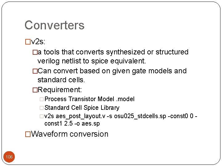
Converters �v 2 s: �a tools that converts synthesized or structured verilog netlist to spice equivalent. �Can convert based on given gate models and standard cells. �Requirement: �Process Transistor Model. model �Standard Cell Spice Library �v 2 s aes_post_layout. v -s osu 025_stdcells. sp -const 0 0 - const 1 2. 5 -o aes. sp �Waveform conversion 106

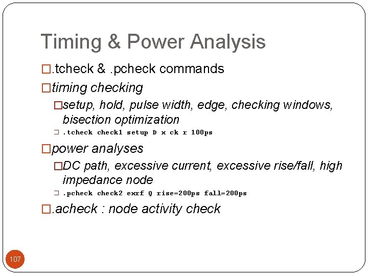
Timing & Power Analysis �. tcheck &. pcheck commands �timing checking �setup, hold, pulse width, edge, checking windows, bisection optimization �. tcheck 1 setup D x ck r 100 ps �power analyses �DC path, excessive current, excessive rise/fall, high impedance node �. pcheck 2 exrf Q rise=200 ps fall=200 ps �. acheck : node activity check 107

Other features not covered here �Post-Layout Acceleration Option (PLX) �Power Net Reliability Analysis Option (PWRA) �Static Power Net Resistance Calculation Option (SPRES) �Signal Net Reliability Analysis Option (SIGRA) �MOS Reliability Option (MOSRA) 108

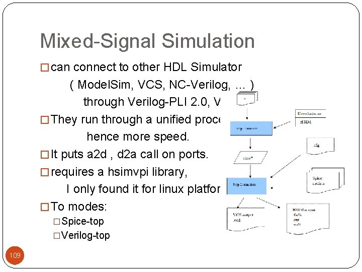
Mixed-Signal Simulation � can connect to other HDL Simulator ( Model. Sim, VCS, NC-Verilog, … ) through Verilog-PLI 2. 0, VPI � They run through a unified process, hence more speed. � It puts a 2 d , d 2 a call on ports. � requires a hsimvpi library, I only found it for linux platform. � To modes: �Spice-top �Verilog-top 109

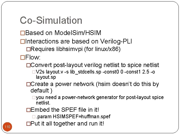
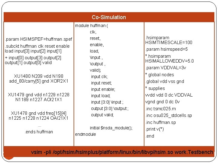
Co-Simulation �Based on Model. Sim/HSIM �Interactions are based on Verilog-PLI �Requires libhsimvpi (for linux/x 86) �Flow: �Convert post-layout verilog netlist to spice netlist �V 2 s layout. v -s lib_stdcells. sp -const 0 0 -const 1 2. 5 -o layout. sp �Create a power network (hsim doesn’t do this by default ) �you need a power-network generator for post-layout spice netlist. 110 �Embed the SPEF file in it! �. param HSIMSPEF=huffman. spef �Put it all together and run it!

Co-Simulation module huffman ( clk, . param HSIMSPEF=huffman. spef. subckt huffman clk reset enable load input[3] input[2] input[1] + input[0] output[3] output[2] output[1] output[0] valid XU 1480 N 209 vdd N 198 add_80/carry[5] gnd XOR 2 X 1 XU 1479 gnd vdd n 1229 n 1228 N 1189 n 1227 AOI 21 X 1 XU 1478 gnd vdd freq[15][4] n 1225 n 1228 n 1224 OAI 21 X 1. . ends huffman 111 reset, enable, load, input , output , valid); input clk; input reset; input enable; input load; input [3: 0] input ; output [3: 0] output ; output valid; initial $nsda_module(); endmodule . hsimparam HSIMTIMESCALE=100. param hsimspeed=5 *. hsimparam HSIMALLOWEDDV=5. 0. param VDDVAL=3 v * global nodes. global vdd vss gnd * supplies vvdd 0 dc VDDVAL vgnd 0 dc 0 v. inc tsmc 025. m. inc osu 025_stdcells. sp. inc huffman. sp. print v(*). end vsim -pli /opt/hsimplus/platform/linux/bin/libvpihsim. so work. Testbench

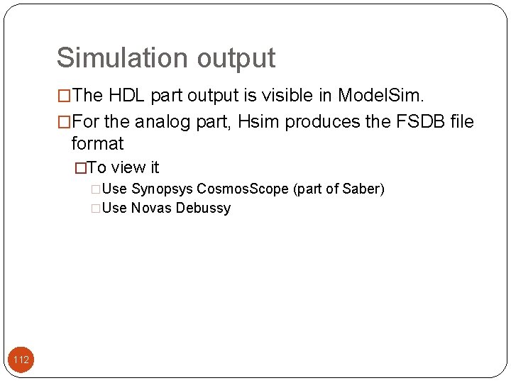
Simulation output �The HDL part output is visible in Model. Sim. �For the analog part, Hsim produces the FSDB file format �To view it �Use Synopsys Cosmos. Scope (part of Saber) �Use Novas Debussy 112

Sample HSIM flow 113

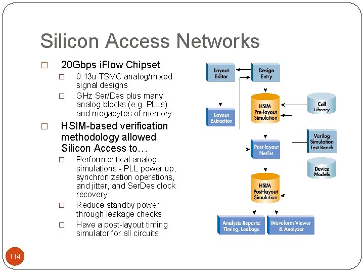
Silicon Access Networks � 20 Gbps i. Flow Chipset � � � HSIM-based verification methodology allowed Silicon Access to… � � � 114 0. 13 u TSMC analog/mixed signal designs GHz Ser/Des plus many analog blocks (e. g. PLLs) and megabytes of memory Perform critical analog simulations - PLL power up, synchronization operations, and jitter, and Ser. Des clock recovery Reduce standby power through leakage checks Have a post-layout timing simulator for all circuits

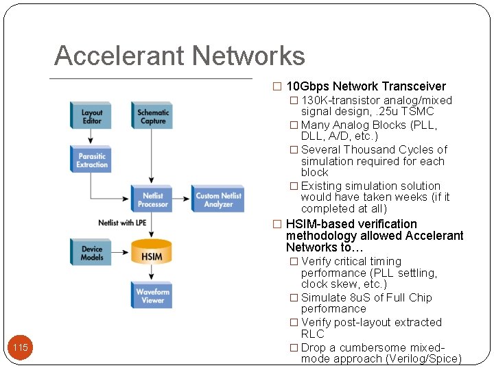
Accelerant Networks � 10 Gbps Network Transceiver � 130 K-transistor analog/mixed signal design, . 25 u TSMC � Many Analog Blocks (PLL, DLL, A/D, etc. ) � Several Thousand Cycles of simulation required for each block � Existing simulation solution would have taken weeks (if it completed at all) � HSIM-based verification methodology allowed Accelerant Networks to… � Verify critical timing 115 performance (PLL settling, clock skew, etc. ) � Simulate 8 u. S of Full Chip performance � Verify post-layout extracted RLC � Drop a cumbersome mixedmode approach (Verilog/Spice)
![Sharif Dependable System Lab DSL HSIM were used as part of fault injection flow Sharif Dependable System Lab [DSL] �HSIM were used as part of fault injection flow](https://slidetodoc.com/presentation_image/56fc45fdb9928e139eac2e2bf0b0be9c/image-116.jpg)
Sharif Dependable System Lab [DSL] �HSIM were used as part of fault injection flow to evaluate reliability of a processor design �Mixed-signal simulation at three-level of abstraction �Fault is injected in Verilog-A module, attached to Spice netlist using external circuit (X). 116
![Sharif Dependable System Lab DSL 117 Sharif Dependable System Lab [DSL] 117](https://slidetodoc.com/presentation_image/56fc45fdb9928e139eac2e2bf0b0be9c/image-117.jpg)
Sharif Dependable System Lab [DSL] 117
![Sharif Dependable System Lab DSL With HSIM We get an accurate simulation of fault Sharif Dependable System Lab [DSL] �With HSIM �We get an accurate simulation of fault,](https://slidetodoc.com/presentation_image/56fc45fdb9928e139eac2e2bf0b0be9c/image-118.jpg)
Sharif Dependable System Lab [DSL] �With HSIM �We get an accurate simulation of fault, near the fault site. �Fault injection on memory modules (SRAM, DRAM, …) is very fast. �The rest of the design is simulated in Model. Sim � Speed penalty for fault injection is very low. �Fault Injection on Analog modules or modules that doesn’t have HDL description. ( robust SRAM, DRAMs, delayed Latches, PLLs, etc. ) �Behavioral fault injection in Verilog-A �We can explore various fault models. �Currently we support : SET/SEU, EMI, PSD, Temp. Variation. 118

Tool demonstration 119

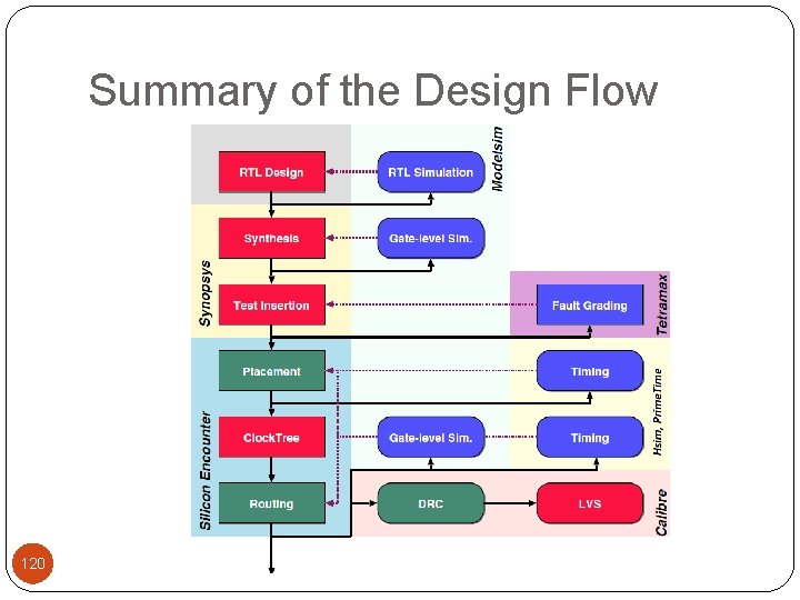
Summary of the Design Flow 120

High-Speed Digital Design checklist 121

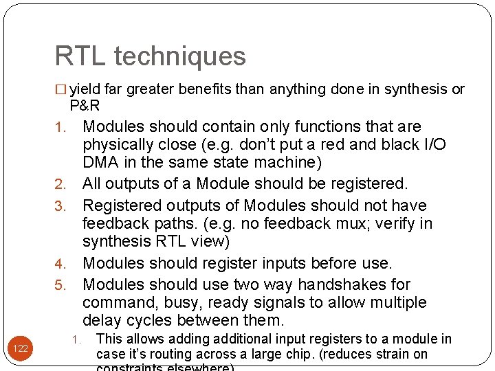
RTL techniques � yield far greater benefits than anything done in synthesis or P&R Modules should contain only functions that are physically close (e. g. don’t put a red and black I/O DMA in the same state machine) All outputs of a Module should be registered. Registered outputs of Modules should not have feedback paths. (e. g. no feedback mux; verify in synthesis RTL view) Modules should register inputs before use. Modules should use two way handshakes for command, busy, ready signals to allow multiple delay cycles between them. 1. 2. 3. 4. 5. 122 1. This allows adding additional input registers to a module in case it’s routing across a large chip. (reduces strain on

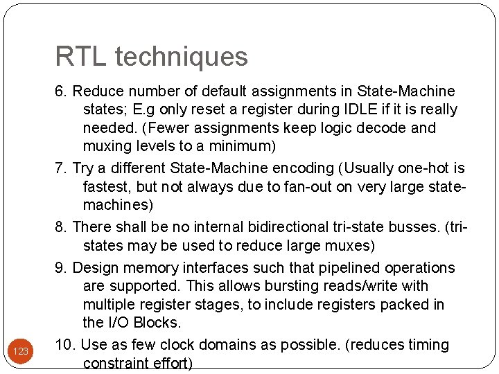
RTL techniques 123 6. Reduce number of default assignments in State-Machine states; E. g only reset a register during IDLE if it is really needed. (Fewer assignments keep logic decode and muxing levels to a minimum) 7. Try a different State-Machine encoding (Usually one-hot is fastest, but not always due to fan-out on very large statemachines) 8. There shall be no internal bidirectional tri-state busses. (tristates may be used to reduce large muxes) 9. Design memory interfaces such that pipelined operations are supported. This allows bursting reads/write with multiple register stages, to include registers packed in the I/O Blocks. 10. Use as few clock domains as possible. (reduces timing constraint effort)

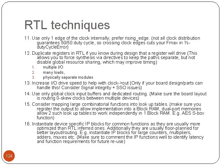
RTL techniques 11. Use only 1 edge of the clock internally; prefer rising_edge. (not all clock distribution guarantees 50/50 duty cycle, so crossing clock edges cuts your Fmax in ½ duty. Cycle. Error) 12. Duplicate registers in RTL if you know during design that a register will drive (This allows you to force synthesis via directives to keep the paths separate, but not disable global resource sharing, which may improve timing) 1. 2. 3. multiple I/O many loads, physically separate modules 13. Increase I/O drive speed to help with clock->out (Only if your board design/parts can handle this! Consider Signal integrity + SSO issues) 14. Use only global clock input buffers and dedicated routing. (Make sure the board layout is routing 0 -skew clocks between multiple devices) 15. Consider mapping large combinatorial functions into look up tables. (make sure you register the output to allow implementation into a Block RAM; dual-port memories allow 2 such look up tables to work independently in 1 Block RAM. E. g. AES S-box function) 16. Instantiate device specific IP blocks for common functions as they are usually more optimized than RTL inferred ones. Additionally they are usually floor-planned for better layout/routing. E. g. instantiate IP blocks for large counters, multipliers, adders, muxes etc. (Make sure to comment the IP functions well to identify latency and function requirements for future re-use) 124

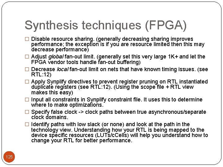
Synthesis techniques (FPGA) � Disable resource sharing. (generally decreasing sharing improves � � � 125 performance; the exception is if you are resource limited then this may decrease performance) Adjust global fan-out limit. (generally set this very large 1 K+ and let the FPGA vendor tools handle fan-out buffering) Decrease local fan-out limit on nets that have known timing issues. (see RTL: 12) Apply Synplify directives to prevent register pruning on RTL instantiated duplicate registers (see RTL: 12). (Using the scope file + RTL view makes this easy) Input all constraints in Synplify constraint file. It uses this to determine where to make optimizations. Specify false clock -> clock paths between true asynchronous/separate clock domains. Identify paths with low slack (or none) and look at the path in the technology view. Understanding how your RTL is being mapped to the device specific resources (LUTs/c. Cells) will help you understand how to change your RTL for better performance.

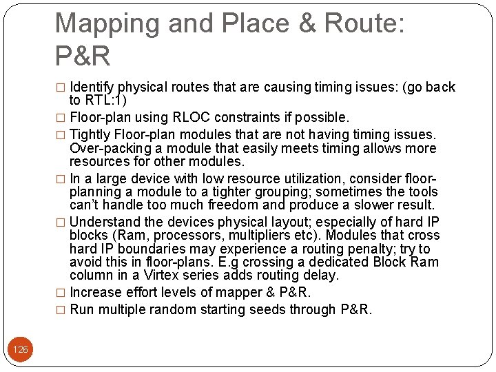
Mapping and Place & Route: P&R � Identify physical routes that are causing timing issues: (go back to RTL: 1) � Floor-plan using RLOC constraints if possible. � Tightly Floor-plan modules that are not having timing issues. Over-packing a module that easily meets timing allows more resources for other modules. � In a large device with low resource utilization, consider floorplanning a module to a tighter grouping; sometimes the tools can’t handle too much freedom and produce a slower result. � Understand the devices physical layout; especially of hard IP blocks (Ram, processors, multipliers etc). Modules that cross hard IP boundaries may experience a routing penalty; try to avoid this in floor-plans. E. g crossing a dedicated Block Ram column in a Virtex series adds routing delay. � Increase effort levels of mapper & P&R. � Run multiple random starting seeds through P&R. 126

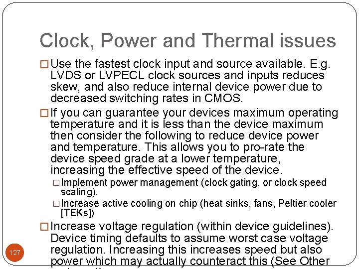
Clock, Power and Thermal issues � Use the fastest clock input and source available. E. g. LVDS or LVPECL clock sources and inputs reduces skew, and also reduce internal device power due to decreased switching rates in CMOS. � If you can guarantee your devices maximum operating temperature and it is less than the device maximum then consider the following to reduce device power and temperature. This allows you to pro-rate the device speed grade at a lower temperature, increasing the effective speed of the device. �Implement power management (clock gating, or clock speed scaling). �Increase active cooling on chip (heat sinks, fans, Peltier cooler [TEKs]) � Increase voltage regulation (within device guidelines). 127 Device timing defaults to assume worst case voltage regulation. Increasing this increases speed but also power which may actually counteract this (See Other

Thank you! Questions? 128