Serial versus Parallel Data Transfers OUTLINE 12212021 l
- Slides: 19

Serial versus Parallel Data Transfers OUTLINE: 12/21/2021 l Shift Registers l Converting data from Serial Parallel Costas Foudas, Imperial College, Rm: 508, x 47590 1

Shift Registers convert numbers expressed in terms of several bits (many signal lines) into a stream of 0, 1 and a Clock. Advantage: A convenient way to reduce the number of Electrical signal lines by factors of 8, 16, 32, 64. Disadvantage: For the same transfer rate the electronics must be faster by factors of 8, 16, 32, 64. 12/21/2021 Costas Foudas, Imperial College, Rm: 508, x 47590 2

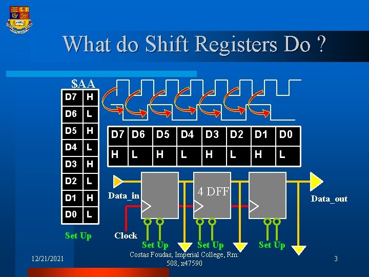
What do Shift Registers Do ? $AA D 7 H D 6 L D 5 H D 4 L D 3 H D 2 L D 1 H D 0 L Set Up 12/21/2021 D 7 D 6 D 5 D 4 D 3 D 2 D 1 D 0 H H L H L L 4 DFF Data_in Clock Set Up Costas Foudas, Imperial College, Rm: 508, x 47590 Data_out Set Up 3

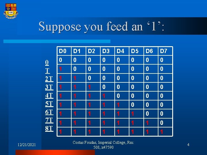
Suppose you feed an ‘ 1’: 0 T 2 T 3 T 4 T 5 T 6 T 7 T 8 T 12/21/2021 D 0 D 1 D 2 D 3 D 4 D 5 D 6 D 7 0 0 0 0 1 1 0 0 0 1 1 0 0 1 1 1 0 0 0 1 1 1 1 0 1 1 1 1 Costas Foudas, Imperial College, Rm: 508, x 47590 4

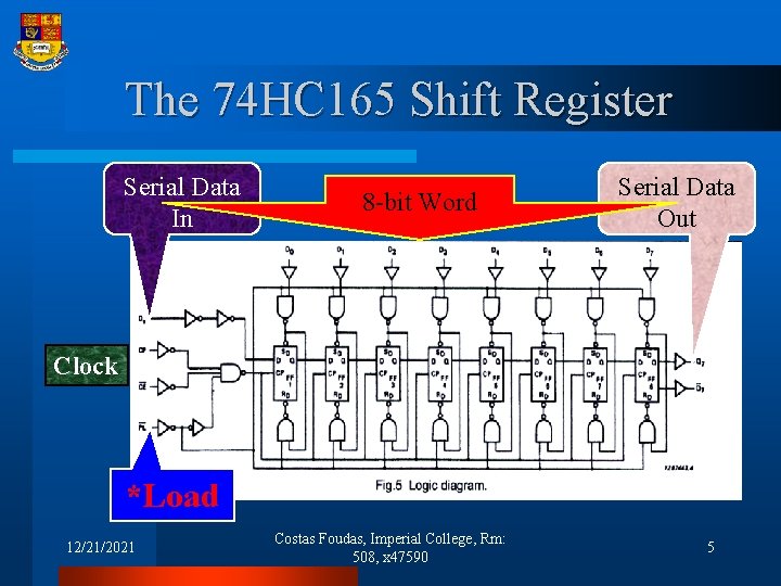
The 74 HC 165 Shift Register Serial Data In 8 -bit Word Serial Data Out Clock *Load 12/21/2021 Costas Foudas, Imperial College, Rm: 508, x 47590 5

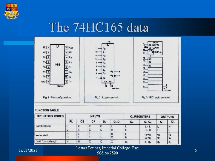
The 74 HC 165 data 12/21/2021 Costas Foudas, Imperial College, Rm: 508, x 47590 6

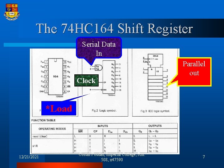
The 74 HC 164 Shift Register Serial Data In Clock Parallel out *Load 12/21/2021 Costas Foudas, Imperial College, Rm: 508, x 47590 7

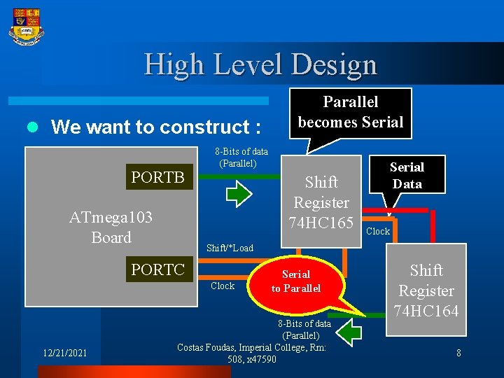
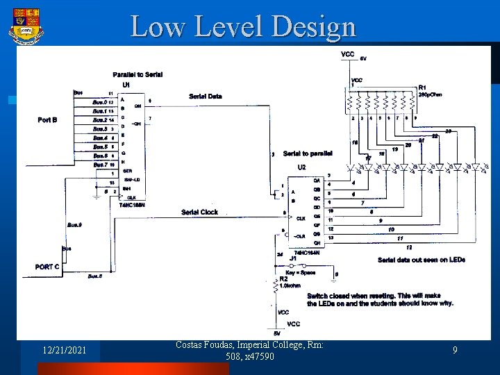
High Level Design l We want to construct : PORTB ATmega 103 Board 8 -Bits of data (Parallel) Shift Register 74 HC 165 Serial Data Clock Shift/*Load PORTC Clock 12/21/2021 Parallel becomes Serial to Parallel 8 -Bits of data (Parallel) Costas Foudas, Imperial College, Rm: 508, x 47590 Shift Register 74 HC 164 8

Low Level Design 12/21/2021 Costas Foudas, Imperial College, Rm: 508, x 47590 9

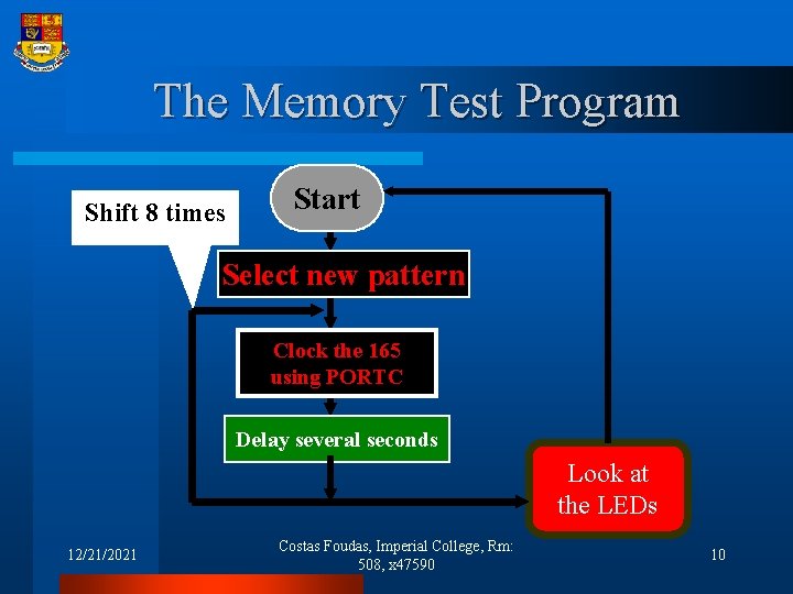
The Memory Test Program Shift 8 times Start Select new pattern Clock the 165 using PORTC Delay several seconds Look at the LEDs 12/21/2021 Costas Foudas, Imperial College, Rm: 508, x 47590 10

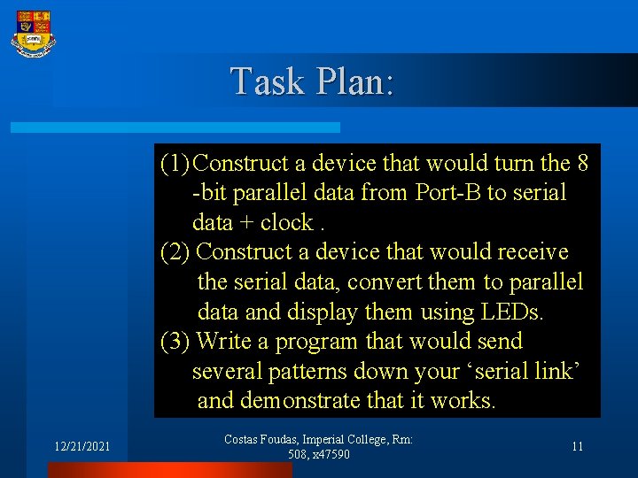
Task Plan: (1) Construct a device that would turn the 8 -bit parallel data from Port-B to serial data + clock. (2) Construct a device that would receive the serial data, convert them to parallel data and display them using LEDs. (3) Write a program that would send several patterns down your ‘serial link’ and demonstrate that it works. 12/21/2021 Costas Foudas, Imperial College, Rm: 508, x 47590 11

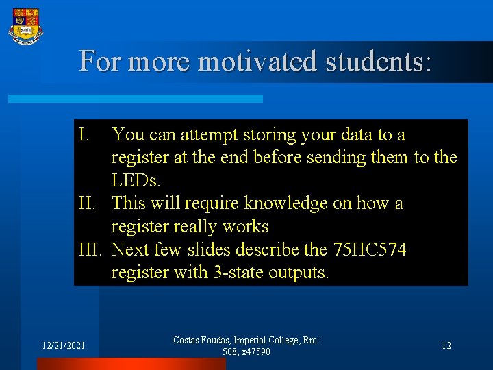
For more motivated students: I. You can attempt storing your data to a register at the end before sending them to the LEDs. II. This will require knowledge on how a register really works III. Next few slides describe the 75 HC 574 register with 3 -state outputs. 12/21/2021 Costas Foudas, Imperial College, Rm: 508, x 47590 12

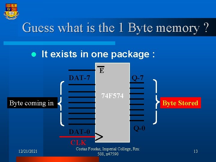
Guess what is the 1 Byte memory ? l It exists in one package : Byte coming in 12/21/2021 DAT-7 E Q-7 74 F 574 DAT-0 CLK Q-0 Costas Foudas, Imperial College, Rm: 508, x 47590 Byte Stored 13

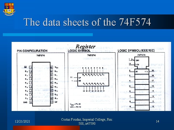
The data sheets of the 74 F 574 Register 12/21/2021 Costas Foudas, Imperial College, Rm: 508, x 47590 14

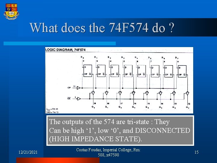
What does the 74 F 574 do ? The outputs of the 574 are tri-state : They Can be high ‘ 1’, low ‘ 0’, and DISCONNECTED (HIGH IMPEDANCE STATE). 12/21/2021 Costas Foudas, Imperial College, Rm: 508, x 47590 15

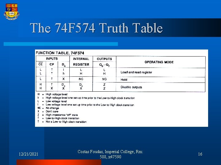
The 74 F 574 Truth Table 12/21/2021 Costas Foudas, Imperial College, Rm: 508, x 47590 16

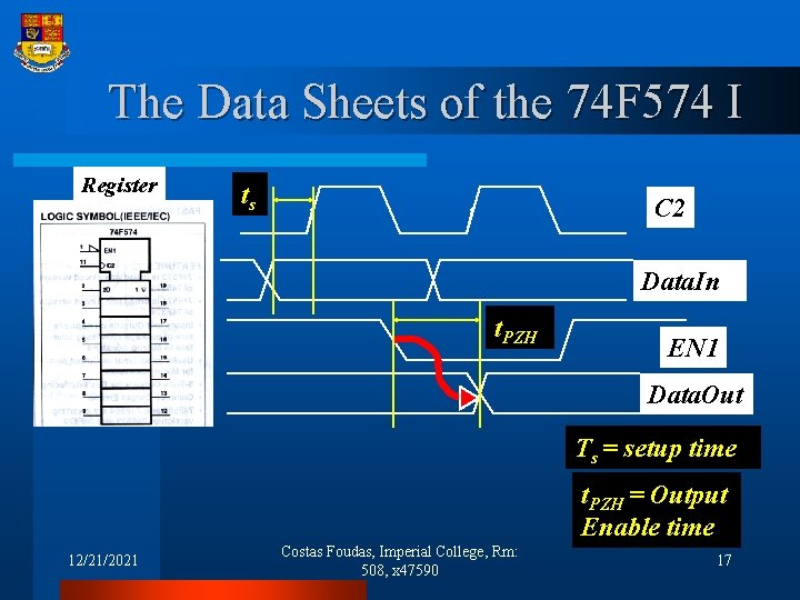
The Data Sheets of the 74 F 574 I Register ts C 2 Data. In t. PZH EN 1 Data. Out Ts = setup time t. PZH = Output Enable time 12/21/2021 Costas Foudas, Imperial College, Rm: 508, x 47590 17

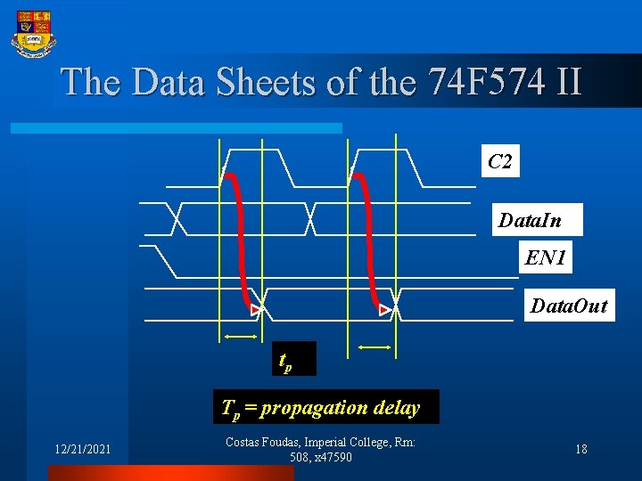
The Data Sheets of the 74 F 574 II C 2 Data. In EN 1 Data. Out tp Tp = propagation delay 12/21/2021 Costas Foudas, Imperial College, Rm: 508, x 47590 18

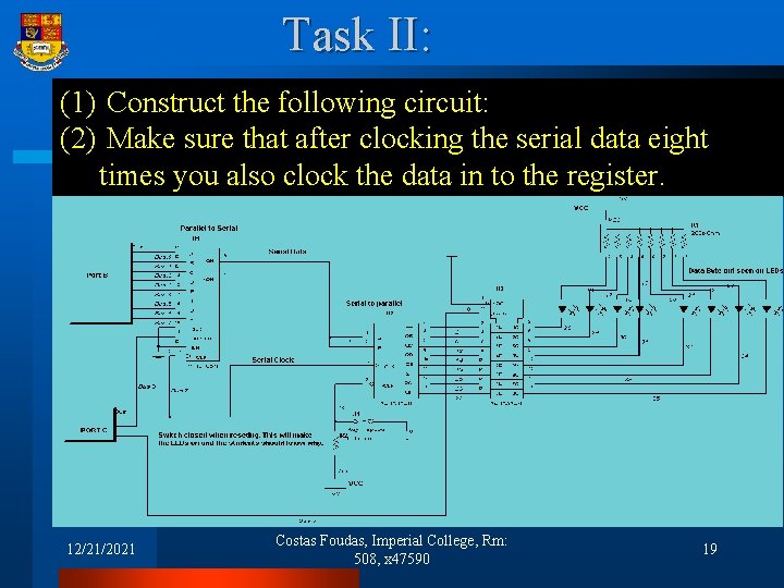
Task II: (1) Construct the following circuit: (2) Make sure that after clocking the serial data eight times you also clock the data in to the register. 12/21/2021 Costas Foudas, Imperial College, Rm: 508, x 47590 19