Sequential Logic An Overview Digital Electronics Sequential Logic

- Slides: 17

Sequential Logic An Overview Digital Electronics

Sequential Logic This presentation will • Introduce the basics of combinational and sequential logic. • Present the logic symbol and function table for the “D” flip-flop. • Review the design for a simple sequential logic circuit. 2

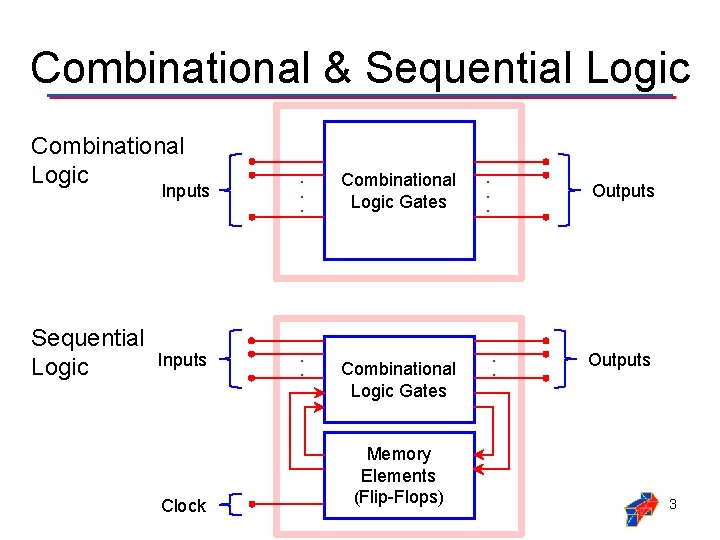
Combinational & Sequential Logic Combinational Logic Sequential Logic Inputs . . Clock Combinational Logic Gates Memory Elements (Flip-Flops) . . . Outputs 3

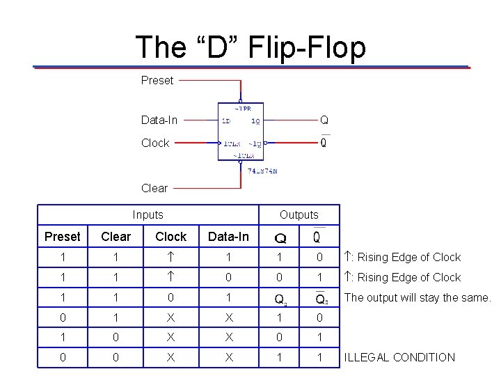
The “D” Flip-Flop Preset Q Data-In Clock Clear Inputs Outputs Preset Clear Clock Data-In 1 1 0 : Rising Edge of Clock 1 1 0 0 1 : Rising Edge of Clock 1 1 0 1 X X 1 0 X X 0 1 0 0 X X 1 1 The output will stay the same. ILLEGAL CONDITION 4

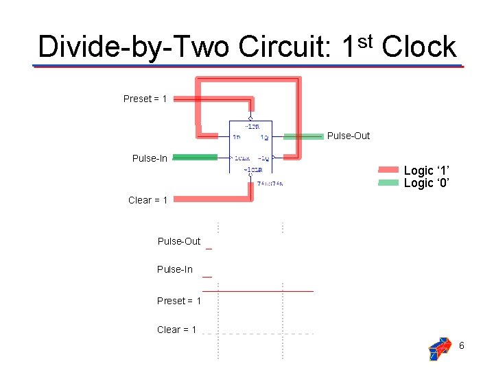
Sequential Logic • The “D” flip-flop is just one of several types of flip -flops that can be used to implement sequential logic designs. • This presentation will look at the Divide-by-Two circuit. • This sample flip-flop application can be implemented with “D” flip-flops. Unit 3 of this course will spend a significant amount of time exploring other flip-flops and their applications. • The purpose of this introduction is to provide a basis of understanding for the sequential logic subsection of the Board Game Counter design. 5

Divide-by-Two Circuit: 1 st Clock Preset = 1 Pulse-Out Pulse-In Logic ‘ 1’ Logic ‘ 0’ Clear = 1 Pulse-Out Pulse-In Preset = 1 Clear = 1 6

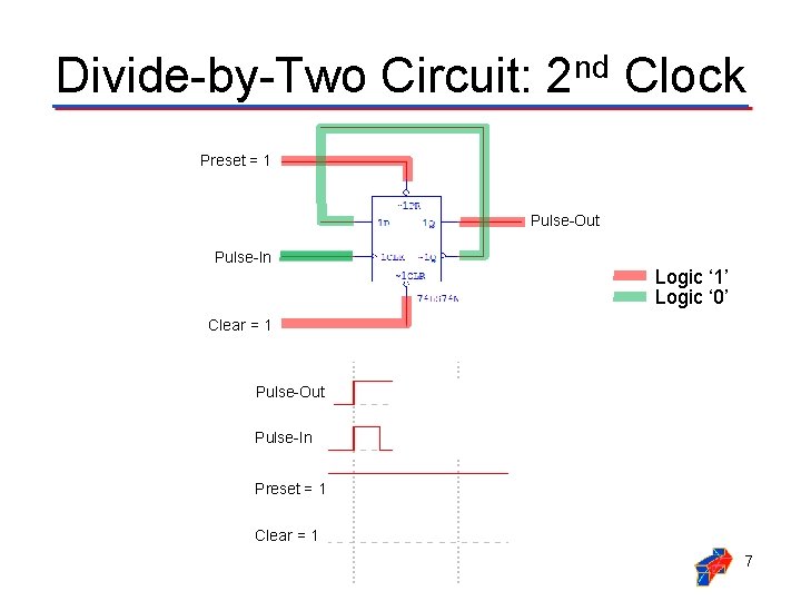
Divide-by-Two Circuit: 2 nd Clock Preset = 1 Pulse-Out Pulse-In Logic ‘ 1’ Logic ‘ 0’ Clear = 1 Pulse-Out Pulse-In Preset = 1 Clear = 1 7

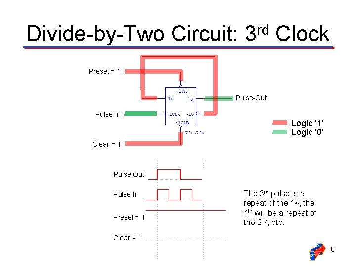
Divide-by-Two Circuit: 3 rd Clock Preset = 1 Pulse-Out Pulse-In Logic ‘ 1’ Logic ‘ 0’ Clear = 1 Pulse-Out Pulse-In Preset = 1 The 3 rd pulse is a repeat of the 1 st, the 4 th will be a repeat of the 2 nd, etc. Clear = 1 8

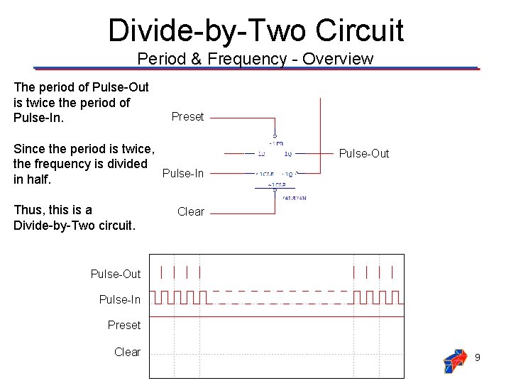
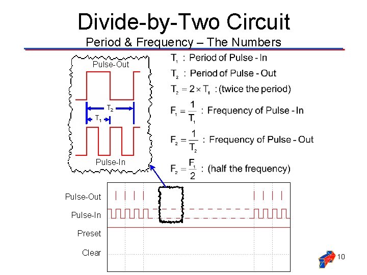
Divide-by-Two Circuit Period & Frequency - Overview The period of Pulse-Out is twice the period of Pulse-In. Preset Since the period is twice, the frequency is divided Pulse-In in half. Thus, this is a Divide-by-Two circuit. Pulse-Out Clear Pulse-Out Pulse-In Preset Clear 9

Divide-by-Two Circuit Period & Frequency – The Numbers Pulse-Out T 2 T 1 Pulse-In Pulse-Out Pulse-In Preset Clear 10

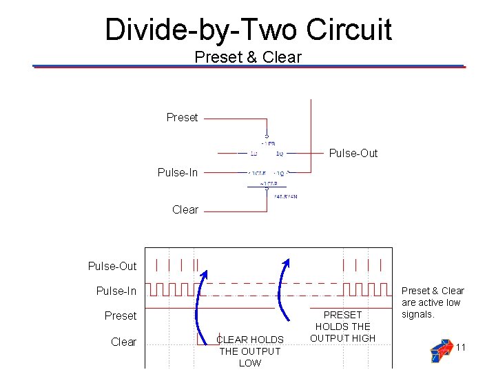
Divide-by-Two Circuit Preset & Clear Preset Pulse-Out Pulse-In Clear Pulse-Out Pulse-In Preset Clear CLEAR HOLDS THE OUTPUT LOW PRESET HOLDS THE OUTPUT HIGH Preset & Clear are active low signals. 11

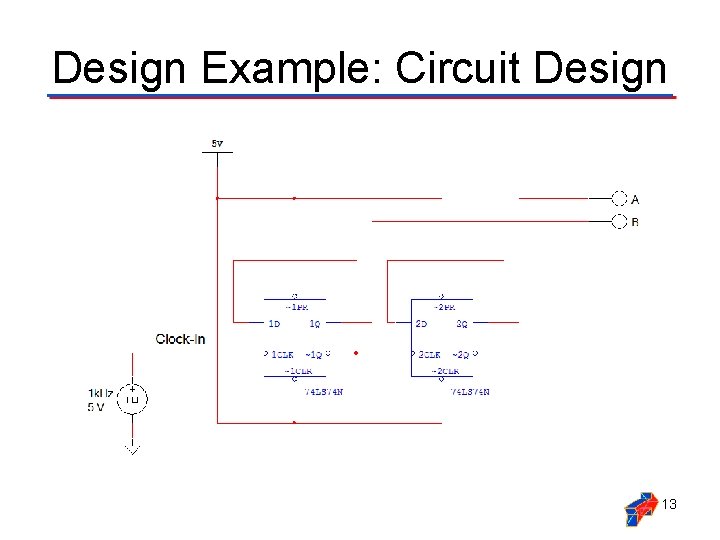
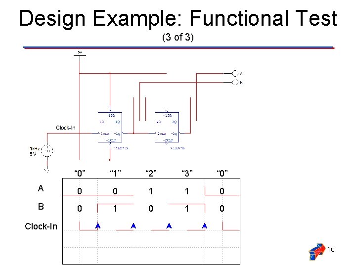
Sequential Logic Design Example The following is a review of the design and operation of a sequential logic circuit using “D” flip-flops. This design is a simple two-bin binary counter that counts from zero (010=002) to three (310=112) and then repeats. 12

Design Example: Circuit Design 13

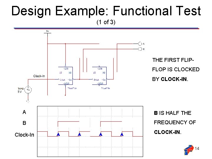
Design Example: Functional Test (1 of 3) THE FIRST FLIPFLOP IS CLOCKED BY CLOCK-IN. A B IS HALF THE B FREQUENCY OF Clock-In CLOCK-IN. 14

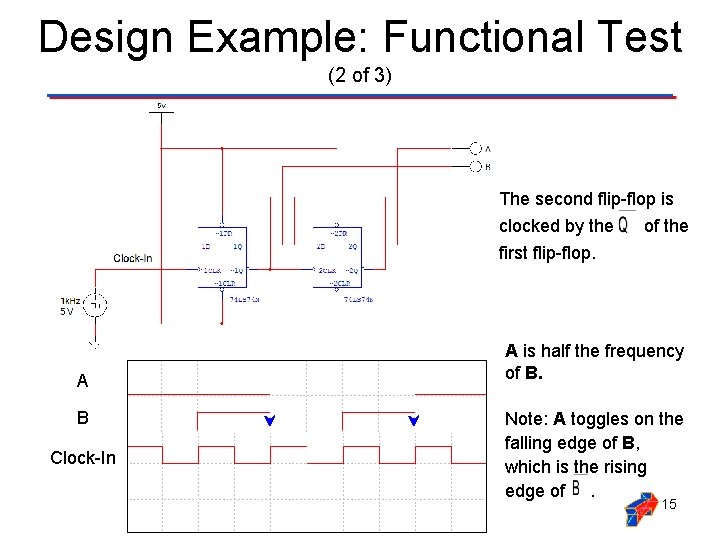
Design Example: Functional Test (2 of 3) The second flip-flop is clocked by the first flip-flop. A B Clock-In of the A is half the frequency of B. Note: A toggles on the falling edge of B, which is the rising edge of. 15

Design Example: Functional Test (3 of 3) “ 0” “ 1” “ 2” “ 3” “ 0” A 0 0 1 1 0 B 0 1 0 Clock-In 16

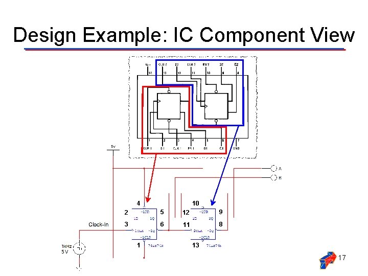
Design Example: IC Component View 10 4 2 5 12 9 3 6 11 8 1 13 17