SEQUENTIAL CIRCUITS USING TTL 74 XX ICS Flip

 Difference between Latch and Flip-flop • • Latches")


 Parallel Data storage: Several bits of data from parallel lines simultaneously")
 Frequency Division: flip-flop is used to divide(reduce) the frequency of a periodic waveform.")
 Counting: Flip-flops are used in digital counters.")


 Pin Diagram Logic Diagram")

 Time Delay Serial in/Serial out shift register is used to provide")

 Serial to parallel data converter Serial data transmission from one digital system to")
 Universal Asynchronous Receiver Transmitter (UART) Computers and microprocessor-based system send and receive data")

 2 -bit asynchronous binary counter")
 3 -bit Asynchronous counter")
4 - bit asynchronous binary counter (IC 7493) Logic Diagram A gated reset inputs,")


- Slides: 32
SEQUENTIAL CIRCUITS USING TTL 74 XX ICS • • Flip Flops (IC 7474, IC 7473), Shift Registers Universal Shift Register(IC 74194) 4 - bit asynchronous binary counter(IC 7493).
Flip Flops (IC 7474, IC 7473) Difference between Latch and Flip-flop • • Latches are controlled by Enable signal and they are Level triggered, either positive or negative level triggered. Flip-flops use Pulse or Clock and it is Edge triggered. In Latches, output state is free to change according to input values, when active level is maintained at Enable input. In Flip-flops, output responds to the changes in input only at positive or negative edge of clock pulse at the clock input.
• FLIP-FLOP: Flip-flops are synchronous bistable devices, also known as bistable multivibrator. Synchronous means output changes state only at a specified point on a triggering input called Clock(CLK), which is designated as a control input. • Types: 1. 2. 3. 4. S-R Flip flop J-K Flip flop D Flip flop T Flip flop
Edge Triggered S-R Flip flop Symbol Truth Table Wave forms
Symbol Edge Triggered J-K Flip flop Wave forms Truth Table
Edge Triggered D Flip flop Truth Table Symbol Wave forms
74 AHC 74 -Dual D Flip-flop Pin Diagram Truth Table
7473 -Dual J-K Flip flop Pin Diagram Truth Table
Flip-Flop Applications 1) Parallel Data storage: Several bits of data from parallel lines simultaneously is stored in a group of flip-flops.
2) Frequency Division: flip-flop is used to divide(reduce) the frequency of a periodic waveform. When a pulse waveform is applied to clock input of a J-K flip-flop that is connected to toggle (J=K=1), Q output is a square wave with one-half the frequency of the clock input. So, a single flip-flop can be applied as a divide-by-2 device.
3) Counting: Flip-flops are used in digital counters.
SHIFT REGISTERS • Shift registers consist of an arrangement of flipflops which are used for storage and transfer of data. • A Register, unlike counter has no specified sequence of states. • A Register is used for storing and shifting data (1 s and 0 s) entered into it from an external source. • DOES TWO FUNCTIONS – DATA STORAGE [DONE BY FLIP-FLOPS] – DATA MOVEMENT[LEFT, RIGHT AND DOWN]
FLIP FLOP AS A STORAGE DEVICE
DATA MOVEMENT IN SHIFT REGISTERS
CLASSIFICATION OF SHIFT REGISTERS • SERIAL IN/SERIAL OUT SHIFT REGISTER • SERIAL IN/ PARALLEL OUT SHIFT REGISTER • PARALLEL IN/ SERIAL OUT SHIFT REGISTER • PARALLEL IN/ PARALLEL OUT SHIFT REGISTER
SERIAL IN / SERIAL OUT SHIFT REGISTER
SERIAL IN /PARALLEL OUTSHIFT REGISTER
PARALLEL IN / SERIAL OUTSHIFT REGISTER
PARALLEL IN/ PARALLEL OUT SHIFT REGISTER
Universal Shift Register(IC 74 HC 194) Pin Diagram Logic Diagram
Truth table
Shift Register-Applications 1) Time Delay Serial in/Serial out shift register is used to provide a time delay from input to output. 8 -bit serial in/serial out shift register is used with a clock frequency of 1 MHz to achieve a time delay (td) of 8µs (8 X 1µs).
Example • Determine the amount of time delay between the serial input and each output in below fig. Show with timing diagram Sol: Clock period is 2µs. Thus, the time delay can be increased or decreased in 2µs. increments from a minimum of 2µs to a maximum of 16µs
2) Serial to parallel data converter Serial data transmission from one digital system to another is commonly used to reduce the number of wires in the transmission line. A computer or microprocessor based system commonly requires incoming data to be in parallel format, thus the requirement for serial to parallel conversion. Serial data format
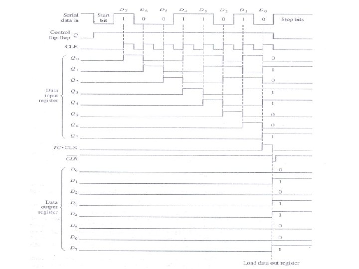
3) Universal Asynchronous Receiver Transmitter (UART) Computers and microprocessor-based system send and receive data in a parallel format. These systems must communicate with external devices that send and/or receive serial data. So, an interfacing device is used to do these conversions, which is called as UART.
Counters • Flip-flops can be connected together to perform counting operations, such a group of flip-flops is called as counter. • Types: 1. Asynchronous counters 2. Synchronous counters. • Asynchronous counter: It is also called as Ripple counter. In this, first flip-flop is clocked by the external clock pulse and then each successive flip-flop is clocked by the output of preceding flip-flop. • Synchronous counter: In this, clock input is connected to all of the flip-flops so that they are clocked simultaneously.
Asynchronous counter 1) 2 -bit asynchronous binary counter
2) 3 -bit Asynchronous counter
3)4 - bit asynchronous binary counter (IC 7493) Logic Diagram A gated reset inputs, Ro(1) and R 0(2). When Ro(1) and R 0(2)=HIGH, counter is reset to 0000 state
Pin Diagram Truth table
IC 74 LS 93 A