Sequential Circuits Prelim on delays and performance Sequential

- Slides: 22

Sequential Circuits • Prelim on delays and performance • Sequential circuits – CLU with feedback loops – Bi-stable (aka S-R flip-flop) – Next time: • Application of flip-flops • Clocked flip-flops, clocked D-flip-flops • Level-triggered, edge-triggered, master-slave flipflops Digital Techniques Fall 2007 André Deutz, Leiden University Slide 1 -1

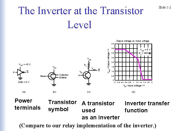
The Inverter at the Transistor Level Slide 1 -2 Output voltage vs. Input voltage VCC = +5 V A RL VCC A Collector Emitter Base Vout Vin A A Vout – Output voltage – V 4. 0 3. 5 VCC = 5 V RL = 400 W 3. 0 2. 5 2. 0 1. 5 1. 0 0. 5 0 GND = 0 V 0 0. 2 0. 4 0. 6 0. 8 1 1. 2 1. 4 1. 6 1. 8 2 Vin– Input voltage– V (a) Power terminals (b) (c) (d) Transistor A transistor Inverter transfer symbol used function as an inverter (Compare to our relay implementation of the inverter. )

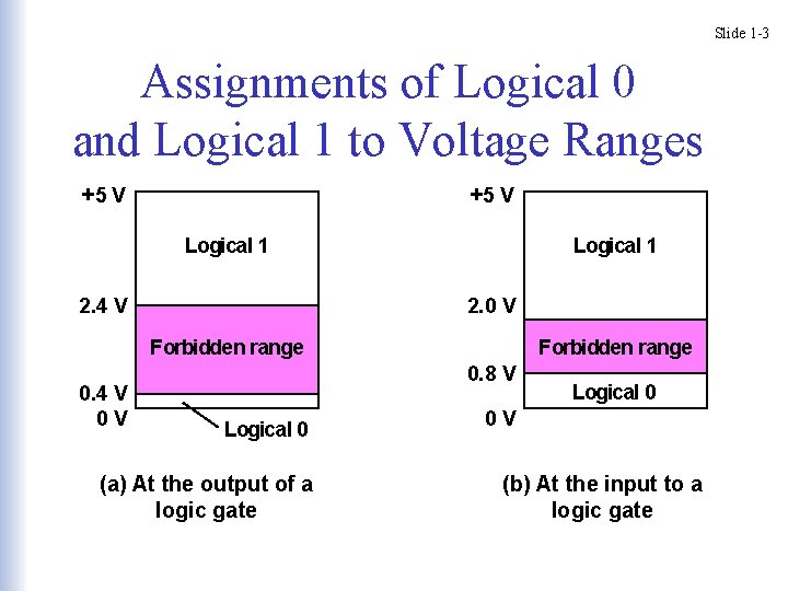
Slide 1 -3 Assignments of Logical 0 and Logical 1 to Voltage Ranges +5 V Logical 1 2. 4 V Logical 1 2. 0 V Forbidden range 0. 4 V 0 V Forbidden range 0. 8 V Logical 0 (a) At the output of a logic gate Logical 0 0 V (b) At the input to a logic gate

Slide 1 -4 Assignments of Logical 0 and Logical 1 to Voltage Ranges +5 V Logical 1 2. 4 V Logical 1 2. 0 V Forbidden range 0. 4 V 0 V Forbidden range 0. 8 V Logical 0 (a) At the output of a logic gate Logical 0 0 V (b) At the input to a logic gate

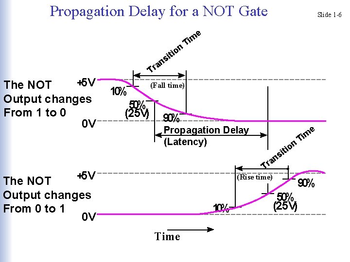
Speed and Performance • The speed of a digital system is governed by – the propagation delay through the logic gates and – the propagation across interconnections. Slide 1 -5

Propagation Delay for a NOT Gate on ti i s Slide 1 -6 e T im n a Tr +5 V The NOT Output changes From 1 to 0 0 V 10% 50% (2. 5 V) (Fall time) 90% Propagation Delay (Latency) e n o iti m Ti ns a r T +5 V The NOT Output changes From 0 to 1 0 V (Rise time) 10% Time 90% 50% (2. 5 V)

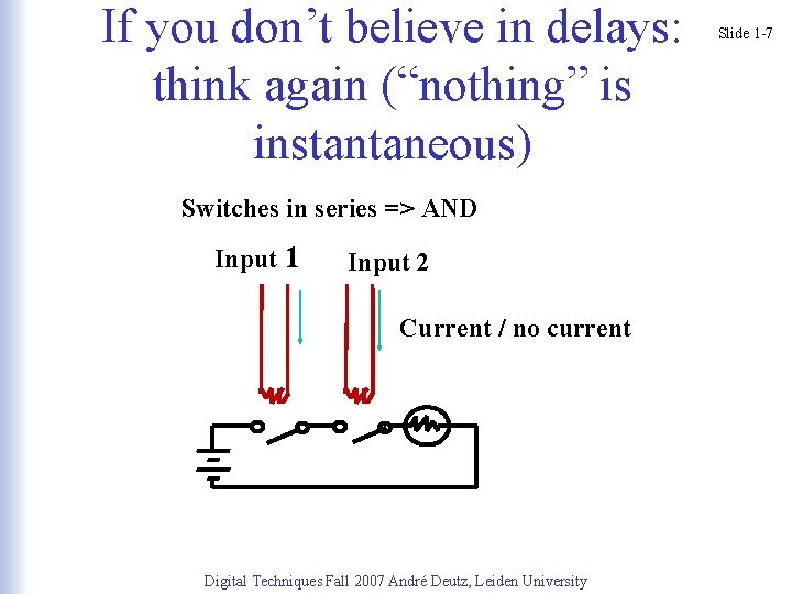
If you don’t believe in delays: think again (“nothing” is instantaneous) Switches in series => AND Input 1 Input 2 Current / no current Digital Techniques Fall 2007 André Deutz, Leiden University Slide 1 -7

Sequential Logic Slide 1 -8 • The combinational logic circuits we have been studying so far have no memory. The outputs always follow the inputs. • There is a need for circuits with a memory, which behave differently depending upon their previous state. • An example is the vending machine, which must remember how many and what kinds of coins have been inserted, and which behave according to not only the current coin inserted, but also upon how many and what kind of coins have been deposited previously. • These are referred to as finite state machines, because they can have at most a finite number of states.

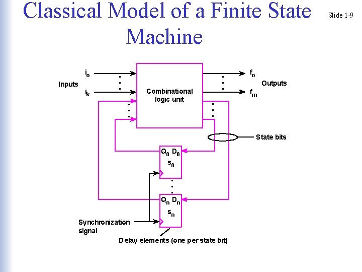
Combinational logic unit . . . ik . . . Inputs fo Outputs fm . . . io . . . Classical Model of a Finite State Machine State bits Q 0 D 0 . . . s 0 Qn D n sn Synchronization signal Delay elements (one per state bit) Slide 1 -9

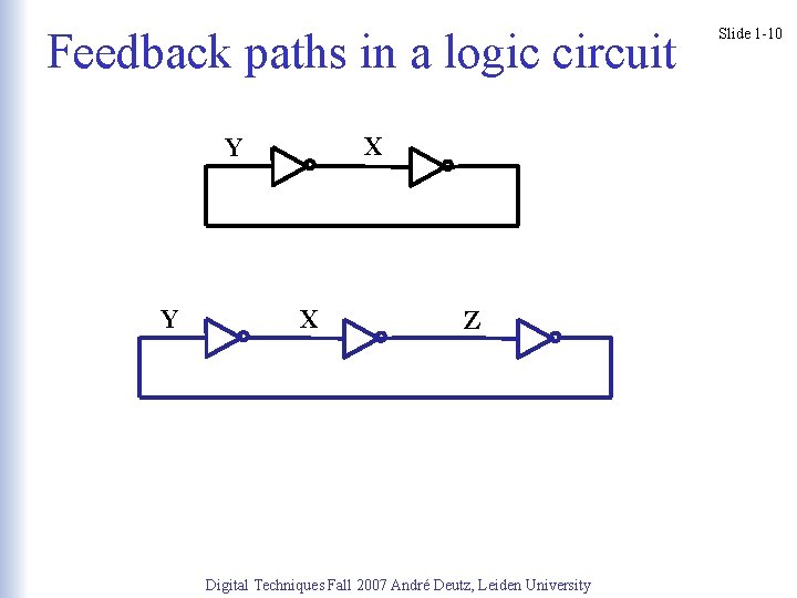
Feedback paths in a logic circuit X Y Y X Z Digital Techniques Fall 2007 André Deutz, Leiden University Slide 1 -10

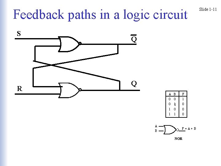
Feedback paths in a logic circuit S R Q Q A B F 0 0 1 1 1 0 0 1 0 1 F = A+ B NOR Slide 1 -11

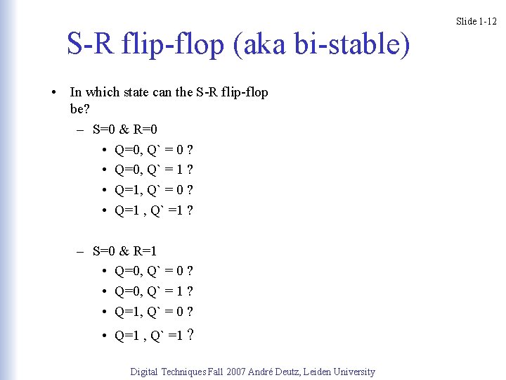
S-R flip-flop (aka bi-stable) • In which state can the S-R flip-flop be? – S=0 & R=0 • Q=0, Q` = 0 ? • Q=0, Q` = 1 ? • Q=1, Q` = 0 ? • Q=1 , Q` =1 ? – S=0 & R=1 • Q=0, Q` = 0 ? • Q=0, Q` = 1 ? • Q=1, Q` = 0 ? • Q=1 , Q` =1 ? Digital Techniques Fall 2007 André Deutz, Leiden University Slide 1 -12

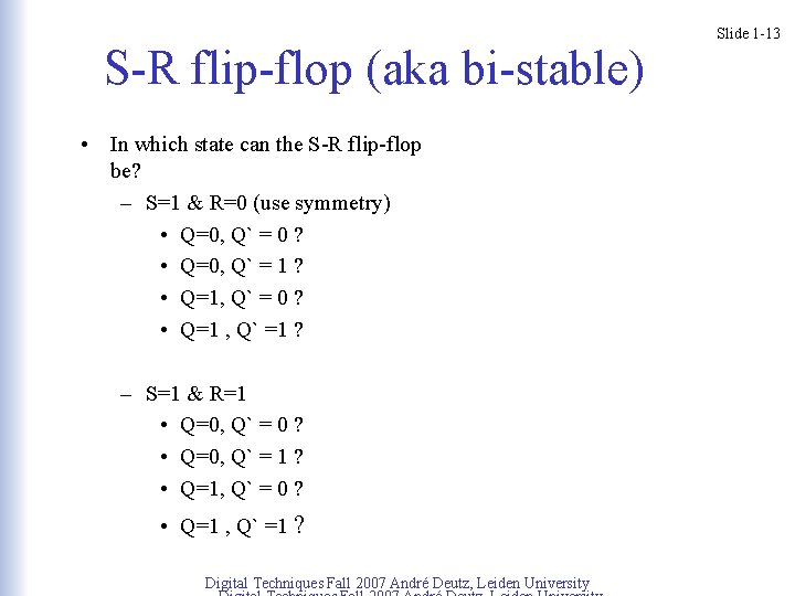
S-R flip-flop (aka bi-stable) • In which state can the S-R flip-flop be? – S=1 & R=0 (use symmetry) • Q=0, Q` = 0 ? • Q=0, Q` = 1 ? • Q=1, Q` = 0 ? • Q=1 , Q` =1 ? – S=1 & R=1 • Q=0, Q` = 0 ? • Q=0, Q` = 1 ? • Q=1, Q` = 0 ? • Q=1 , Q` =1 ? Digital Techniques Fall 2007 André Deutz, Leiden University Slide 1 -13

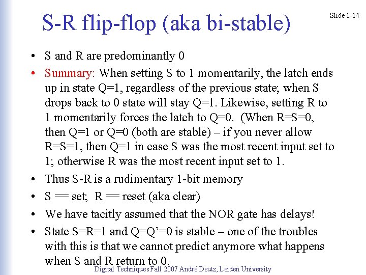
S-R flip-flop (aka bi-stable) Slide 1 -14 • S and R are predominantly 0 • Summary: When setting S to 1 momentarily, the latch ends up in state Q=1, regardless of the previous state; when S drops back to 0 state will stay Q=1. Likewise, setting R to 1 momentarily forces the latch to Q=0. (When R=S=0, then Q=1 or Q=0 (both are stable) – if you never allow R=S=1, then Q=1 in case S was the most recent input set to 1; otherwise R was the most recent input set to 1. • Thus S-R is a rudimentary 1 -bit memory • S == set; R == reset (aka clear) • We have tacitly assumed that the NOR gate has delays! • State S=R=1 and Q=Q’=0 is stable – one of the troubles with this is that we cannot predict anymore what happens when S and R return to 0. Digital Techniques Fall 2007 André Deutz, Leiden University

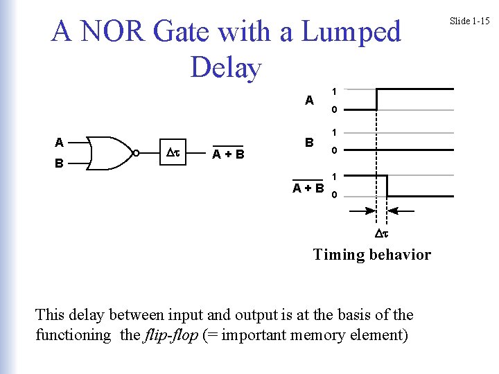
A NOR Gate with a Lumped Delay A A B Dt A+B B A+B 1 0 1 0 Dt Timing behavior This delay between input and output is at the basis of the functioning the flip-flop (= important memory element) Slide 1 -15

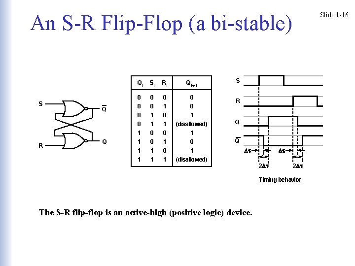
An S-R Flip-Flop (a bi-stable) S R Q Q Qt St Rt Qi+1 0 0 1 1 0 1 0 1 0 0 1 (disallowed) 1 0 1 (disallowed) Slide 1 -16 S R Q Q Dt Dt 2 Dt Timing behavior The S-R flip-flop is an active-high (positive logic) device.

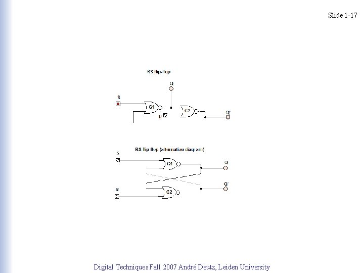
Slide 1 -17 Digital Techniques Fall 2007 André Deutz, Leiden University

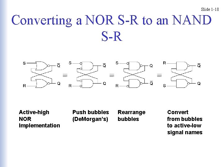
Slide 1 -18 Converting a NOR S-R to an NAND S-R Active-high NOR Implementation Push bubbles (De. Morgan’s) Rearrange bubbles Convert from bubbles to active-low signal names

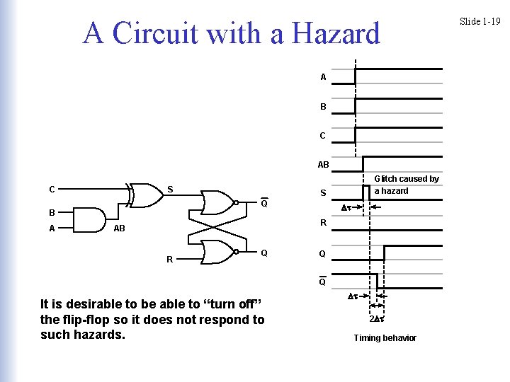
A Circuit with a Hazard A B C AB C S A S Q B Glitch caused by a hazard Dt R AB R Q Q Q It is desirable to be able to “turn off” the flip-flop so it does not respond to such hazards. Dt 2 Dt Timing behavior Slide 1 -19

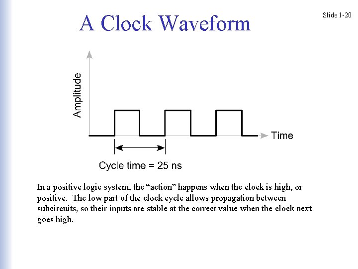
A Clock Waveform In a positive logic system, the “action” happens when the clock is high, or positive. The low part of the clock cycle allows propagation between subcircuits, so their inputs are stable at the correct value when the clock next goes high. Slide 1 -20

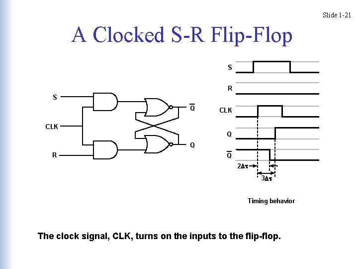
Slide 1 -21 A Clocked S-R Flip-Flop S R S Q CLK Q Q R Q 2 Dt 3 Dt Timing behavior The clock signal, CLK, turns on the inputs to the flip-flop.

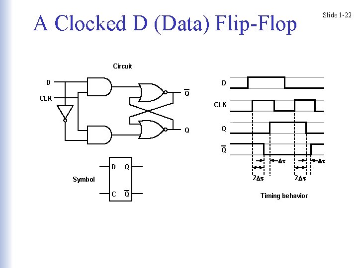
A Clocked D (Data) Flip-Flop Slide 1 -22 Circuit D D Q CLK Q Q Q D Dt Q 2 Dt Symbol C Q Dt 2 Dt Timing behavior