Sequential Circuits Most digital systems like digital watches
- Slides: 35

Sequential Circuits • Most digital systems like digital watches, digital phones, digital computers, digital traffic light controllers and so on require memory elements • Memory elements are digital circuits that can store and retrieve data in the form of 1's and 0's. • The output of the systems with memory depends not only on present inputs but also on what has happened in the past • SR latch is an example of memory circuits that can store one bit of information A. Abhari CPS 213 1

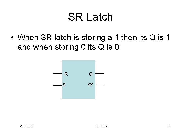
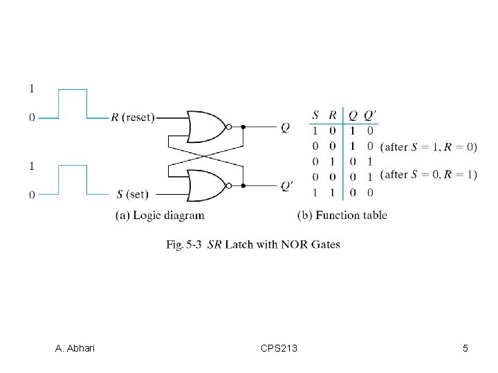
SR Latch • When SR latch is storing a 1 then its Q is 1 and when storing 0 its Q is 0 R S A. Abhari Q Q’ CPS 213 2

SR Latch 1. If SR=10 then Q=1 and the latch is storing a 1, We call this setting the Latch. 2. If SR =10 and we change to SR=00 then the latch will remain set with Q= 1. In other words it "remembers" to stay set 3. If SR=01 then Q=0 and the latch is storing a 0. We call this resetting or Clearing the latch 4. If SR =01 and we change to SR=00 then the latch will remain set with Q= 0. • We call the value of Q at any given time the state of the latch A. Abhari CPS 213 3

SR Latch • The circuit (in next slide) with NOR gates is able to do this because of the feedback from the output back to the input • Note that both Q and Q' are "brought back" and connected to the inputs of the NOR gates • If both S (set) and R (reset) are 1 an undefined state with both output equal to 0 occurs ( it means the SET and RESET commands are issuing at the same time). A. Abhari CPS 213 4

A. Abhari CPS 213 5

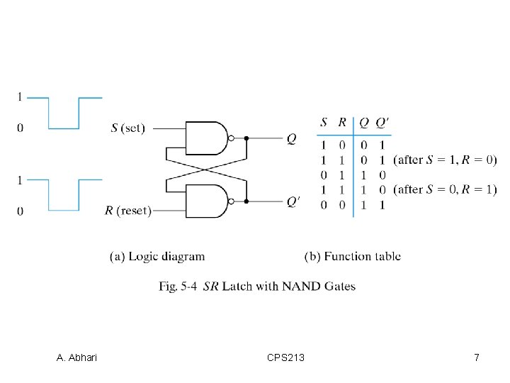
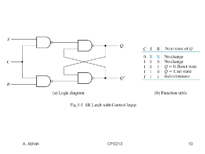
SR Latch • The SR latch with two cross-coupled NAND gate is shown in next slide. • By setting S to 0 the output Q will be 1 that putting the latch in the set state • If S goes to 1 the circuit remains in set state • By setting R to 0 the circuit goes to reset state and stay there even after both input returns to 1 • The undefined state is when both input are 0 • Because NAND latch requires 0 signal to change its state it is also called S’-R’ latch A. Abhari CPS 213 6

A. Abhari CPS 213 7

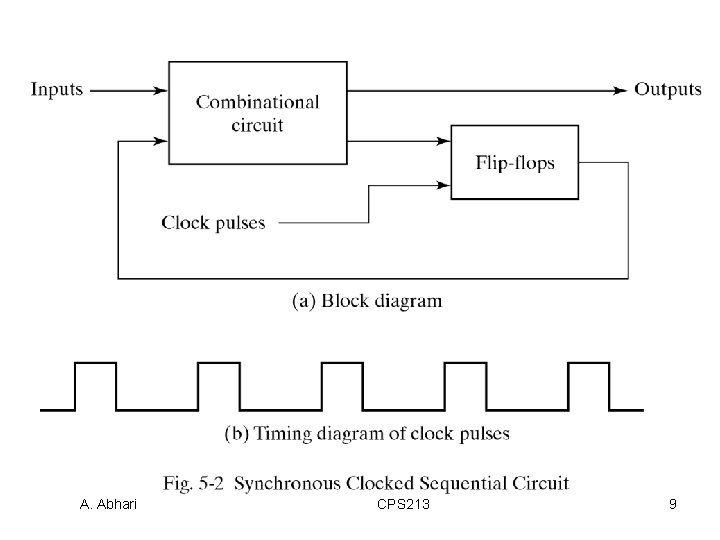
Synchronous vs. Asynchronous • The behavior of a synchronous sequential circuit depends upon the any input signal at any instant of time and order of input change. This synchronization is achieved by clock generators that provides clock pulses (see the next slide). The storage elements used in clocked sequential circuits are called flip-flops. • In asynchronous sequential circuits the storage elements are time delay devices (i. e. , storage is because of their propagation delay). They implemented by feedback that may cause instability in Asynchronous circuits. A. Abhari CPS 213 8

A. Abhari CPS 213 9

A. Abhari CPS 213 10

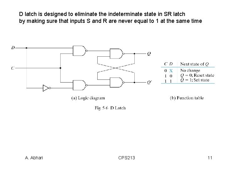
D latch is designed to eliminate the indeterminate state in SR latch by making sure that inputs S and R are never equal to 1 at the same time A. Abhari CPS 213 11

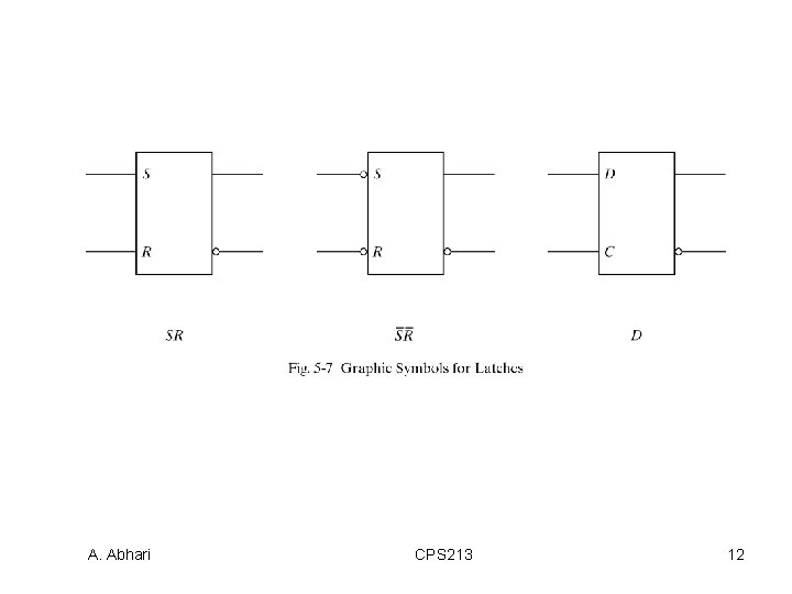
A. Abhari CPS 213 12

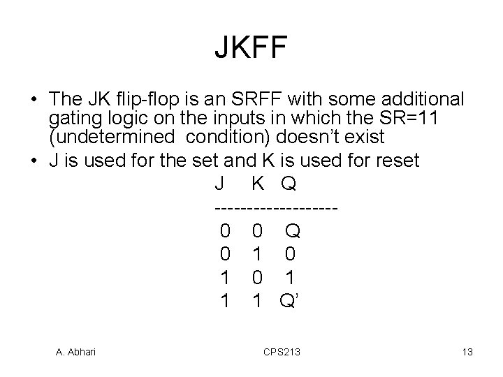
JKFF • The JK flip-flop is an SRFF with some additional gating logic on the inputs in which the SR=11 (undetermined condition) doesn’t exist • J is used for the set and K is used for reset J K Q ---------0 0 Q 0 1 0 1 1 1 Q’ A. Abhari CPS 213 13

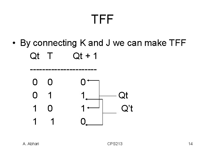
TFF • By connecting K and J we can make TFF Qt T Qt + 1 -----------0 0 1 1 Qt 1 0 1 Q’t 1 1 0 A. Abhari CPS 213 14

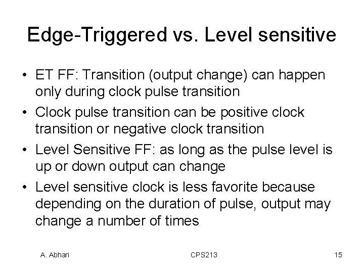
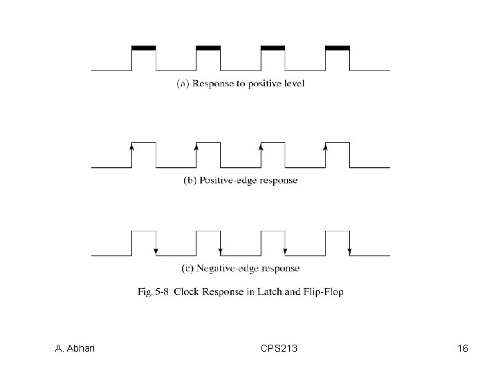
Edge-Triggered vs. Level sensitive • ET FF: Transition (output change) can happen only during clock pulse transition • Clock pulse transition can be positive clock transition or negative clock transition • Level Sensitive FF: as long as the pulse level is up or down output can change • Level sensitive clock is less favorite because depending on the duration of pulse, output may change a number of times A. Abhari CPS 213 15

A. Abhari CPS 213 16

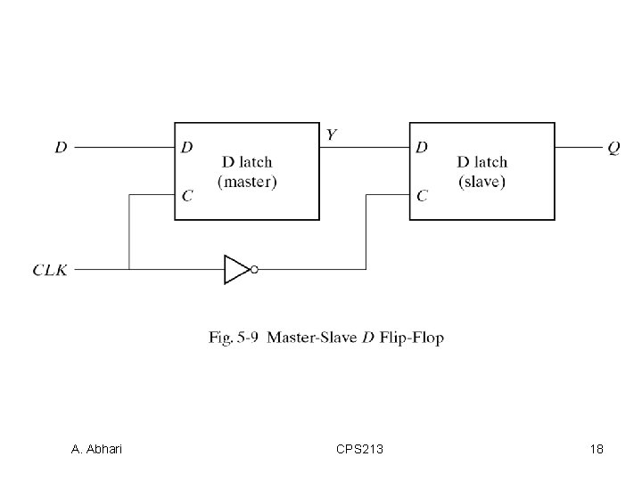
Master-Slave FF (Edge-Trigger FF) • Is a combination of 2 FFS. The first FF is master and responds to positive level of clock • The 2 nd FF is slave and responds to negative level of clock • Therefore, the final output changes only during 1 to 0 transition of clock. It means during the duration of clock pulses changes in input do not have effect on output. A. Abhari CPS 213 17

A. Abhari CPS 213 18

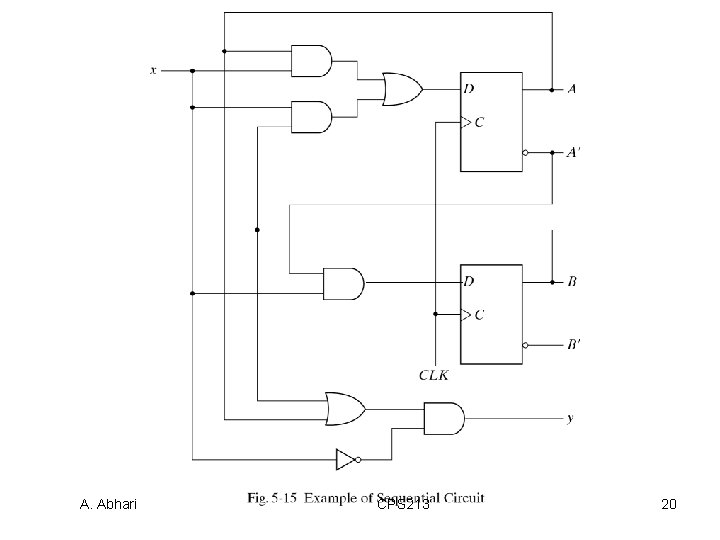
Analysis of Clocked Sequential Circuits • The behaviour of circuit can be described by state equation • For example for the circuit (next slide) the state equations are as the follows: A(t+1) = A(t)x(t) + B(t)x(t) B(t+1)= A’(t). x y(t) = (B(t) + A(t)). x’(t) A. Abhari CPS 213 19

A. Abhari CPS 213 20

State Table • The time sequence of inputs, outputs and flipflop states can be enumerated in a state table or transition table • In the state table the present state that shows the state of flip flops comes first. So n flip flops need n present states. The inputs, next state and output come after. • The combination of present state and inputs makes state table. Output and next state can be derived from the state equations A. Abhari CPS 213 21

State Table There are two types of for state tables: • Mealy Model: In this model sequential circuit or state table the outputs depends on inputs as well as states • Moor Model: Where output depends on state. For example 2 -D version of state table for previous circuit. Where there are only 4 different states and for each state the next states and outputs should be found based on the given inputs. A. Abhari CPS 213 22

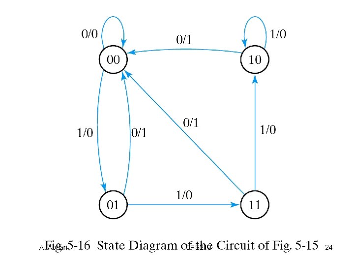
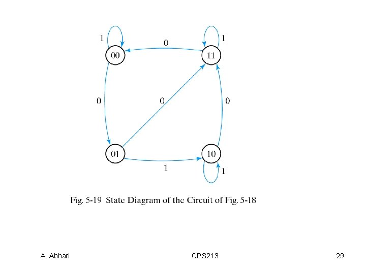
State Diagram • Is the graphically representation of state table. • Each state should be circled so for example if we have n flip flops we have 2 n states or n circles • Each circle should be labeled by a binary number. • By using the state table the arrows can be drawn which show changes from each state to another state. • At the top of each arrow input/output is shown • Also at the top of each arrow only input(s) can be shown. See next slide A. Abhari CPS 213 23

A. Abhari CPS 213 24

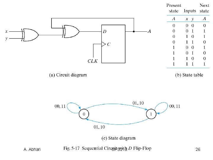
Analysis with D Flip Flop • Next slide is analysis of a D flip flop with one dimensional state table and a state diagram based on Moor Model • Note that two dimensional table state is little bit difficult when there are more inputs and will not discussed here A. Abhari CPS 213 25

A. Abhari CPS 213 26

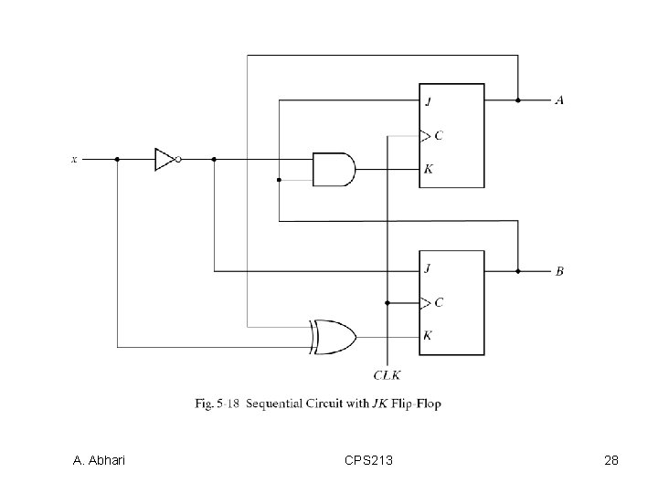
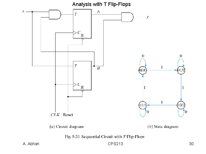
Analysis with JKFF 1. Determine input equations in terms of present state and input varaiables 2. List binary values of each equation 3. Use the corresponding flip-flop characteristics table to determine the next state value in the state table A. Abhari CPS 213 27

A. Abhari CPS 213 28

A. Abhari CPS 213 29

Analysis with T Flip-Flops A. Abhari CPS 213 30

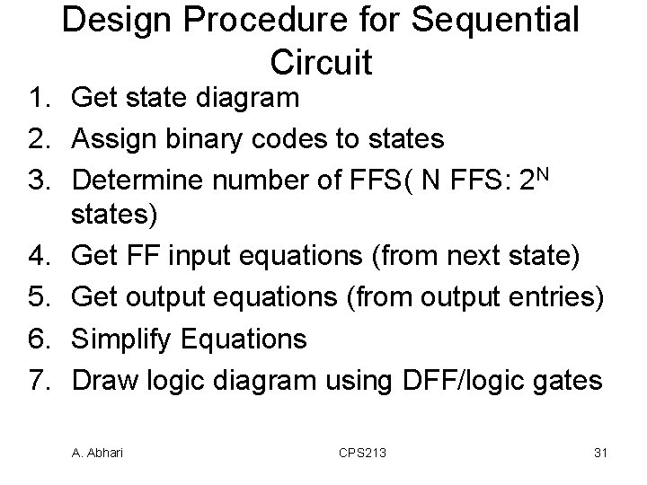
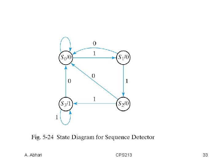
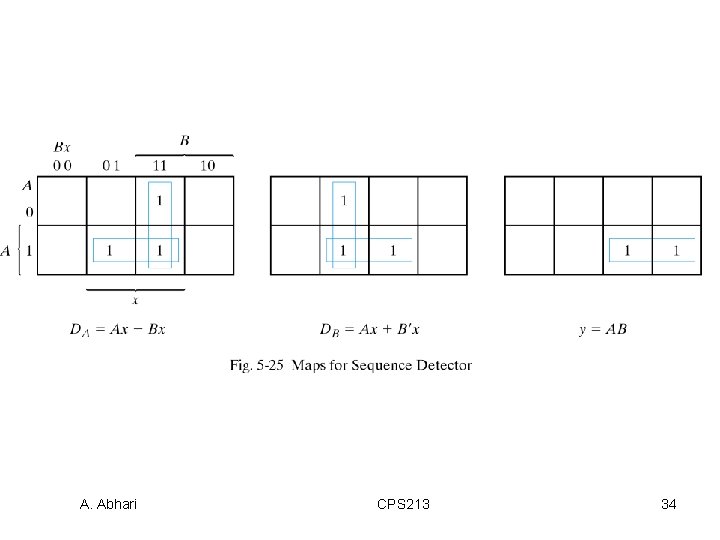
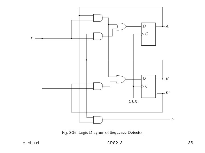
Design Procedure for Sequential Circuit 1. Get state diagram 2. Assign binary codes to states 3. Determine number of FFS( N FFS: 2 N states) 4. Get FF input equations (from next state) 5. Get output equations (from output entries) 6. Simplify Equations 7. Draw logic diagram using DFF/logic gates A. Abhari CPS 213 31

Design Procedure for Sequential Circuit • For example to design a circuit that detects three or more consecutive 1’s in a string of bits coming through an input line we should follow these steps (see next slides) A. Abhari CPS 213 32

A. Abhari CPS 213 33

A. Abhari CPS 213 34

A. Abhari CPS 213 35