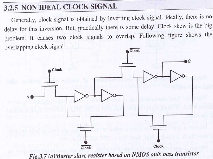
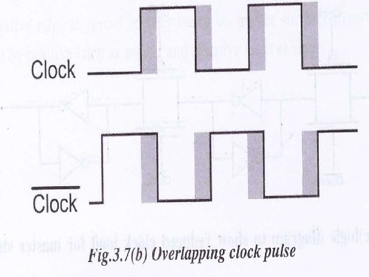
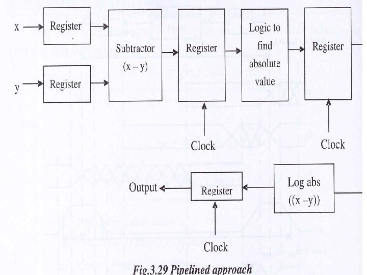
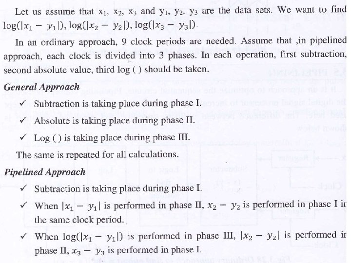
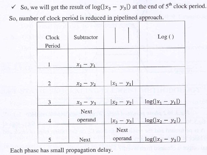
Sequencing Static Circuits latches and flipflops are the
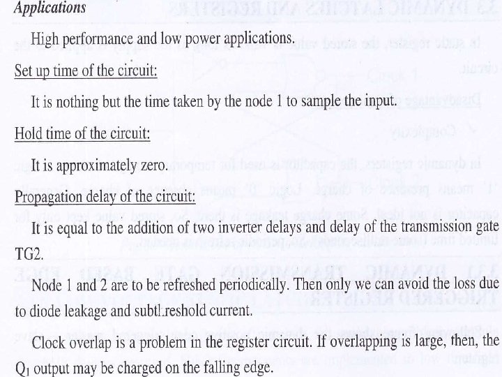


 shows the response of combinational logic to the input")
![] • The contamination delay and propagation delay y be very different because of](https://slidetodoc.com/presentation_image_h/0a3d375a98b882bb62702d5ca63b488a/image-175.jpg "] • The contamination delay and propagation delay y be very different because of")


![]]] • Ideally, the entire clock cycle would be available for computations in the](https://slidetodoc.com/presentation_image_h/0a3d375a98b882bb62702d5ca63b488a/image-178.jpg "]]] • Ideally, the entire clock cycle would be available for computations in the")


![• This is ]]called a race condition, hold-time failure, or min-delay failure. •](https://slidetodoc.com/presentation_image_h/0a3d375a98b882bb62702d5ca63b488a/image-190.jpg "• This is ]]called a race condition, hold-time failure, or min-delay failure. •")


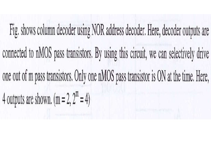
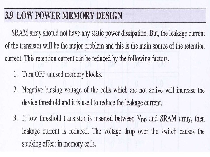
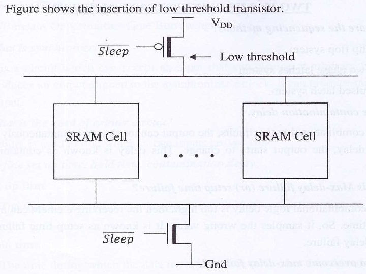
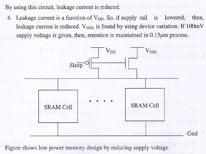
- Slides: 199
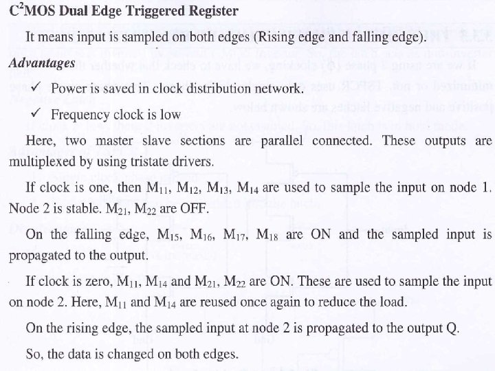
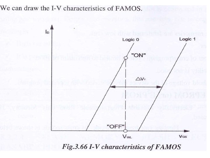
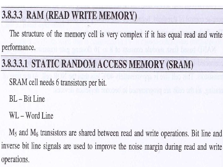
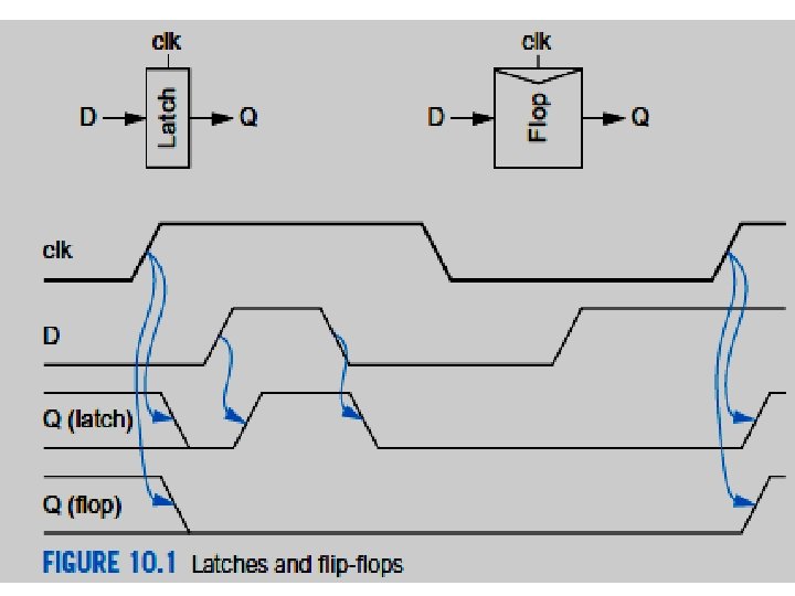
Sequencing Static Circuits • latches and flip-flops are the two most commonly used sequencing elements. • Both have three terminals: data input (D), clock (clk), and data output (Q). • The latch is transparent when the clock is high and opaque when the clock is low; in other words, when the clock is high, D flows through to Q as if the latch were just a buffer, but when the clock is low, the latch holds its present Q output even if D changes.
• The flip-flop is an edge-triggered device that copies D to Q on the rising edge of the clock and ignores D at all other times. These are illustrated in Figure 10. 1. • The unknown state of Q before the first rising clock edge is indicated by the pair of lines at both low and high levels.
• An ideal sequencing methodology would introduce 1. no sequencing overhead, allow sequencing elements back-to-back with no logic in between 2. grant the designer flexibility in balancing the amount of logic in each clock cycle 3. tolerate moderate amounts of clock skew without degrading performance, and consume zero area and power
Sequencing Methods
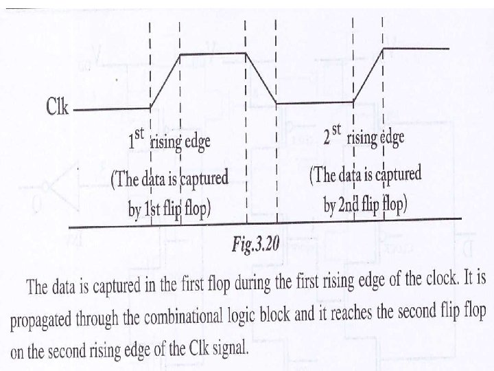
• Figure 10. 2 illustrates three methods of sequencing blocks of combinational logic. • In each case, the clock waveforms, sequencing elements, and combinational logic are shown. • The horizontal axis corresponds to the time at which a token reaches a point in the circuit. • For example, the token is captured in the first flipflop on the first rising edge of the clock.
• It propagates through the combinational logic and reaches the second flip-flop on the second rising edge of the clock. • The dashed vertical lines indicate the boundary between one clock cycle and the next. • The clock period is Tc. • In a 2 -phase system, the phases may be separated by t nonoverlap. • In a pulsed system, the pulse width is tpw.
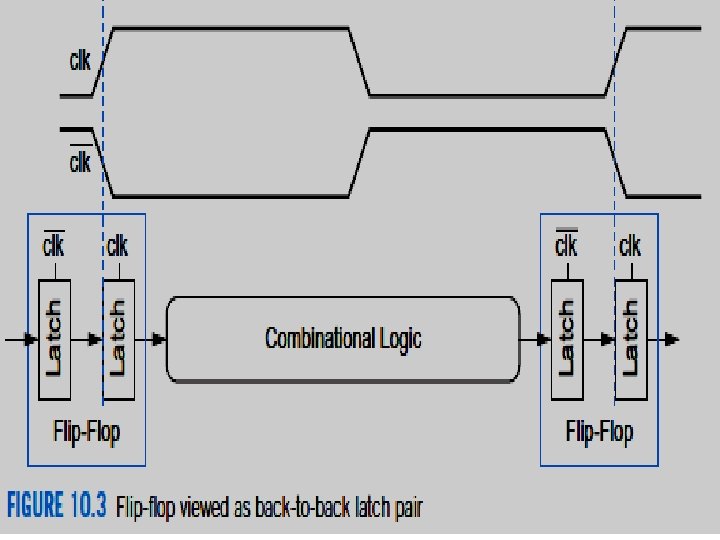
• Flip-flop-based systems use one flip-flop on each cycle boundary. • Tokens advance from one cycle to the next on the rising edge. • If a token arrives too early, it waits at the flip-flop until the next cycle. • Recall that the flip-flop can be viewed as a pair of back-to back latches using clk and its complement
• Flip-flop-based systems use one flip-flop on each cycle boundary. • Tokens advance from one cycle to the next on the rising edge. • If a token arrives too early, it waits at the flip-flop until the next cycle. • Recall that the flip-flop can be viewed as a pair of back-toback latches using clk and its complement, as shown in Figure 10. 3. •
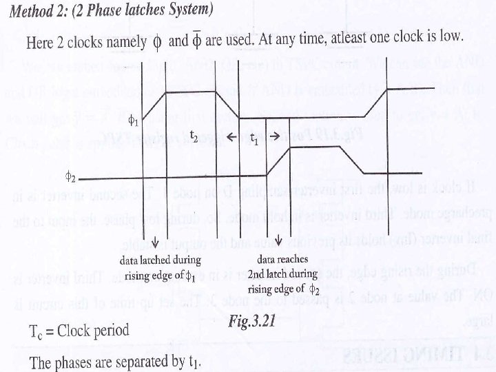
• If we separate the latches, we can divide the full cycle of combinational logic into two phases, sometimes half-cycles. • The two latch clocks are often called and. They may correspond to clk and its complement clk or may be nonoverlapping (tnonoverlap > 0). • A t any given time, at least one clock is low and the corresponding latch is opaque, preventing one token from catching up with another.
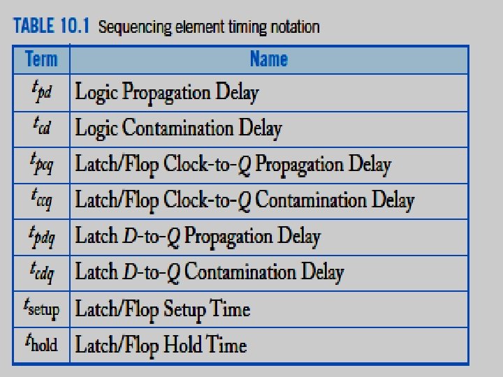
• Table 10. 1 defines the delays and timing constraints of the combinational logic and sequencing elements. • These delays may differ significantly for rising and falling transitions and can be distinguished with an r or f suffix. For brevity, we will use the overall maximum and minimum.
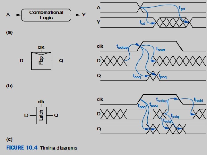
Figure 10. 4 illustrates these delays in a timing diagram • In a timing diagram, the horizontal axis indicates time and the vertical axis indicates logic level. • A single line indicates that a signal is high or low at that time. • A pair of lines indicates that a signal is stable but that we don’t care about its value. • In a timing diagram, the horizontal axis indicates time and the vertical axis indicates logic level. • A single line indicates that a signal is high or low at that time.
• A pair of lines indicates that a signal is stable but that we don’t care about its value. • Criss-crossed lines indicate that the signal might change at that time. • A pair of lines with cross-hatching indicates that the signal may change once or more over an interval of time.
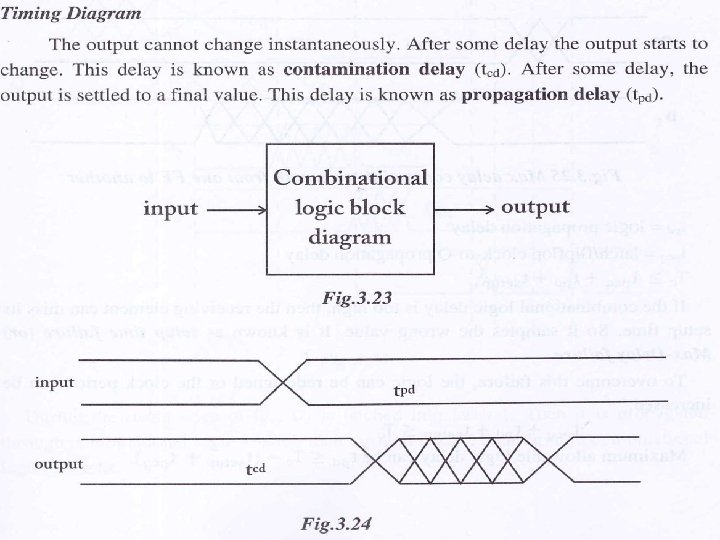
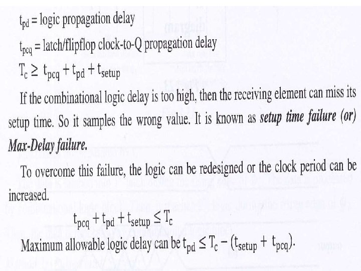
• Figure 10. 4(a) shows the response of combinational logic to the input A changing from one arbitrary value to another • The output Y cannot change instantaneously. • After the contamination delay tcd , Y may begin to change or glitch. • After the propagation delay tpd, Y must have settled to a final value.
] • The contamination delay and propagation delay y be very different because of multiple paths through the combinational logic. • Figure. 4(b) shows the response of a flip-flop. • The data input must be stable for some window around the rising edge of the flop if it is to be reliably sampled • Specifically, the input D must have settled by some setup time tsetup before the rising edge of clk and should not change again until a hold time thold after the clock edge
• The output begins to change after a clock-to-Q contamination delay tccq and completely settles after a clock-to-Q propagation delay tpcq. • Figure 10. 4(c) shows the response of a latch. • Now the input D must set up and hold around the falling edge that defines the end of the sampling period. • The output initially changes tccq after the latch becomes transparent on the rising edge of the clock and settles by tpcq. • While the latch is transparent, the output will continue to track the input after some D-to-Q delay tcdq and tpdq
Max-Delay Constraints
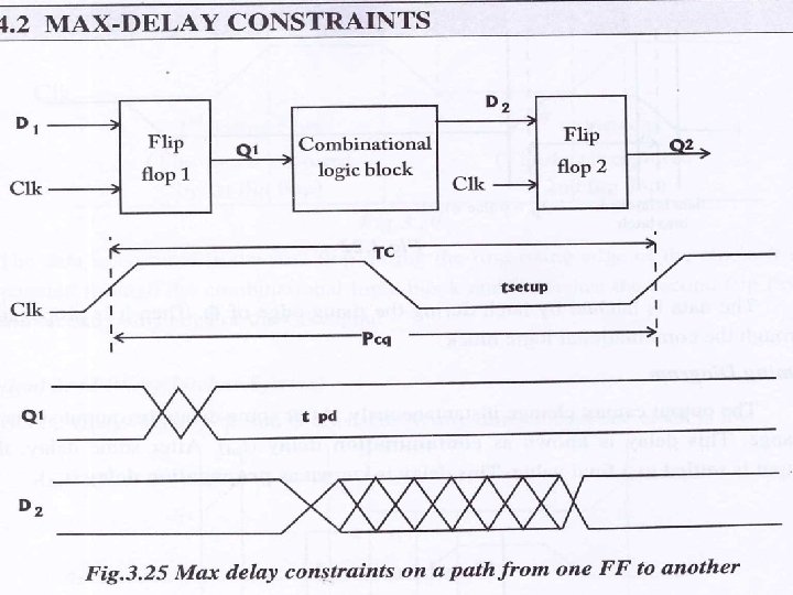
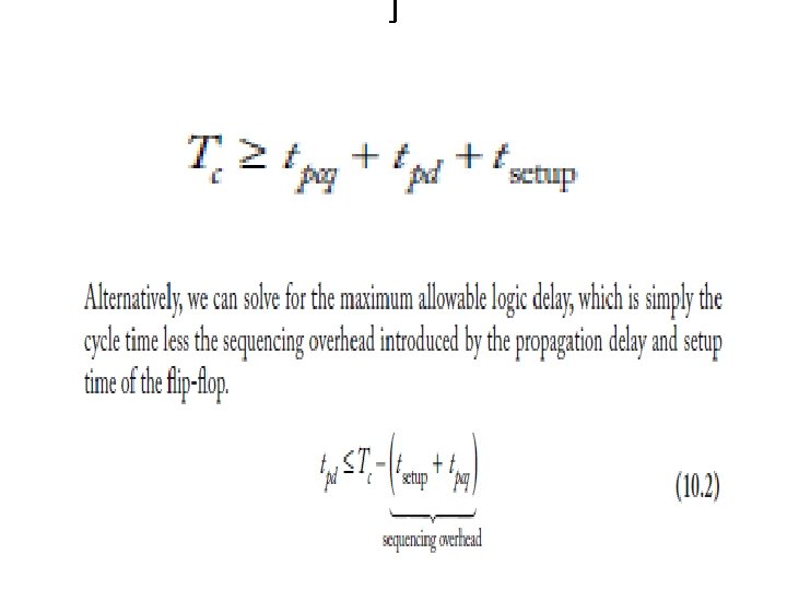
]]] • Ideally, the entire clock cycle would be available for computations in the combinational logic. • seqencing overhead of the latches or flip-flops cuts into this time. • If the combinational logic delay is too great, the receiving element will miss its setup time and sample the wrong value.
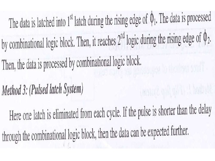
• This is called a setup time failure or max-delay failure. • It can be solved by redesigning the logic to be faster or by increasing the clock period. • This section computes the actual time available for logic and the sequencing overhead of each of our favorite sequencing elements: flip-flops, two-phase latches, and pulsed latches
• Figure 10. 5 shows the max-delay timing constraints on a path from one flip-flop to the next, assuming ideal clocks with no skew. • The path begins with the rising edge of the clock triggering F 1. • The data must propagate to the output of the flipflop Q 1 and through the combinational logic to D 2, setting up at F 2 before the next rising clock edge. • This implies that the clock period must be at least
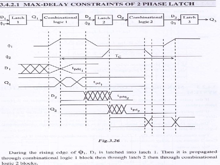
Figure 10. 7 shows the analogous constraint on latches
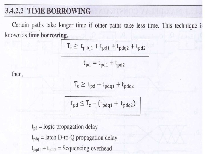
• . Certain paths may take longer if other paths take less time; this technique is called time borrowing Assuming the path takes no more than a cycle, we see the cycle time must be
• Once again, we can solve for the maximum logic delay, which is the sum of the logic delays through each of the two phases. • The sequencing overhead consists of the two latch propagation delays. Notice that the nonoverlap between clocks does not degrade performance in the latch-based system because data continues to propagate through the combinational logic between latches even while both clocks are low.
• Realizing that a flip-flop can be made from two latches whose delays determine the flop propagation delay and setup time, we see EQ (10. 4) is closely analogous to EQ (10. 2).
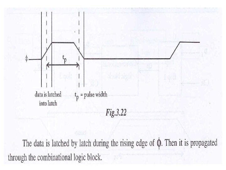
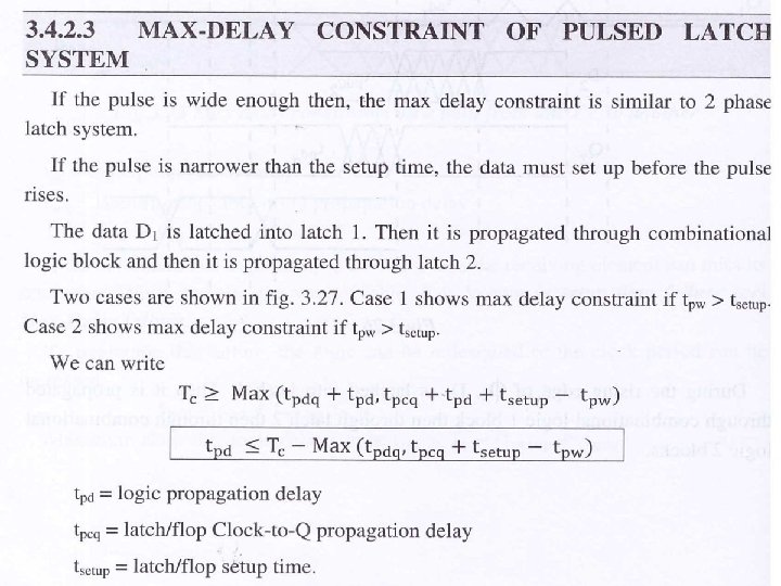
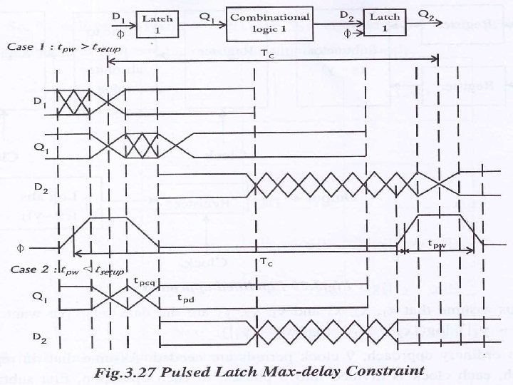
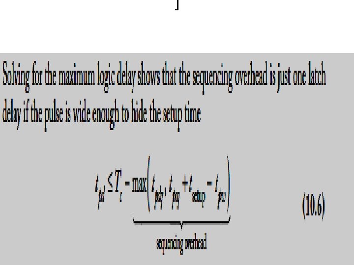
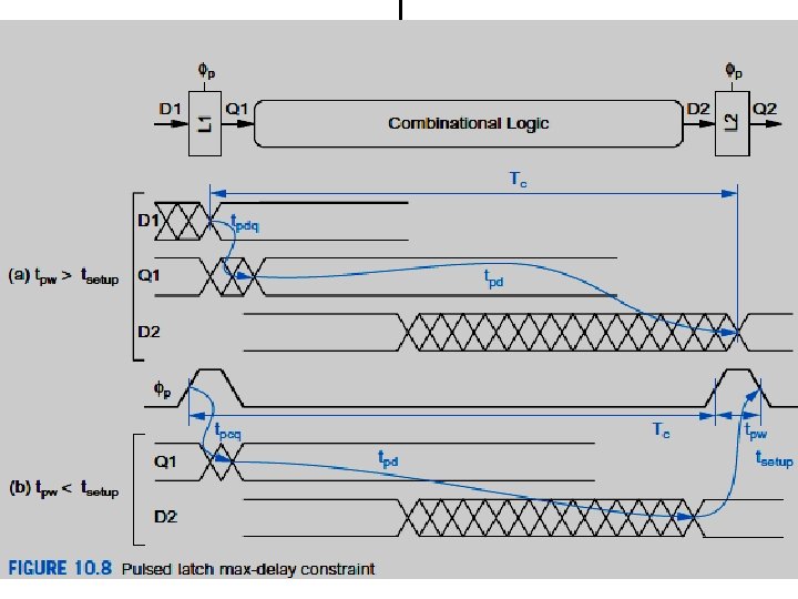
• The max-delay constraint for pulsed latches is similar to that of two-phase latches except that only one latch is in the critical path, as shown in Figure 10. 8(a). • However, if the pulse is narrower than the setup time, the data must set up before the pulse rises, as shown in Figure 10. 8(b). • Combining these two cases gives
Min-Delay Constraints • sequencing elements can be placed back-to-back without intervening combinational logic and still function correctly. • for example, a pipeline can use back-to-back registers to sequence along an instruction opcode without modify • However, if the hold time is large and the contamination delay is small, data can incorrectly propagate through two successive elements on one clock edge, corrupting the state of the system.
• This is ]]called a race condition, hold-time failure, or min-delay failure. • It can only be fixed by redesigning the logic, not by slowing the clock. • Therefore, designers should be very conservative in avoiding such failures because modifying and refabricating a chip is catastrophically expensive and time-consuming.
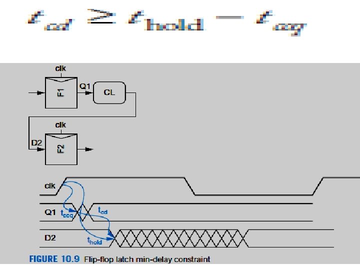
• Figure 10. 9 shows the min-delay timing constraints on a path from one flip-flop to the next assuming ideal clocks with no skew. • The path begins with the rising edge of the clock triggering F 1. • The data may begin to change at Q 1 after a clk-to-Q contamination delay, and at D 2 after another logic contamination delay. • However, it must not reach D 2 until at least the hold time t hold after the clock edge, lest it corrupt the contents of F 2. • Hence, we solve for the minimum logic contamination delay:
• If the contamination delay through the flip-flop exceeds the hold time, you can safely use back-toback flip-flops. • If not, you must explicitly add delay between the flip-flops (e. g. , with a buffer) or use special slow flipflops with greater than normal contamination delay on paths that require back-to-back flops. • Scan chains are a common example of paths with back-to-back flops
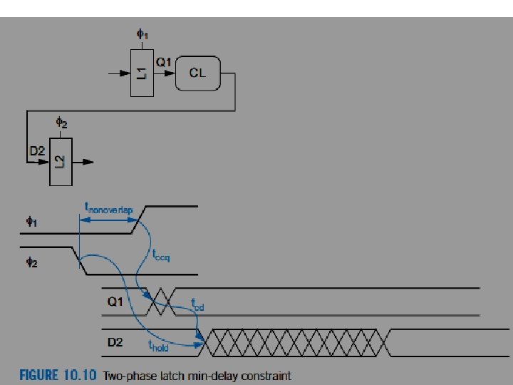
• Figure 10. 10 shows the min-delay timing constraints on a path from one transparent latch to the next. • The path begins with data passing through L 1 on the rising edge of �� 1. • It must not reach L 2 until a hold time after the previous falling edge of �� 2 because L 2 should have become safely opaque before L 1 becomes transparent.
• As the edges are separated by tnonoverlap, the minimum logic contamination delay through each phase of logic is
• This result shows that by making tnonoverlap sufficiently large, hold-time failure can be avoided entirely. • However, generating and distributing nonoverlapping clocks is challenging at high speeds • Therefore, most commercial transparent latchbased systems use the clock and its complement. • In this case, tnonoverlap = 0 and the contamination delay constraint is the same between the latches and flip-flops
Pulsed latch min-delay constraint
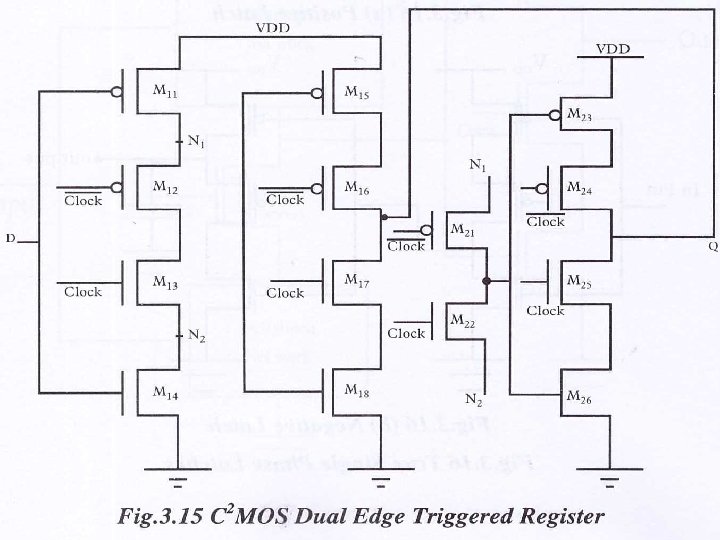
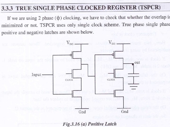
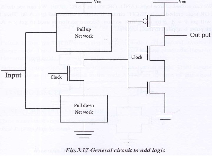
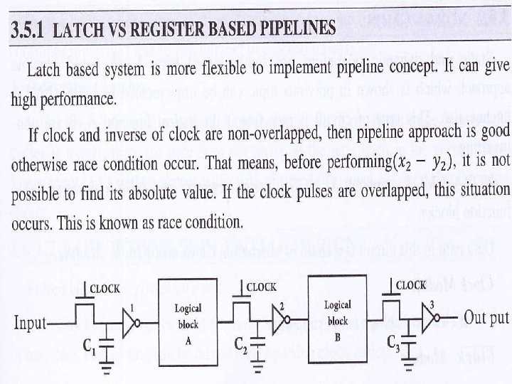
Circuit Design of Latches and Flip. Flops • Conventional CMOS latches are built using pass transistors or tristate buffers to pass the • data while the latch is transparent and feedback to hold the data while the latch is opaque • We begin by exploring circuit designs for basic latches, then build on them to produce • flip-flops and pulsed latches