Sensor Technology group Readout Electronics for Pixel Detectors
- Slides: 12

Sensor Technology group • Read-out Electronics for Pixel Detectors • Establishment of Experimental Research Infrastructure 2001 -03 -14 1

Establishment of Experimental Research Infrastructure • Introduction – Purpose • Establishment of experimental research infrastructure in processing of semiconductor radiation detectors • Educate undergraduate and graduate student in basic semiconductor processing • Support the simulation group with samples-test structures for measuring different kind of semiconductor parameters – Requirement • The equipment in the clean room must be easy to use and be as flexible as possible • The equipment must handle small pieces, to wafers with a diameter of 100 mm • The most common processing steps must be represented Departement of Information Technology and Media Sensor Technology 2

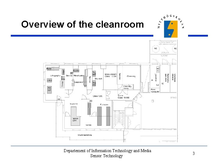
Overview of the cleanroom Departement of Information Technology and Media Sensor Technology 3

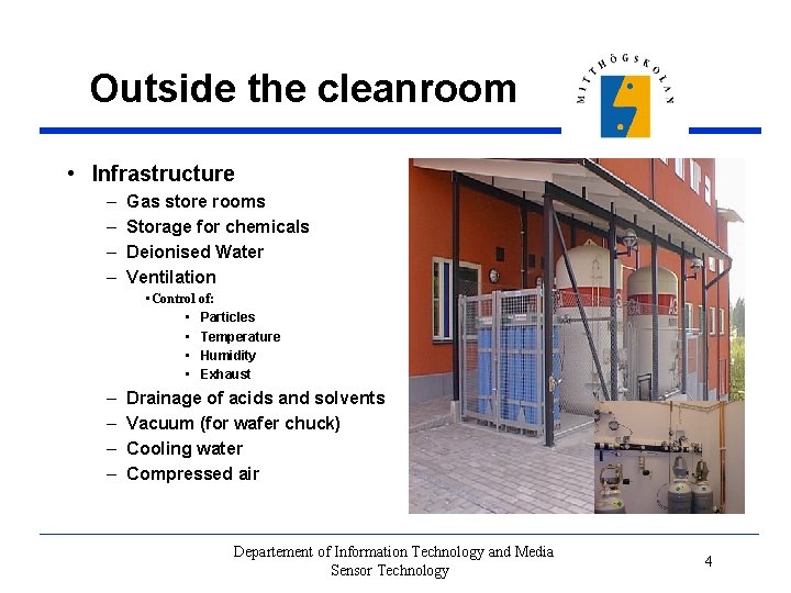
Outside the cleanroom • Infrastructure – – Gas store rooms Storage for chemicals Deionised Water Ventilation • Control of: • Particles • Temperature • Humidity • Exhaust – – Drainage of acids and solvents Vacuum (for wafer chuck) Cooling water Compressed air Departement of Information Technology and Media Sensor Technology 4

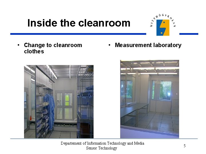
Inside the cleanroom • Change to cleanroom clothes • Measurement laboratory Departement of Information Technology and Media Sensor Technology 5

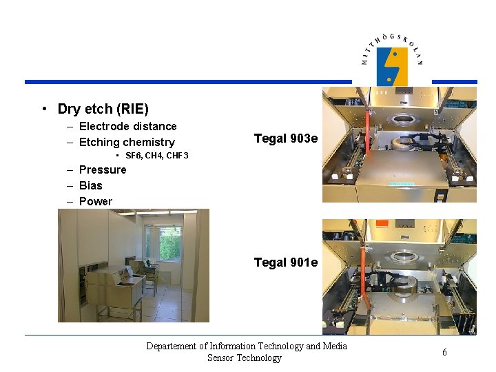
• Dry etch (RIE) – Electrode distance – Etching chemistry Tegal 903 e • SF 6, CH 4, CHF 3 – Pressure – Bias – Power Tegal 901 e Departement of Information Technology and Media Sensor Technology 6

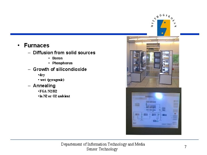
• Furnaces – Diffusion from solid sources • Boron • Phosphorus – Growth of silicondioxide • dry • wet (pyrogenic) – Annealing • FGA N 2/H 2 • in N 2 or O 2 ambient Departement of Information Technology and Media Sensor Technology 7

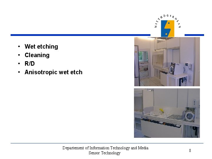
• • Wet etching Cleaning R/D Anisotropic wet etch Departement of Information Technology and Media Sensor Technology 8

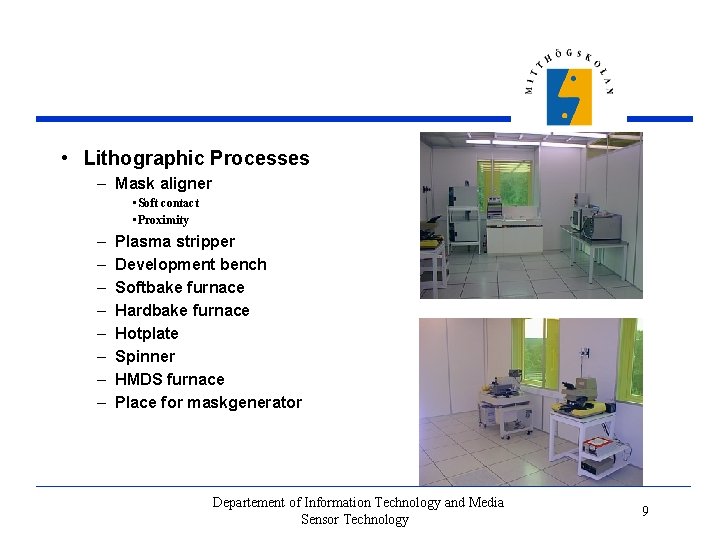
• Lithographic Processes – Mask aligner • Soft contact • Proximity – – – – Plasma stripper Development bench Softbake furnace Hardbake furnace Hotplate Spinner HMDS furnace Place for maskgenerator Departement of Information Technology and Media Sensor Technology 9

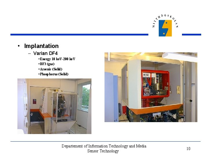
• Implantation – Varian DF 4 • Energy 10 ke. V-200 ke. V • BF 3 (gas) • Arsenic (Solid) • Phosphorus (Solid) Departement of Information Technology and Media Sensor Technology 10

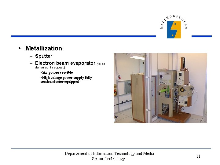
• Metallization – Sputter – Electron beam evaporator (to be delivered in august) • Six pocket crucible • High voltage power supply fully semiconductor equipped Departement of Information Technology and Media Sensor Technology 11

• Education – Course in “Vacuum Technology for Semiconductor Processing” (Given by Doc. Lars Westerberg, chairmen in Swedish Vacuum Society) • Lectures • Laboratory exercise • Study visit at The Svedberg laboratory in Uppsala – Test structures in Si. C – Laboratory exercise for the students in the processing of pn-diodes • Recruit of PHD students to work in semiconductor processing • Planned Project – Pixel detector in silicon – Integrated DE-E detector in silicon – UV-detector in silicon with two layers antireflective coating – Quadrant detector in silicon Departement of Information Technology and Media Sensor Technology 12